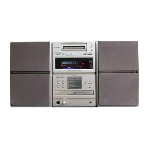
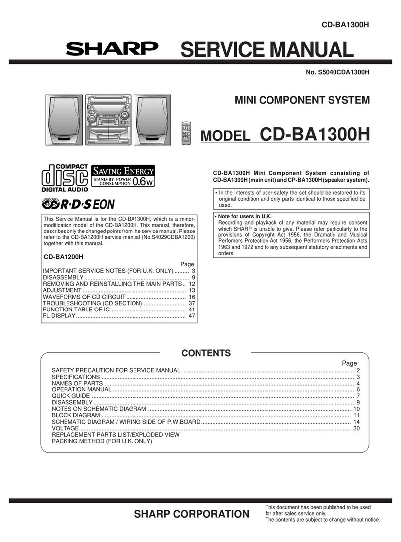
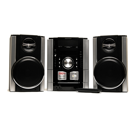
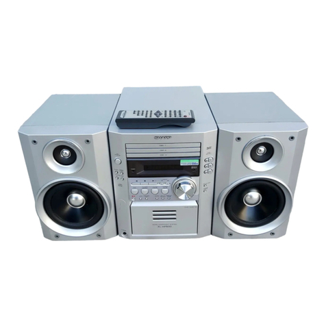
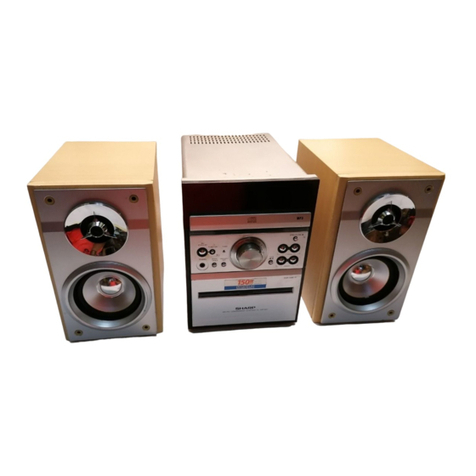
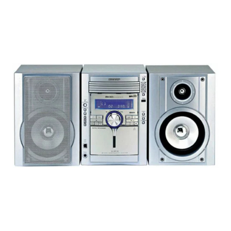
Sharp XL-DV5 User manual

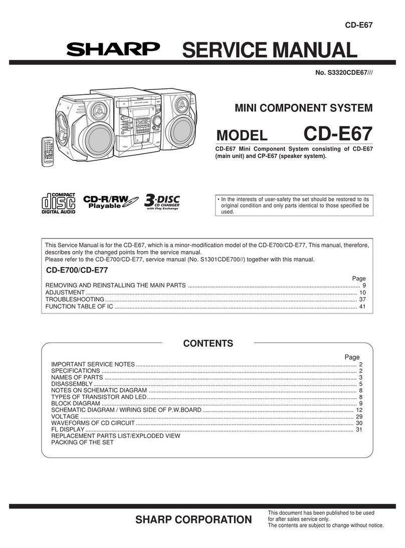
SERVICE MANUAL
XL-DV5/DV50
No. S6433XLDV50U/
DVD MICRO SYSTEM
XL-DV5
MODEL
SHARP CORPORATION
CONTENTS
This document has been published to be used
for after sales service only.
The contents are subject to change without notice.
CHAPTER 1. GENERAL DESCRIPTION
[1] IMPORTANT SERVICE NOTES (FOR
U.S.A. ONLY).................................................1-1
[2] SPECIFICATIONS .........................................1-2
[3] NAMES OF PARTS........................................1-3
CHAPTER 2. ADJUSTMENTS
[1] ADJUSTMENT...............................................2-1
[2] TEST MODE..................................................2-2
CHAPTER 3. MECHANICAL DESCRIPTION
[1] REMOVING AND REINSTALLING THE
MAIN PARTS .................................................3-1
[2] DISASSEMBLY..............................................3-2
CHAPTER 4. DIAGRAMS
[1] BLOCK DIAGRAM.........................................4-1
CHAPTER 5. CIRCUIT DESCRIPTION
[1] VOLTAGE.......................................................5-1
CHAPTER 6. CIRCUIT SCHEMATICS AND PARTS
LAYOUT
[1] NOTES ON SCHEMATIC DIAGRAM............6-1
[2] TYPES OF TRANSISTOR AND LED............6-1
[3] WIRING SIDE OF PWB/SCHEMATIC DIA-
GRAM............................................................6-2
CHAPTER 7. FLOWCHART
[1] TROUBLESHOOTING ..................................7-1
CHAPTER 8. OTHERS
[1] FUNCTION TABLE OF IC .............................8-1
[2] FL DISPLAY ..................................................8-4
Parts Guide
XL-DV5 DVD Micro System consisting of XL-DV5 (main
unit), CP-DV5F (front speakers) and CP-DV5SW(subwoof-
er).
•
In the interests of user-safety the set should be restored to its origi-
nal condition and only parts identical to those specified be used.
XL-DV50
MODEL
XL-DV50 DVD Micro System consisting of XL-DV50 (main
unit), CP-DV50F (front speakers) and CP-DV50SW(sub-
woofer).
Illustration XL-DV5

XL-DV5/DV50
1 – 1
AudioXL-DV5/DV50Service ManualXLDV50/5MarketE
CHAPTER 1. GENERAL DESCRIPTION
[1] IMPORTANT SERVICE NOTES (FOR
U.S.A. ONLY)
BEFORE RETURNING THE AUDIO PRODUCT
(Fire & Shock Hazard)
Before returning the audio product to the user, perform the following
safety checks.
1. Inspect all lead dress to make certain that leads are not pinched or
that hardware is not lodged between the chassis and other metal
parts in the audio product.
2. Inspect all protective devices such as insulating materials, cabinet,
terminal board, adjustment and compartment covers or shields,
mechanical insulators etc.
3. To be sure that no shock hazard exists, check for leakage current in
the following manner.
* Plug the AC line cord directly into a 120 volt AC outlet.
* Using two clip leads, connect a 1.5k ohm, 10 watt resistor paral-
leled by a 0.15µF capacitor in series with all exposed metal cabinet
parts and a known earth ground, such as conduit or electrical
ground connected to earth ground.
* Use a VTVM or VOM with 1000 ohm per volt, or higher, sensitivity
to measure the AC voltage drop across the resistor (See diagram).
* Connect the resistor connection to all exposed metal parts having a
return path to the chassis (antenna, metal cabinet, screw heads,
knobs and control shafts, escutcheon, etc.) and measure the AC
voltage drop across the resistor.
All check must be repeated with the AC line cord plug connection
reversed.
Any reading of 0.3 volt RMS (this corresponds to 0.2 milliamp. AC.) or
more is excessive and indicates a potential shock hazard which must
be corrected before returning the audio product to the owner.
FOR A COMPLETE DESCRIPTION OF THE OPERATION OF THIS UNIT, PLEASE REFER
TO THE OPERATION MANUAL.
TO EXPOSED
METAL PARTS
CONNECT TO
KNOWN EARTH
GROUND
TEST PROBE
0.15 µ F
1.5k ohms
10W
VTVM
AC SCALE

XL-DV5/DV50
1 – 2
[2] SPECIFICATIONS
Specifications for this model are subject to change without prior notice.
■General
■
Power AC 120 V, 60 Hz
Power 108 W
Width: 6-5/16" (160 mm)
Height: 9-7/16" (240mm)
Depth: 11-13/16" (300 mm)
Weight 13.0 lbs. (5.9 kg)
Output power Front speakers: 30 watts minimum RMS
per channel into 6 ohms from 100 Hz to 20
kHz, 10% total harmonic distortion
Subwoofer: 40 watts minimum RMS into 6
ohms from 70 Hz to 130 Hz, 10% total har-
monic distortion
output Front speakers and subwoofer: 6 ohms
Headphones: 16 - 50 ohms
(recommended: 32 ohms)
Optical digital output: Square type 1
Audio input
terminals
Video/Auxiliary (audio signal): 500 mV/47 k
ohms
Video Video output: RCA type 1
S-video output: S-terminal 1
Component video output: RCA type 1
■DVD player
■
■Front
■
Type 5-disc multi-play compact disc player
readout NTSC color
DVD (region number 1, ALL), video CD, au-
dio CD, CD-R, CD-RW
Video signal Horizontal resolution: 500 lines
S/N ratio: 75 dB
Frequency
characte ris-
tics
Linear PCM DVD: 30 Hz to
20 kHz (sampling rate: 48
kHz)
30 Hz to 20 kHz (sampling
rate: 96 kHz)
CD: 30 Hz to 20 kHz
S/N ratio CD: 95 dB (1 kHz)
Dynamic
range
Linear PCM DVD: 92 dB
CD: 92 dB
Total har-
monic distor-
tion r atio
0.14 %
Frequency range FM: 87.5 - 108 MHz
AM: 530 - 1,720 kHz
Type 2-way type speaker system (Magnetic
shield)
1.5" (4 cm) tweeter
4" (10 cm) woofer
Maximum input 60 W
Rated 30 W
Impedance 6 ohms
Dimensions Width: 6-1/2" (165 mm)
Height: 9-7/16" (240 mm)
Depth: 10-7/16" (265mm)
Weight 5.5 lbs. (2.5 kg)/each
Type 6" (15 cm) subwoofer system (Magnetic
shield)
Maximum input 80 W
Rated 40 W
Impedance 6 ohms
Width: 6-5/16" (160 mm)
Height: 9-7/16" (240 mm)
Depth: 10-5/8" (270 mm)
6.4 lbs. (2.9 kg)/each
source
consumption
Dimensions
terminals
output
terminals
Signal
Supported
disc
types
Audio signal
Weight
Dimensions
inputpower
power
Subwoofer
inputpower
power
speaker
Tuner
Audio
Amplifier

XL-DV5/DV50
1 – 3
[3] NAMES OF PARTS
■Front
1. Equalizer Mode Select Button
2. Extra Bass/Demo Mode
3. Timer Indicator
4. Power On/Stand-by Button
5. DVD/CD
6. Tuner (Band)
7. Video/Auxiliary
8. Compartment
9. Jack
10. Remote Sensor
11. Stop or Down
12. Play or Tuning Up
13. Chapter (Track) Skip Down or Fast Reverse,
Tuner Preset Button
14. Chapter (Track) Skip Up or Fast Forward,
Tuner Preset Up Button
15. Memory
16. Compartment Open/Close Button
17. Number Select Buttons
18. Volume Control
■Display
1.Number
2.Play
3.
4.Repeat Play
5.Disc Type
6. Extra
7.Sleep
8.Timer Play
9.Sound Mode
10.Memory
11.
12.Surround Mode
13.FM Stereo Mode
14. FM Stereo Receiving
10
18
11
12
13
14
15
16
17
321 4 5678
9
13 1410 11 12
4
8
9
1
2
3
5
6
7
panel
Button
Button
Button
Button
Button
Button
Button
Disc
Headphone
Tuning
Down
/Set
Disc
Disc
Disc Indicators
Indicators
Indicator
Indicator
Pause
Indicators
Indicators
Indicator
Indicator
Indicator
Indicator
Indicator
Indicator
Indicator
Indicator
Bass
Angle
1
3
5
6
4
7
8
9
3
3
4
2
1
2
1
2
■Rear panel
1.AC Power Input Jack
2. Speaker Terminals
3.Video Output Jacks
4.
5.FM/AM Loop Antenna Jack
6.Video/Auxiliary (Audio Signal) Input Jacks
7.Video Output Jack
8.S-video Output Jack
9.Optical Digital Audio Output Jack
■Front
1. Tweeter
2. Woofer
3. Bass Duct
4. Speaker Wire
■
1.Sub Pipe
2.
3. Speaker Wire
Component
Cooling Fan
speaker
Reflex
Subwoofer
Duct
Subwoofer

XL-DV5/DV50
1 – 4
■
1.Control Transmitter
2.DVD Setup
3.Power On/Stand-by Button
4.Number
5.Chapter (Track) Skip Down or Fast Reverse,
Tuner Preset Down, Time Down
6.Cursor Buttons
7.Zoom or Audio Select
8.Repeat Play Button
9.Frame Advance or Pause
10.A - B Repeat Button
11.Memory/Set Button
12.Top Menu or Return Button
13.Subtitle or Surround Mode Select
14.Shift
15. Extra or Digital Picture Select
16.DVD/CD
17.Equalizer Mode Select or Gamma Button
18.Tuner (Band)
19.Menu or On Display Select
20.Disc Number Select Buttons
21.or Video Mode Select
22.Chapter (Track) Skip Up or Fast
Tuner Preset Up, Time Up
23.Enter Button
24.Angle Select Button
25.Play Button
26.Stop Button
27.Random Button
28.Clear Button
29.Timer/Sleep Button
30.Clock Button
31.Video/Auxiliary Button
32.Volumeor LevelUpandDownButtons
1
2
26
25
27
28
29
30
32
31
24
23
22
21
20
19
5
6
7
8
9
10
11
12
13
14
15
16
17
18
3
4
Direct
Button
Button
Button
Button
Button
Bass Button
Button
Digital
Screen Button
Direct Button
Forward,
Button
Subwoofer
Remote control
Remote
Button
Buttons
Button

XL-DV5/DV50
2 – 1
AudioXL-DV5/DV50Service ManualXLDV50/5MarketE
CHAPTER 2. ADJUSTMENTS
[1] ADJUSTMENT
1. TUNER SECTION
fL: Low-range frequency
fH: High-range frequency
•AM IF/RF
Signal generator: 400 Hz, 30%, AM modulated
•Check FM VT
Signal generator: 1 kHz, 40 kHz dev., FM modulated
•FM Mute Level
Signal generator: 1 kHz, 40 kHz dev., FM modulated
•FM Detection
Signal generator: 10.7 MHz FM sweep generator
•FM RF
Signal generator: 1 kHz, 75 kHz dev., FM modulated
2. DVD/CD SECTION
•Adjustment
Since this DVD/CD system incorporates the following automatic
adjustment functions, readjustment is not needed when replacing
the pickup. Therefore, different PWBs and pickups can be com-
bined freely.
Each time a disc is changed, these adjustments are performed
automatically. Therefore, playback of each disc can be performed
under optimum conditions.
Test Stage Frequency Frequency
Display Setting/
Adjusting
Parts
Instrument
Connection
IF 450 kHz 1,602 kHz T351 *1
AM Band
Coverage — 530 kHz (fL): T306
1.1 ± 0.1 V *2
AM Tracking 990 kHz 990 kHz T302 *3
*1. Input: IC301 1Pin Output: IC301 23Pin
*2. Input: Input is not connected Output: TP-VT(IC301 28Pin)
*3. Input: Antenna Output:IC301 23Pin
Frequency Display Check
Point Instrument
Connection
87.5 MHz 87.5 MHz 3.4V ± 1.0V TP-VT
108 MHz 108 MHz 7.8V ± 1.0V TP-VT
Frequency Display Adjusting
Parts Instrument
Connection
98.00 MHz
(30 dBµV) 98.00 MHz VR351 Input: Antenna
Output: Speaker Terminal
Test
Stage Frequency Frequency
Display Setting/
Adjusting
Parts
Instrument
Connection
FM IF 10.7 MHz 98.00 MHz T304 Input: Pin 1 of
IC301
Output: Pin 18
of IC303
Test
Stage Frequency Frequency
Display Setting/
Adjusting
Parts
Instrument
Connection
FM OSC. — 87.50 MHz (fL): L303
3.4 ± 0.1 V *1
FM RF 98.00 MHz
(10 ~ 20dB) 98.00 MHz L302 *1
*1. Input: Antenna Output: 18 Pin of IC303
Figure 1 ADJUSTMENT POINTS
CNP301
L302
T302
AM
Tracking fL
IC301
FM IF
T304
FM OSC.
L303
AM BAND
COVERAGE fL
T306
T351
AM IF
FM MUTE
LEVEL
VR351
IC303
IC302
20
C393
TP301
TP302
R350
R357 R356
FM RF
TUNER PWB-A2

XL-DV5/DV50
2 – 2
[2] TEST MODE
The test mode applied to this microcomputer has three modes, namely
the ordinary test mode for adjustment or measurement, the aging test
mode, and the self-diagnosis test mode for self-judgment in case of
final product inspection.
1. Turning on the test mode
For obtaining each test mode, press the Power ON/STAND BY button,
while keeping pressing the following two buttons in the ordinary stand-
by mode (power off). In this case, the main unit buttons are valid.
When turning the POWER on with remote control buttons, test modes
are not obtained.
[Ordinary test mode]
[Self-diagnosis Test Mode]
Processes are different depending on destinations at initial settings.
2. Tuner Test Mode (TEST 2)
1. Outline of tuner (radio) test mode
The tuner test mode is intended to store the adjustment and mea-
surement frequencies in the preset memory CH. When adjusting
the tuner section in the production line, adjusting personnel are not
required to set frequency.
2. Details of tuner test mode
Press the "TUNER(BAND)" and "VOLUME UP" buttons in POWER
OFF state and turn on the power by the use of "POWER ON/
STAND BY" button to preset and store frequency for adjustment
and measurement of destination specified by the AREA terminal in
the preset memory CH. However, Ordinary 1 and Ordinary 2 are
stored in the destinations when the test mode is obtained.
(As for frequencies to be preset and stored for each destination, refer
to item 3.)
The tuner test mode is started from preset No.1.
The operations of test mode are identical with the ordinary operations
of TUNER function. FUNCTION switching is invalid.
It is necessary to discard the content of preset memory when the tuner
test mode is ended; be sure to write "0000" or "1111" bits in the mem-
ory to be checked for judging memory error at initial setting and to ini-
tialize memory.
When the tuner test mode is obtained, the following display lights for
one second.
• The TUNER TEST 2 mode is obtained with >> + MEMORY/SET +
POWER ON/STAND-BY. ->Turn off AC in the TEST 2 mode to
restore the initial state.
Turn off POWER to protect the memory of TEST 2 mode.
Turn off POWER again to obtain the ordinary operation while the
data is stored in the memory (besides TUNER).
If AC OFF state is maintained in this state for about 1/2 day, start is
executed in the initial state.
• To clear the whole memory, insert the AC cord, pressing MEM-
ORY/SET + PLAY.
3. Preset frequencies for various destinations
(random preset memory)
• The slant line sections of the table store no memory.
3. Electronic volume Test Mode (TEST 3)
When this test mode is obtained, the following display lights for one
second.
In this mode, volume is Volume -14 dB (STEP 23), FLAT AND X-BASS
ON, and start-up function to DVD/CD, respectively. The button opera-
tions in the test mode are the same as those of ordinary operation
except volume UP/DOWN.
1) The display is the same as that of ordinary operation except test
mode setting.
2) Unlike the ordinary state, the volume is controlled with the volume
UP/DOWN button in accordance with the following three steps.
Volume- ∞(STEP 0) <-> Volume-14 dB (STEP 23) <-> Volume-0
(STEP 30)
3) X-BASS is switched when button is pressed.
1. Tuner Test Mode (TEST 2)........................................................
TUNER(BAND) + DISC1
2. Electronic Volume Test Mode (TEST 3).....................................
TUNING DOWN + VOLUME UP
3. Timer Test Mode (TEST 4).......................................................
TUNING UP + DISC5
4. FL Test Mode (TEST 5)...........................................................
PRESET DOWN + VOLUME DOWN
5. DVD MECHANISM Aging Test Mode (TEST 8).........................
DVD/CD + Equalizer
1. Button input diagnosis test mode (TEST 6)...............................
PRESET UP + DISC5
CH BAND FM
1
2
3
4
5
FM STEREO
FM 87.5 MHz
FM108.0 MHz
FM 98.0 MHz
FM 90.0 MHz
FM106.0 MHz
CH BAND FM
6
7
8
9
10
AM
AM 530 kHz
AM1720 kHz
AM 990 kHz
AM 600 kHz
AM1400 kHz
CH BAND FM
16-35 ——————
36
37
38
39
40
FM MONO
FM106.0 MHz
FM 90.0 MHz
FM 98.0 MHz
FM108.0 MHz
FM 87.5 MHz
XL-DV5/DV50
2 – 3
4. Timer test Mode (TEST 4)
When this test mode is obtained, the following display lights for one
second.
Set the current time and timer time according to the following proce-
dure to reproduce the timer.
1. Set the current time to 1:00, the timer to ON time 1:05, the function
to DVD/CD, and volume to STEP 12, respectively. One minute is
counted as one second, and the timer is reproduced. The fade-in
(when playback is started) is executed at a rate of one step for 1
sec. After completion of fade-in, the fade-out is executed at a rate
of one step for 1 sec (WAIT 1 sec inserted).
After completion of fade-out, the power is turned off (after WAIT 1
sec), and the mode is shifted to the standby.
The display during operation is the same as that of ordinary timer
operation.
5. FL Test Mode (TEST 5)
When the FL test mode is obtained, all the FL segments are lighted.
Then pressing the "PLAY" button switches display as below.
6. Button input diagnosis Test Mode (TEST 6)
When the test mode is obtained, the following is displayed.
(STAND-BY AND DEMO OFF STATUS)
This test mode is intended to check whether all the main unit buttons
can be detected. Accordingly, in this test mode, it is checked whether
the "POWER ON/STAND BY" button was pressed after all the buttons
shown below were pressed. If the result is OK, OK is displayed. If any
one of keys was not pressed, an error is displayed. In both cases of
OK termination or error termination, the mode is shifted to the standby
mode if the "POWER ON/STAND BY" button is pressed subsequently.
All models using this type of microcomputer are not always provided
with the same buttons. Since the buttons used are different depending
on models, types of buttons to be used are determined by whether
SURROUND, and an electric lid are available at the initial setting by
MODEL port.
The order of buttons to be pressed is not determined. Accordingly, it is
checked whether all buttons have been pressed.
1. PU-IN buttons: REW/PRESET DOWN + STOP
Since this model is provided with SURROUND (HAVE OR NOT),
and electric DVD/CD lid, the following 10 buttons are detected as
all buttons.
PLAY, X-BASS/DEMO, FUNCTION, VOLUME UP/DOWN, MEM-
ORY/SET, REW, FF, STOP, DVD/CD-OPEN/CLOSE
The OK/ERROR display of test result is as follows.
————–
Lighting of all segments
Lighting of odd segments
Lighting of even segments
__________

XL-DV5/DV50
2 – 4
7. DVD MECHANISM Aging Test Mode (TEST 8)
OPEN/CLOSE & 3 DISC CHANGER aging test.
DISPLAY:
FUNCTION:
Enter the TEST MODE 8, MCU control the 3 DISC CHANGER OPEN/
CLOSE. After open finished, tray rotate 1 circle (360 degree). Then
close, After close finished, tray rotate 1 circle (360 degree) again.
Request:
Every period include 4 operation. Below is TIMING:
Enter test mode
CHANGER
Find the disc 1 position
open
delay 3S after open finish
rotate 1 circle
close
delay 3S after close finish
rotate 1 circle

XL-DV5/DV50
3 – 1
AudioXL-DV5/DV50Service ManualXLDV50/5MarketE
CHAPTER 3. MECHANICAL DESCRIPTION
[1] REMOVING AND REINSTALLING THE MAIN PARTS
1.
How to remove DVD/CD Disc manually (See Fig. 1,2)
Perform steps 1 to 7 of the disassembly method to remove the DVD
Changer unit.(see page 3-2,3-3)
1. Rotate the gear cam until the arm switch C becomes the position of
the Figure 1.
2. Pull the drawer to the front like the Figure 2.
And the DVD/CD disc on the carriage is taken out.
Figure 1
Figure 2
DVD Changer
Unit
Gear cam
Arm switch C
DVD Changer
Unit
DVD/CD Disc
Carriage
Drawer

XL-DV5/DV50
3 – 2
[2] DISASSEMBLY
Note 1:
After removing the connector for the optical pickup from the connector,
wrap the conductive aluminium foil around the front end of the connec-
tor so as to protect the optical pickup from electrostatic damage.
Caution on Disassembly
Follow the below-mentioned notes when disassembling the unit and
reassembling it, to keep it safe and ensure excellent performance:
1) Be sure to remove the power supply plug from the wall outlet
before starting to disassemble the unit.
2) Take off nylon bands or wire holders where they need to be
removed when disassembling the unit. After servicing the unit,
be sure to rearrange the leads where they were before disas-
sembling.
3) Take sufficient care on static electricity of integrated circuits and
other circuits when servicing.
STEP REMOVAL PROCEDURE FIGURE
1 Top Cabinet 1. Screw.........................(A1) x 5 1
2 Side Panel 1. Screw.........................(B1) x 8 1
3 Rear Panel/Main
PWB 1. Screw........................(C1) x 6
2. Socket.......................(C2) x 2 2
4 Tuner PWB 1. Screw........................(D1) x 3
2. Socket.......................(D2) x 3 2
5 Main PWB 1. Screw.........................(E1) x 7
2. Socket.......................(E2) x 8 3
6 Transformer 1. Screw.........................(F1) x 4 4
7 Front Panel/DVD
Tray Cover 1. Screw........................(G1) x 2
2. Flat cable..................(G2) x 1
3. Socket.......................(G3) x 1
4. DVD Tray cover.........(G4) x 1
4
5
8 Chassis 2. Screw........................(H1) x 6 6
9 DVD PWB
(Note 1) 1. Flat cable...................(J1) x 1
2. Socket........................(J2) x 1
3. Screw.........................(J3) x 3
4. Screw.........................(J4) x 4
7
10 DVD Changer Unit 1. Screw.........................(K1) x 6 7
11 DVD Mechanism 1. Screw.........................(L1) x 4 7
12 Display PWB 1. Knob.........................(M1) x 1
2. Screw......................(M2) x 10 8
13 Headphones PWB 1. Screw........................(N1) x 1 8
Figure 1
Figure 2
Figure 3
(A1) x2
ø3x8mm
(A1) x2
ø3x8mm
(B1) x2
ø3x8mm
(B1) x4
ø3x8mm
(B1) x2
ø3x8mm
(A1) x1
ø3x8mm
Top Cabinet
Side Panel
(Left)
Side Panel
(Right)
Rear
Panel
(C1) x5
ø3x8mm
(D1) x3
ø3x8mm
(D2) x3
(C1) x1
ø3x10mm
(C2) x1
Rear
Panel
(C2) x1
Tuner PWB
Main PWB
Video Terminal
PWB
(E1) x4
ø3x10mm
(E1) x1
ø3x10mm
(E1) x2
ø3x10mm
(E2) x3
(E2) x1
(E2) x1
Main PWB
(E2) x3
Front Panel

XL-DV5/DV50
3 – 3
These speaker CP-DV5F/DV50F, CP-DV5SW/DV50SW are available
in assembles only and may not be disassembled.
Figure 4
Figure 5
CP-DV5F/DV50F, CP-DV5SW/DV50SW
(F1) x4
ø4x10mm
Transformer
(G1) x2
ø3x10mm
Front Panel
(G2) x1 (G3) x1
Display PWB
1
(G4) x1
Front Panel
DVD Tray Cover
DVD Changer
Unit
DVD Changer
Unit
2
3
DVD Tray Cover
Figure 6
Figure 7
Figure 8
(H1) x3
ø3x10mm
(H1) x3
ø3x10mm
DVD Changer
Unit
Chassis
(K1) x3
ø3x10mm
(K1) x3
ø3x10mm
(L1) x4
ø3x10mm
(J3) x3
ø3x10mm
(J4) x2
ø3x10mm
(J4) x2
ø3x10mm
Bracket
(J1) x1
(J2) x1
DVD Changer
Unit
DVD PWB
DVD Mechanism
Bracket
(M2) x10
ø2.4x10mm
(N1) x1
ø2.4x10mm
(M1) x1
Nut
Front Panel
Display PWB
Headphones
PWB

XL-DV5/DV50
3 – 4
—MEMO—

XL-DV5/DV50
4 – 1
AudioXL-DV5/DV50Service ManualXLDV50/5MarketE
CHAPTER 4. DIAGRAMS
[1] BLOCK DIAGRAM
+5V+B
+B
+B
+B
+B
+B
+B
+B
+B
+B
+B
+B
+B
+B
+B
+B
+B
+B
+B
+B
+B
+B
+B
+B
+B
+B
+B
+B
+B
+B
+B
+B
3.3K
LM2576T
KIA7812API
31 KIA7805API
31
9
POWER TRANSFORMER
(MAIN)
8
7
6
5
4
3
2
1
2
2
+5.6V
+7V
3.15A 125V
GNDA
2A 125V
VCCA
VCC2
GNDRF
GND
VCC1
S12V
+10V
MGND
5A 125V
5A 125V
VF1
VF2
+B1
–B1
AGND
+B2
DGND
DGND
3.8V
3.8V
–30V
–B
–B
–B –B
–B
D_GND
+5.6V
P_CON
VCC
NC
NC
VEE
VCC
+12V
GND
S/W
R_CH
A_GND
L_CH
1
4
7
3
2
5
6
1
7
5
2
6
4
8
3
2345
12345
5
4
6
2
3
1
7
1
TO TUNER PWB
FROM DVD PWB
FROM
DISPLAY PWB
A GND
A GND
VOLTAGE
REGULATOR
VOLTAGE REGULATOR
CNW602
CNS602
CNP807
R155
IC203
IC201
IC202
CNP101
D205
C211
D201
F201
F202
F204
C212
T201
F203
Q101
Q102
Q117
Q118
Q213
Q214
Q115
Q116
Q201
Q207 Q208
Q203
Figure 4-1 BLOCK DIAGRAM (1/6)

XL-DV5/DV50
4 – 2
+B
+B
+B
+B
+B
+B
+B
+B
+B
+B +B
+B
AN78L05 31
LM4733TA
POWER AMP.
7
6
5
4
3
2
1
2
AC
SOCKET
POWER TRANSFORMER
(SUB)
SUB_RELAY OUT
SUB_RELAY IN
CD+B
+
–
LOUT
ROUT
A_GND
LIN
RIN
R
R
L
L
–
–
+
+
–B
–B –B
FAN_ATART
SP_DETECT
P_MUTE
FAN_PRO
SP_RELAY
SINGAL_LVL
FAN MOTOR
LINE FILTER
S/W_IN
S/W_RF
MUTE3
GND
S/W_OUT
NC
R_RF
MUTE2
GND
NC
VEE
R_IN
R_OUT
L_RF
L_IN
MUTE1
GND
NC
VEE
L_OUT
NC
VCC
VCC
NC
NC
VEE
VCC
1 2 3 4 5 6 7 8 9 10111213141516171819 2021222324252627
M
HEADPHONES
11
10
9
8
7
6
5
4
3
2
1
FROM DISPLAY PWB
FRONT SPEAKER
SUB WOOFER
SPEAKER TERMINAL
R-CH
L-CH
AC 120V 60Hz
AC POWER
SUPPLY CODE
CONSTANT VOLTAGE
REGULATOR
IC101
SO101
CNP102
SO202
LF201
RLY201
T202
IC204
M201(218-4)
D214~217
R158
RLY101
RLY102
JK101
Q113
Q112
Q114
Q110
Q109
Q111
Q206
Q205
Q107
Q108
Q204
Q202
Q203
Figure 4-2 BLOCK DIAGRAM (2/6)

XL-DV5/DV50
4 – 3
CD_SOL2
CD_PH2
MM+
MM–
D_GND
CD_SOL1
CD_PH3
SW1
SW2
SW3
SW4
SW5
SW6
SW7
SW8
MOTOR
SOLENOID
PHOTO
INTERRUPTER
CD CHANGER PWB ASS'Y
DVD DECODER SECTION
1
2
3
4
5
6
7
8
9
10
11
12
13
14
15
M
FM/AM
OUT
IF OUT
IF IN
AM IN
FM IN
AOUT
XIN
XOUT
IF REQ
R
R
L
L
R
L
FM/AM
MPXIN
MO/ST
VCO
FM
DET
FM+B
GND
AM IF
AM MIX
OUT
FM+B
+B5
CLK
+B5
+B5
A_12V
+B5
A_12V
AM IF
OSC
BUFF
10.7 MHz
450 kHz
DO
DI
CE
FM
MO/ST
SWITCHING
FM/AM
IC302
LC72131
PLL(TUNER)
AM RF IN
AM OSC IN
AM OSC OUT
FM
Q360
VT X352
4.5 MHZ
AM BAND
COVERAGE
AM
TRACKING
FM RF
FM OSC
FM IF
T302 T306
L302 L303
X351
456 kHz
ZD351
5.1V
CF351
IC303
LA1832S
FM IF DET.
FM MPX./AM IF
CF352
T351
CF303 CF302T304
Q302
Q306
BF301
B.P.F
910
18
54
1
3
21 7
98517
6
21
21
20 22 11 12
17
1615
13
1312
R
L
21423
1411
R
L
1411
R
L
CL
DI
CE
1624 921
CL VDD
L/R OUT
214
4
1
3
L/R OUT
23
8
VDD
DI
CE
24 21
R
L
169
33
14
12
15
162324
4
10
STEREO
7
SD
6
+B5
384
1
9
6
57
AM LOOP/FM
ANTENNA
CNP301
IC301
TA7358AP
FM FRONT END
IC603
LC75341M
AUDIO PROCESSOR
IC602
NJM4558D
BUFFER AMP.
IC601
LC75341M
AUDIO PROCESSOR
+B6
3
2
1
TO MAI
N
CNP
FROM
D
CNS
CNS302
6
4
5
2
3
8
9
7
1D_G
CE_
W
CE_WOOF
SD
FM_
S
DI
DO
SUB
_
CE
CL
DI
DI
DO
CE
CE
CL
CL
CNP602
6
7
4
5
2
3
1
A_GND
R-CH
+7V
+7V +7V
D_GND
+12V
SW_CH
L-CH
AM
FM
DVD/CD_L/R
R
L
1312
DVD/CD_SUB
TUN_L/R
L-CH
R-CH
VIDEO/AUX
AUDIO IN
AUX_L/R
SW_CH
SO601
Figure 4-3 BLOCK DIAGRAM (3/6)

XL-DV5/DV50
4 – 4
2
3
4
5
6
7
8
9
0
1
2
3
4
5
TO MAIN PWB
Q702,Q703,Q704
RESET
Q705
LED701
1G
TIMER_LED
VDD3
VDD2
VDD1
VDD4
11G
1
1
2
CNS101
CNP101
TO MAIN PWB
CNP102
FROM DVD PWB
CNS802
1
2
3
4
5
6
7
8
9
14 4
~
21 18
~
4551 42
~
40 30
29
IRQ
20
POWER_KEY
19
KEY2
~
~
P1
P4
VP
79
89
78
77
80
81
82
84
VSS1
~
P5
P8
~
37 22
3940
~
50
CNS302
SW700
Q505~Q509
Q502
Q503
Q511
CHANGER
MOTOR
DRAIVER
VOLUME
JOG
6
4
5
2
3
8
9
7
1
CNS302
6
4
5
2
3
8
9
7
1
CNS102
6
7
4
5
2
3
1
CNP802
6
7
4
5
2
3
1
87
85
86
88 94 927 8 23 83 9527 96 11 2697 98 99
91
47
~
P9
P20
~
~
~
63 52
~
VF1
VF1
VF2
VF2
3.8V
3.8V
–30V
–B2
+5.6V(SYSTEM)
+5.6V
D_GND
+10V
+5.6V
P_CON
+5.6V(MOTOR) +5.6V
+5.6V
+B3
D_GND
D_GND
CE_WOOF
SD
FM_ST
M_GND
IC701
IX0058SJ
SYSTEM
MICROCOMPUTER
VFD701
FL DISPLAY
RX701
REMOTE
SENSOR
KEY
SW701~SW708
18
16
15
14
17
90
46
72
KEY1
CF2
CF1
KEY
SW710~SW717
SW709
POWER
ON/STAND-BY
X702
8MHz
13
12
XT2
XT1
X701
32.768 kHz
CL
CE
DI
DO
100
80
79
2
CE_WOOF
SD
FM_ST
SUB_WOOF_SEL
VSS2
JOG_UP
73 CD_PH
CD_PH3
CD_PH2
CD_SOL1,2
64 SW1
SW1~8
MM-
MM+
6P_CON
71 SW8
74 MM+
75 MM-
76 CD_SOL
JOG_DOWN
FAN_PRO
FAN_START
SP_DETECT
SP_RELAY
SIGAL_LVL
P_MUTE
CD+B
DI
DO
SUB_WOOF_SEL
CE
CL
D_GND
CE_WOOF
SD
FM_ST
DI
DO
SUB_WOOF_SEL
CE
CL
FAN_PRO
P_MUTE
SP_RELAY
FAN_START
SIGAL_LVL
SP_DETECT
CD+B
DVD_STB
CLID_OUT
DVD BUSY
DVD CLK
DVD DO
DVD DI
RESET IN PUT
SYS_STOP
DVD BUSY
CLID_OUT
DVD_STB
DVD DI
DVD DO
DVD CLK
D_GND
(SYSTEM)
(SYSTEM)
Figure 4-4 BLOCK DIAGRAM (4/6)

XL-DV5/DV50
4 – 5
M
M
12 3 4 5 6
654321
D
C
B
A
RESET#
S
D
L
D
X
S
S
P
X
S
X
S
S0
1
S1
2
S2
3
GND
4SDA 5
SCL 6
WC 7
VCC 8
U10
24C02
NC 1
GND 2
NC 3
RES 4
VDD 5
U12
V6300
RESET
VCC
GND
VCC
GND
SERIAL
EEPROM
STB
CLID
BUSY
CLK
DI
DO
1
2
3
4
5
6
7
J5
CON7 GND
SDATA
RFOUT
PVC
PD
DVDLDO
PVC
FOCUS–
G
SCSJ
CDLDO
B
C
PD
VRDVD
FEI
VRCD
TRACK+
TRACK–
E
F
A
CEI
CDLD
TEI
SBAD
RF50V
D
DVDLD
FOCUS+
SCLK
RF50V
R64 1K
R65 1K
DVDFRP
1
DVDRFN
2
A2
3
B2
4
C2
5
D2
6
CP
7
CN
8
D
9
C
10
B
11
A
12
CD_D
13
CD_C
14
CD_B
15
CD_A
16
CD_F 17
CD_E 18
VPB 19
VC 20
DVDLD 21
CDLD 22
DVDPD 23
CDPD 24
VNB 25
LDON 26
MIRR 27
MP 28
MB 29
MLPF 30
MIN 31
MEVO 32
RFDC
64 RFSIN
63 ATOP
62 ATON
61 AIN
60 AIP
59 VPA
58 RFAC
57 BYP
56 DIN
55 DIP
54 FNP
53 FNN
52 VNA
51 MEV
50 RX
49
SDEN 48
SDATA 47
SCLK 46
V33 45
LCP 44
LCN 43
MNTR 42
CE 41
FE 40
TE 39
PI 38
V25 37
V125 36
TPH 35
DFT 34
LINK 33
U7
ES6603S
RF AMP.
1
3
2
4
Q10
2SB1132
1
3
2
4
Q11
2SB1132
R67 1K
R68 1K
RF50V
RFGND
RF33V
SLED–
SLED+
LOAD–/DCMO–
LOAD+/DCMO+
MGND
2
31
Q12
2SK3018
2
31
Q13
2SK3018
1
2
3
4
5
6
J4
CON6
LDON
MIRR
FO– 24
FO+ 23
GND(NC) 22
GND(NC) 21
LD(CD) 20
(GND) 19
VR(CD) 18
PD 17
GND(NC) 16
VR(DVD) 15
(GND) 14
LD(DVD) 13
B12
E11
D10
C9
(GND) 8
H7
G6
A5
(VCC) 4
VS(VCC) 3
F2
RFOUT 1
TR+ 25
TR– 26
GND 27
GND 28
GND 29
GND 30
JP1B
KHM-280 (JP26-0.5MM)
RF50V
RF50V
RFGND RFGND
LOAD-/DCMO–
LOAD+/DCMO+
+
–
3
21
84
U6A
TL3472
AMP.
MVCC
MGND
TRACK–
TRACK+
LOAD–/DCMO–
MVCC
LOAD+/DCMO+
D6
RLS4148
VINFC
1
CFCERR1
2
CFCERR2
3
VINSL+
4
VINSL–
5
VOSL
6
VNFFC
7
VCC
8
PVCC1
9
PGND
10
VOSL–
11
VOSL+
12
VOFC–
13
VOFC+
14
STBY 28
BIAS 27
VINTK 26
CTKERR1 25
CTKERR2 24
VINLD 23
PREGND 22
PVCC2 21
VNFTK 20
PGND 19
VOLD– 18
VOLD+ 17
VOTK– 16
VOTK+ 15
GND
29
GND
30
U8
BA5954FP
MOTOR DRIVER
MVCC
MGND
VCC
MGND
FOCUS
SLEGN
TRACK
SPINDLE
1
2
3
4
5
6
7
J2
CON
7
1
2
3
4
J1
CON4
L_OUT
R_OUT
SUB_OUT
GNDA
RF 1
F2
VC 3
VCC 4
A5
G6
H7
GND(PDIC) 8
C9
D10
E11
B12
LD(650nm) 13
GND(650nm) 14
VR(650nm) 15
NC 16
PD 17
VR(780nm) 18
GND(780nm) 19
LD(780nm) 20
NC 21
NC 22
FCS+ 23
FCS– 24
TRK+ 25
TRK– 26
KHM-280CN
TRK+
1
TRK-
2
FCS-
3
FCS+
4
2-AX1S
6.8K
2.2K
0
04.7
4.7 1
23
4
DVD_LD
CD_LD
PD
GND
SLD6261ALI
1uF
1uF
VCC 1
F2
D3
C4
H5
VC 6
RF
7
G
8
B
9
A
10
E
11
GND
12
PH561L
0.1uF
0.1uF
12
SHORT-LAND
12
SHORT-LAND
SPINDLE+
1
SPINDLE–
2
SLED+ 3
SLED– 4
LIMIT_SW
5
LIMIT_SW
6
MOTOR_CN
12
SPINDLE MOTOR
12
SLED MOTOR
SW-SPST
PD IC: PH561L
VCC: 4.5V-5.5V
VC: 2.2V-(VCC2
A,B,C,D: Focus Erro
E,F,G,H: Track Erro
RF: RF Output
A
Focus+Tracking tot a
must be 150mA RMS o
VLD: 4.75V- 5
Spindle Motor
Rated Voltage(DC): 3.0V (1.7-6.0);
Rated load: 0.392mN.m;
Current(At rated voltage and load): 105mA or less;
Sled Motor
Rated Voltage(DC): 3.0V (1.6-6.0);
Rated load: 0.392mN.m;
Current(At rated voltage and load): 92mA or less;
DVD MECHANISM UNIT ASS'Y
PICKUP UNIT ASS'Y
TO MAIN PWB
TO DISPLAY PWB
TO TUNER PWB
DECORDER SECTION
Figure 4-5 BLOCK DIAGRAM (5/6)

XL-DV5/DV50
4 – 6
789101112
A
B
C
D
12
1110987
DWE#
DB6
DB1
DB12
DB3
DB14
DB10
DB5
DSCK
DQM
DB15
DB13
DB9
CAS#
RAS1#
DB11
RAS0#
DOE#
DB8
DB4
DB0
RAS2#
DB2
CS0#
DB7
LA13
DSCK
RAS0#
DMA3
LA4
DB15
RESET#
SDEFCT
LD4
LCS3#
LDON
TBCK
LA0
LA3
LA6
LA10
LA11
LA17
DB1
DMA6
DB3
DB0
DMA1
SPDIF
FDAC
DQM
DOE#
RAS2#
TSD0
LD1
LD0
LA21
DB10
DB6
LOE#
LA7
DB8
DMA10
XSDATA
LD7
LA15
DB12
DB5
DWE#
DMA5
LA5
LA12
DB11
CAS#
DMA2
DMA0
TSD1
TWS
GNDV
LD3
LA14
DB14
RAS1#
DMA4
SPDON
XSCSJ
LA2
LA18
LA19
DB13
DB4
CS0#
DMA11
CDAC
LD5
LA8
DB2
DMA9
DMA7
VDAC
LA1
DB9
MCLK
YDAC
VCC33V
LA9
LA16
DB7
DMA8
XSCLK
TSD2
LD6
LD2
LCS1#
LA20
WRLL#
UDAC
VD33 1
XIN 2
XOUT 3
DCLK 4
DMA0 5
DMA1 6
DMA2 7
DMA3 8
VS33 9
VD33 10
DMA4 11
DMA5 12
DMA6 13
DMA7 14
DMA8 15
DMA9 16
DMA10 17
VS33 18
VD33 19
DMA11 20
DCAS 21
DCS0 22
DCS1 23
DRAS0 24
DBANK0/ DRAS1 25
VSS 26
VDD 27
DBANK1/ DRAS2 28
DCKE/DOE/TDMTSC 29
DWE 30
DB0 31
DB1 32
DB2 33
VS33 34
VD33 35
DB3 36
DB4 37
DB5 38
DB6 39
DB7 40
DB15 41
DB14 42
VS33 43
VD33 44
DB13 45
DB12 46
DB11 47
DB10 48
DB9 49
DB8 50
DSCK 51
VS33 52
VD33 53
DQM 54
LA21 55
LA20 56
LA19 57
LA18 58
LA17 59
LA16 60
VS33 61
VD33 62
LA15 63
LA14 64
LA13 65
LA12 66
LA11 67
LA10 68
LA9 69
VSS 70
VDD 71
LA8 72
LA7 73
LA6 74
LA5 75
LA4 76
LA3 77
VS33 78
VD33 79
LA2 80
LA1 81
LA0 82
LCS0 83
LCS1 84
LCS2 85
VSS 86
VDD 87
LCS3 88
LWRLL 89
LOE 90
LD0 91
LD1 92
LD2 93
LD3 94
VS33 95
VD33 96
LD4 97
LD5 98
LD6 99
LD7 100
RSD/TDMDR 101
RBCK/TDMCLK 102
RWS/TDMFS 103
VD33_PLL 104
VS33_PL
105 YUV1/VREF
106 YUV3/COMP
107 YUV4/RSET
108 YUV7/FDAC
109 YUV6/VDAC
110 VD33_DA
111 VS33_DA
112 YUV5/YDAC
113 YUV2/CDAC
114 YUV0/UDAC
115 TWS/SEL_PLL2
116 TSD0/SEL_PLL0
117 TSD1/SEL_PLL1
118 VS33
119 TSD2
120 TSD3
121 MCLK
122 TBCK
123 SPDIF/SEL_PLL3
124 SPDIFIN
125 VD33
126 VS33
127 XSWBLCLK
128 XSWBL
129 XSLG
130 XSIP2
131 XSIP1
132 XSFLAG[0]
133 XSFLAG[1]
134 XSFLAG[2]
135 XSFLAG[3]
136 VSS
137 VDD
138 XSTEXI
139 XSTESTAD
140 XSSBAD
141 XSFEI
142 AVSS_AD
143 XSCEI
144 XSTEI
145 XSRFRP
146 AVDD3_AD
147 XSVREF[21]
148 XSVREF[09]
149 XSVREF[15]
150 XSIREF
151 AVDD3_DS
152 XSIPIN
153 XSRFIN
154 XSRFIP
155 XSDSSLV
156
AVSS_DS
157
AVSS_PL
158
XSPDOFTR1
159
XSFDO
160
XSFTROPI
161
AVDD3_PL
162
XSPLLFTR1
163
XSPLLFTR2
164
XSVREF0
165
XSAWRC
166
AVSS_DA
167
XSRFRPCTR
168
XSTRAY
169
AVDD3_DA
170
XSSPINDLE
171
XSFOCUS
172
XSSLEGP
173
XSSLEGN
174
XSTRACK
175
XSTESTDA
176
XSFGIN
177
XSPHOI
178
SXCSJ
179
XSDATA
180
XSCLK
181
XSDFCT
182
XSLDC
183
XSSPDON
184
VD33
185
VS33
186
XGPIO[9]
187
XGPIO[8]
188
XGPIO[7]
189
XGPIO[6]
190
XGPIO[5]
191
XGPIO[4]
192
EAUX03
193
EAUX02
194
EAUX01
195
EAUX00
196
VSS
197
VDD
198
AUX0
199
AUX1
200
AUX2/ HSYNC
201
AUX3/ VSYNC
202
AUX4
203
AUX5
204
AUX6
205
AUX7
206
RESET
207
VS33
208
U9
ES6629F
DECODER
S0
S1
S2
GND SDA 5
SCL 6
WC 7
VCC 8
U10
24C02
G1
27M
NC 1
GND 2
NC 3
RES 4
VDD 5
U12
V6300
RESET
VCC
1
DQ0
2DQ1
4
VSSQ
6
DQ2
5DQ3
7
VCCQ
3
DQ4
8DQ5
10
VSSQ
12
DQ6
11 DQ7
13
VCCQ
9
DQML 15
WE 16
CAS 17
RAS 18
CS 19
A11 35
A10 22
A0 23
A1 24
A2 25
A3 26
VCC
14
VSS
28
A4 29
A5 30
A6 31
A7 32
A8 33
A9 34
NC 36
CKE 37
CLK 38
DQMH 39
NC 40
VCCQ
43
DQ8
42 DQ9
44
VSSQ
46
DQ10
45 DQ11
47
VCCQ
49
DQ12
48 DQ13
50
VSSQ
52
DQ14
51 DQ15
53
VSS
41
BA0 20
BA1 21
VCC
27
VSS
54
3664164T
U13
64M SDRAM
GND
VCC
GND
VCC
GND
GND
GND
SERIAL
E
EPROM
STB
CLID
BUSY
CLK
DI
DO
LD1
LA12
LD6
LA4
LA18
LA3
LA17
LA2
LD0
LA6
LA7
LA19
WRLL#
LA14
LA1
LA0
LA5
LA11
LD5
LD2
LA10
LOE#
LD7
RESET#
LA9
LD3
LD4
LA8
LA13
LA15
LA16
LA20
GND
1
2
3
4
5
6
7
J5
CON7 GND
FLASH ROM
LCS3#
VCC33
A15
1
A14
2
A13
3
A12
4
A11
5
A10
6
A9
7
A8
8
NC
9
NC
10
W
11
RP
12
VPP
13
DU/WP
14
NC
15
NC
16
A17
17
A7
18
A6
19
A5
20
A4
21
A3
22
A2
23
A1
24 A0 25
E26
GND 27
G28
DQ0 29
DQ8 30
DQ1 31
DQ9 32
DQ2 33
DQ10 34
DQ3 35
DQ11 36
VCC 37
DQ4 38
DQ12 39
DQ5 40
DQ13 41
DQ6 42
DQ14 43
DQ7 44
DQ15/A_1 45
GND 46
BYTE 47
A16 48
U15
IXA024SJ
VCC33
VCC33
VCC20
DMA3
DMA6
DMA1
DMA10
DMA5
DMA2
DMA0
DMA4
DMA11
DMA9
DMA7
DMA8
SUB
R
L
DVDD
1
DGND
11
LATCH/12S
12
SCLK/IWL
13
SDIN/DM0
14
MUTE
9
MODE
8
LRCLK2
10
MCLK
2
BCLK
3
LRCLK
4
DIN0
5
DIN1
6
DIN2
7
AVDD1 15
AVDD2 28
AGND1 20
AGND2 24
GR0 26
GR1 22
GR2 18
OUT0R 27
OUT0L 25
OUT1R 23
OUT1L 21
OUT2R 19
OUT2L 17
CAP 16
U1
WM8746
AUDIO D/A CONVERTER
VCCA
GND
GNDA
12
U2A
7404
LOGIC
1
2
3
4
5
6
7
8
9
10
11
12
J3
CON12
CDAC
UDAC
GNDV
+5V
LD5
LD4
LD3
LCS1#
D0 3
Q0
2D1 4
Q1
5D2 7
Q2
6D3 8
Q3
9D4 13
Q4
12 D5 14
Q5
15 D6 17
Q6
16 D7 18
Q7
19
OE 1
CLK 11
U3
74HC374
8D TRIGGER
GND
DAC_MD
DAC_MC
ML1196
IN
3OUT 2
ADJ
1
OUT 4
Q1
AMS1117
IN
3OUT 2
ADJ
1
OUT 4
Q2
AMS1117
IN
3OUT 2
ADJ 1
OUT 4
Q3
AMS1117 VCC33
VCC20
VD33D
PLL33V
RF33V
3.3V REGUALTOR
(EZ1085)
+12V
GND
RFGND
VCCA
1
2
3
4
5
6
7
J2
CON7
GNDA1
AA
K
K
D3
1N4001
D4
1N4001
VCC
SVCC
1
2
3
4
J1
CON4
L_OUT
R_OUT
SUB_OUT
GNDA
L_OUT
R_OUT
V+
3
2
1
84
U4A
4558
V+
V–
V–
V–
5
6
7
84
U4B
4558
AMP.
AMP.
AMP.
V+
3
2
1
84
U5A
4558
SUB_OUT
R
L
SUB
GNDV
C
Y(C)
CVBS1
V(Cr/Pr)
U(Cb/Pb)
Y(UV)
1
2
3
4
5
6
G
B
R
S901
RCA-314
(U ONLY)
1
2
3
4
5
6
7
S902
SAV-21E
1
2
3
S903
PLT130/T2
1
2
3
4
5
6
7
8
9
10
11
12
CNP904A
CON12
OPTICAL
VCC
GND
GNDV
CDAC
UDAC
L902 FB
L903 FB
L904 FB
L905 FB
L906 FB
L907 FB
OPTICAL
VCC
GND
FDAC
VDAC
YDAC
FDAC
VDAC
YDAC
XL-DV50U
OUTPUT SECTION
TO MAIN PWB
P
LAY PWB
E
RPWB
Figure 4-6 BLOCK DIAGRAM (6/6)

XL-DV5/DV50
5 – 1
AudioXL-DV5/DV50Service ManualXLDV50/5MarketE
CHAPTER 5. CIRCUIT DESCRIPTION
[1] VOLTAGE
0V
0V
0.7(0) V
E
C
B
PIN
NO. VOLTAGE
Q101
0V
0V
0.7(0) V
E
C
B
PIN
NO. VOLTAGE
Q102
5V
5V
4V
E
C
B
PIN
NO. VOLTAGE
Q508
0V
0V
0.7 V
E
C
B
PIN
NO. VOLTAGE
Q507
0V
0V
0.7 V
E
C
B
PIN
NO. VOLTAGE
Q509
0V
0V
0.7 V
E
C
B
PIN
NO. VOLTAGE
Q511
0.7 V
0V
0V
1
2
3
PIN
NO. VOLTAGE
Q702
0V
4V
0V
E
C
B
PIN
NO. VOLTAGE
Q703
0V
0V
0.7 V
E
C
B
PIN
NO. VOLTAGE
Q704
0V
0V
0.7 V
E
C
B
PIN
NO. VOLTAGE
Q705
30 V
-30 V
-
-
30 V
-
0V
-30 V
-
0V
-4 V
0V
0V
30 V
0V
0V
-30 V
-
-
-4 V
0V
-
0V
0V
-4 V
0V
0V
1
2
3
4
5
6
7
8
9
10
11
12
13
14
15
16
17
18
19
20
21
22
23
24
25
26
27
PIN
NO. VOLTAGE
IC101
14 V
0.7 V
5.6 V
1
2
3
PIN
NO. VOLTAGE
IC201
23 V
0V
12 V
1
2
3
PIN
NO. VOLTAGE
IC202
9V
0.7 V
5.6 V
1
2
3
PIN
NO. VOLTAGE
IC204
14 V
5 (0) V
0V
5 (0) V
5 (0) V
1
2
3
4
5
PIN
NO. VOLTAGE
IC203
3.5 V
3.5 V
0V
3.5 V
3.5 V
3.5 V
3.5 V
3.5 V
3.5 V
3.5 V
3.5 V
3.5 V
3.5 V
3.5 V
3.5 V
3.5 V
3.5 V
3.5 V
3.5 V
3.5 V
3.5 V
3.5 V
7V
3.5 V
1
2
3
4
5
6
7
8
9
10
11
12
13
14
15
16
17
18
19
20
21
22
23
24
PIN
NO. VOLTAGE
IC601
6V
6V
6V
6V
6V
6V
6V
12 V
1
2
3
4
5
6
7
8
PIN
NO. VOLTAGE
IC602
3.5 V
3.5 V
0V
3.5 V
3.5 V
3.5 V
3.5 V
3.5 V
3.5 V
3.5 V
3.5 V
3.5 V
3.5 V
3.5 V
3.5 V
3.5 V
3.5 V
3.5 V
3.5 V
3.5 V
3.5 V
3.5 V
7V
3.5 V
1
2
3
4
5
6
7
8
9
10
11
12
13
14
15
16
17
18
19
20
21
22
23
24
PIN
NO. VOLTAGE
IC603
0V
5V
0V
E
C
B
PIN
NO. VOLTAGE
Q107
0V
5V
0V
E
C
B
PIN
NO. VOLTAGE
Q108
0V
5V
0V
E
C
B
PIN
NO. VOLTAGE
Q109
5V
5V
0V
1
2
3
PIN
NO. VOLTAGE
Q110
5(0) V
5(0) V
-
-
-
5(0) V
5(0) V
5(0) V
-
-
5V
0V
0V
0V
0V
0V
5V
5V
5V
5V
-
-
5V
-
0V
5V
-
-
5V
-27 V
-27 V
-27 V
-27 V
-27 V
-27 V
-27 V
-27 V
-27 V
-27 V
-27 V
-
-27 V
-27 V
-27 V
-27 V
5V
-27 V
-27 V
-27 V
-27 V
9
8
7
6
5
4
3
2
1
30
29
28
27
26
25
24
23
22
21
20
19
18
17
16
15
14
13
12
11
10
50
49
48
47
46
45
44
43
42
41
40
39
38
37
36
35
34
33
32
31
PIN
NO. VOLTAGE
IC701
0V
-27 V
-27 V
-27 V
-27 V
-27 V
-27 V
-27 V
-27 V
-27 V
-27 V
-27 V
-27 V
5(0) V
5(0) V
5(0) V
5(0) V
5(0) V
5(0) V
5(0) V
5(0) V
5V
5(0) V
5(0) V
5(0) V
5(0) V
5(0) V
5(0) V
5(0) V
5(0) V
-
-
5(0) V
-
5V
5V
5V
5(0) V
0V
5V
5V
5V
-
5V
5V
5V
5V
5V
5V
5V
PIN
NO. VOLTAGE
51
64
63
65
66
67
68
69
70
71
72
73
74
75
76
77
78
79
80
62
61
60
59
58
57
56
55
54
53
52
85
84
86
87
88
89
90
91
92
93
94
95
96
97
98
99
100
83
82
81
0V
5V
0V
1
2
3
PIN
NO. VOLTAGE
Q111
0V
0V
0.7 V
E
C
B
PIN
NO. VOLTAGE
Q112
0V
0V
0.7 V
E
C
B
PIN
NO. VOLTAGE
Q113
0V
0V
0.7 V
E
C
B
PIN
NO. VOLTAGE
Q114
0V
0V
0.7(0) V
E
C
B
PIN
NO. VOLTAGE
Q115
5V
5V
0V
E
C
B
PIN
NO. VOLTAGE
Q213
0V
0V
0.7 V
E
C
B
PIN
NO. VOLTAGE
Q214
12 V
12 V
0V
E
C
B
PIN
NO. VOLTAGE
Q117
0V
0V
0.7 V
E
C
B
PIN
NO. VOLTAGE
Q118
-30 V
-40 V
-30 V
E
C
B
PIN
NO. VOLTAGE
Q201
5.6 V
5.6 V
0.7 V
E
C
B
PIN
NO. VOLTAGE
Q204
0V
0V
0.7 V
E
C
B
PIN
NO. VOLTAGE
Q205
0V
0V
0.7 V
E
C
B
PIN
NO. VOLTAGE
Q206
0V
0V
0.7 V
E
C
B
PIN
NO. VOLTAGE
Q207
0V
0V
0V
E
C
B
PIN
NO. VOLTAGE
Q208
0V
5V
0V
E
C
B
PIN
NO. VOLTAGE
Q302
0V
5V
0V
E
C
B
PIN
NO. VOLTAGE
Q306
0V
4.7 V
0V
E
C
B
PIN
NO. VOLTAGE
Q351
12 V
11 V
11 V
E
C
B
PIN
NO. VOLTAGE
Q360
0V
0V
5V
E
C
B
PIN
NO. VOLTAGE
Q502
10 V
9V
9V
E
C
B
PIN
NO. VOLTAGE
Q503
0V
0V
0.7 V
E
C
B
PIN
NO. VOLTAGE
Q504
5V
5V
4V
E
C
B
PIN
NO. VOLTAGE
Q505
0V
0V
0.7 V
E
C
B
PIN
NO. VOLTAGE
Q506
0V
0V
0.7 V
E
C
B
PIN
NO. VOLTAGE
Q202
0V
6V
0V
E
C
B
PIN
NO. VOLTAGE
Q203
This manual suits for next models
5
Table of contents
Other Sharp Stereo System manuals

Sharp
Sharp XL-520H User manual

Sharp
Sharp VZ-2000H User manual

Sharp
Sharp CD-ES600V User manual

Sharp
Sharp XL-LS703B User manual

Sharp
Sharp XL-35H User manual

Sharp
Sharp XL-HP505 User manual

Sharp
Sharp XL-HF401PH User manual

Sharp
Sharp XL-3000W User manual

Sharp
Sharp CD-C1800 User manual

Sharp
Sharp CD-BP1200W User manual

Sharp
Sharp CDC2900 - 3-CD Compact Stereo System User manual

Sharp
Sharp XL-65H User manual

Sharp
Sharp XL-UH240H User manual

Sharp
Sharp CD-BA2010H User manual

Sharp
Sharp XL-DH259P User manual

Sharp
Sharp XL-MP110E User manual

Sharp
Sharp CD-G10000P User manual

Sharp
Sharp CD-DH899N User manual

Sharp
Sharp CD-MPX850 User manual

Sharp
Sharp XL-UR230H User manual