Shindengen MD1320N Instructions for use

CAT.No.U085
3.3V/5V Stepdown
DC to DC Converter Power IC
MD1320N
Application Manual
SHINDENGEN ELECTRIC MFG. CO., LTD.
1
Using the MD1320N DC to DC Converter Power IC
Thank you for purchasing the MD1320N DC to DC Converter Power IC. This manual contains important
information on the safe use of the MD1320N. Your safety is most important to our company. Please read these
instructions carefully before using this device.
CAUTION
The improper use of this device can result in serious injury or death.
Expensive damage to this and other equipment can result. Failure to observe the cautions in this
Manual can also result in minor injuries and annoying equipment damage.
The MD1320N is intended for use with general electronic equipment (office automation, communication,
measurement, household, etc.) It is not intended for use with equipment whose failure might result in the death or
injury of those depending upon it (medical treatment, air navigation, railroad, cargo handling, nuclear power, etc.)
If you intend to use the MD1620F with other than the general equipment listed above, please consult with our
company.
Under no conditions attempt to repair or modify this device by yourself. Doing so can result in electric shock,
equipment breakage, fire, and unreliable (and dangerous) equipment operation.
Abnormal operating conditions may result in excessive voltage at the output terminal or excessive voltage drops
elsewhere in the device. Take steps to prevent load mishandling and breakage (overvoltage and overcurrent
prevention) at the final point in the equipment chain.
Overvoltage protection
The MD1320N is not equipped with an overvoltage protection function. In the event excessive voltage appears
within a module, the high input voltage may remain together with a high output voltage even when the equipment
is turned off. Smoke and flame may appear. To prevent this, be sure to install some sort of overvoltage protection
circuitry before using the equipment.
Before providing electrical power to the device, check that the polarity of the input and output terminals is correct
(check for misconnections). If circuit protection circuitry is cut off from the rest of the equipment, smoke and
flames may appear.
Be sure that input voltage level is maintained at the specified level. This may require the installation of a voltage
regulator to the input line. Voltage fluctuations may result in the appearance of smoke and flames.
If a breakdown or other abnormal condition occurs during equipment use, immediately stop power to the
equipment. Contact our company at your earliest possible convenience.
CAUTION
The information appearing in this Manual is the latest available at the time of publication. We reserve the right to make changes to the device without prior
notice. Therefore, your device may differ slightly from that described in this Manual.
Every effort has been made to make the information in this Manual accurate and reliable. However, our company takes no responsibility for injuries or
damage incurred when using the device as described in this Manual. Neither do we take responsibility for damages incurred as a result of patent or other
defined rights.
We do not give consent for a third person to use our patent or other rights based on this material. We do not guarantee these rights.
No part of this material may be reproduced or copied without the specific written consent of our company.
This device fully meets the reliability and quality control standards described in our company's catalog. If this device is to be used in a situation where its
misuse or failure might cause serious injury or death, consult with our company.
Reliability and quality control standards for this device are considered adequate when it is used with the following types of end equipment.
Computer - Office automation - Communication terminal - Measurement .Machine tools - Audio-visual - Games and other amusements - Household
appliance - Personal items - Industrial robot.
Special applications where the device may or may not be suitable include the following.
Transportation and conveyance (cargo loading) equipment- Primary communications equipment- Traffic signal control equipment - Fire and burglary alarms -
Various safety devices - Medical equipment
Other special applications where the device reliability is not considered high enough include the following.
Atomic energy control systems - Aviation equipment- Aeronautics and space equipment - Ocean depth sounding equipment - Life supportequipment
Our company makes a constant effort to improve the quality and reliability of our products. However, it is the customer,s responsibility to provide safety.
Take the appropriate steps to prevent personal injury, fire, and damage by providing redundancy equipment, fire containment equipment, and devices to
protect personnel and equipment from operational mistakes.
1

2
CONTENTS
DC to DC Converter Power IC
MD1320N Application Manual Table of Contents
1. Using the MD1320N DC to DC Converter Power IC................................................1
2. General description of the DC to DC Converter Power IC MD1320N .....................3
2
-
1 Features
2
-
2 Applications
2
-
3 Nomenclature
2
-
4 Peripheral functions
2
-
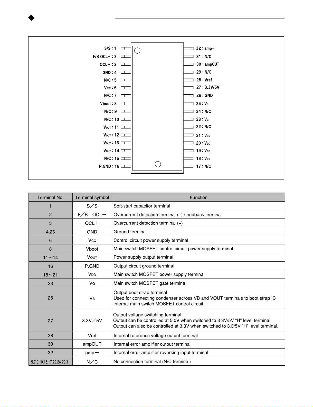
5 Terminal functions.......................................................................................4
2
-
6 Block diagrams...........................................................................................5
3. External dimensions (Diagram) ...............................................................................6
4. Characteristics .........................................................................................................7
5. Mounting .................................................................................................................8
5
-
1 Soldering pattern reference (Reflow-type)
5
-
2 Mounting cautions
5
-
3
Printed circuit board patterns and design considerations (Reference)
.............9
6. Operating instructions ..........................................................................................10
6
-
1 Basic input and output connections
6
-
2 Input protection element connection .......................................................11
6
-
3 Overvoltage protection
6
-
4 Remote ON/OFF Control Function...........................................................12
6
-
5 Reference parts .......................................................................................13
6
-
6 Electrical characteristics
7. Basic design procedure .........................................................................................14
7
-
1 Overcurrent detecting resistor (R1) selection
7
-
2 Inductance (L1) selection
7
-
3 Output capacitor selection ......................................................................15
7
-
4 Input capacitor selection
7
-
5 Thermal management
8. Electrical measurement data...........................................................................16
~
19
8
-
1 Output voltage - 3.3V
8
-
2 Output voltage - 5V
9. Packing conditions ...............................................................................................20
9
-
1 Taping type
9
-
2 Package configuration
9
-
3 Order quantity and dimensions

3
2
General description of the DC to DC Converter Power IC MD1320N
The MD1320N is a non-isolated step-down DC to DC converter power IC with built-in main switch MOSFET and SBD
flywheel. The maximum output is 7.5W (5V, 3.5A). The highly efficient power IC can be used over a wide range of
applications. Furthermore, the output switching function permits optional selection of 3.3 and 5V.
The use of a surface mounted type SSOP-32 package permits controls with minimal externally mounted parts. As a
result, the overall size of DC-DC converter power IC as a power supply unit is reduced and made as thin as possible.
Input voltage range: 8
~
30V
Output voltage: 3.3V/5V (Output switching function permits optional selection of output voltages)
Maximum output current: 1.5A
Main switch MOSFET and built-in SBD flywheel
Oscillation frequency: 250 kHz (Built-in oscillator does not require external capacitors or resistors)
Overcurrent protection function
Heat protection function
Built-in low-voltage protection (UVLO) function
Information distribution equipment Telecommunications equipment
Office automation equipment Factory automation equipment (Process control)
Electronic measuring instruments Audio-video devices
Home appliances
Device name and packaging specification codes are provided. Shipping conditions are determined according to these
specifications.
Entry example: MD1320N 4072
Specification code: Shows package configuration and product name
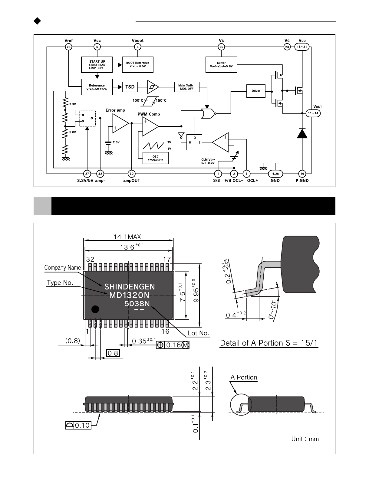
1 )Internal reference voltage (Vref)
IC internal circuitry reference voltage is provided by the temperature compensation reference voltage (5.0V). This reference
voltage (Vref) provides a maximum external output current measured at the terminal of 1 mA.
2 )Oscillation circuit (OSC)
The oscillation circuit is built into the device. No external oscillation capacitor nor resistor is required. The oscillation
frequency (250 kHz) is set internally and has a sawtooth wave pattern. The sawtooth wave pattern cannot be outputted
externally.
3 )Error amplifier (Error Amp.)
The error amplifier senses the DC to DC converter voltage and provides a PWM control signal output. Loop gain
between the error amplifier ampOUT terminal and the negative amp terminal is determined by the connections between
the feedback resistor and the capacitor. This provides stable loop compensation throughout the system.
4 )Overcurrent sensor (OCL)
The OCL is a pulse-by-pulse overcurrent sensor. The voltage drop across the external current sensing resistor is
measured between the negative and positive terminals of the OCL. If the voltage drop exceeds 0.19V, the main
switch (MOSFET) opens.
2
-
1 Features
2
-
2 Applications
2
-
3 Nomenclature
2
-
4 Peripheral functions
..
4
2
-
5 Terminal functions
5
3External dimensions(Diagram)(SSOP-32)
2
-
6 Block diagrams
6
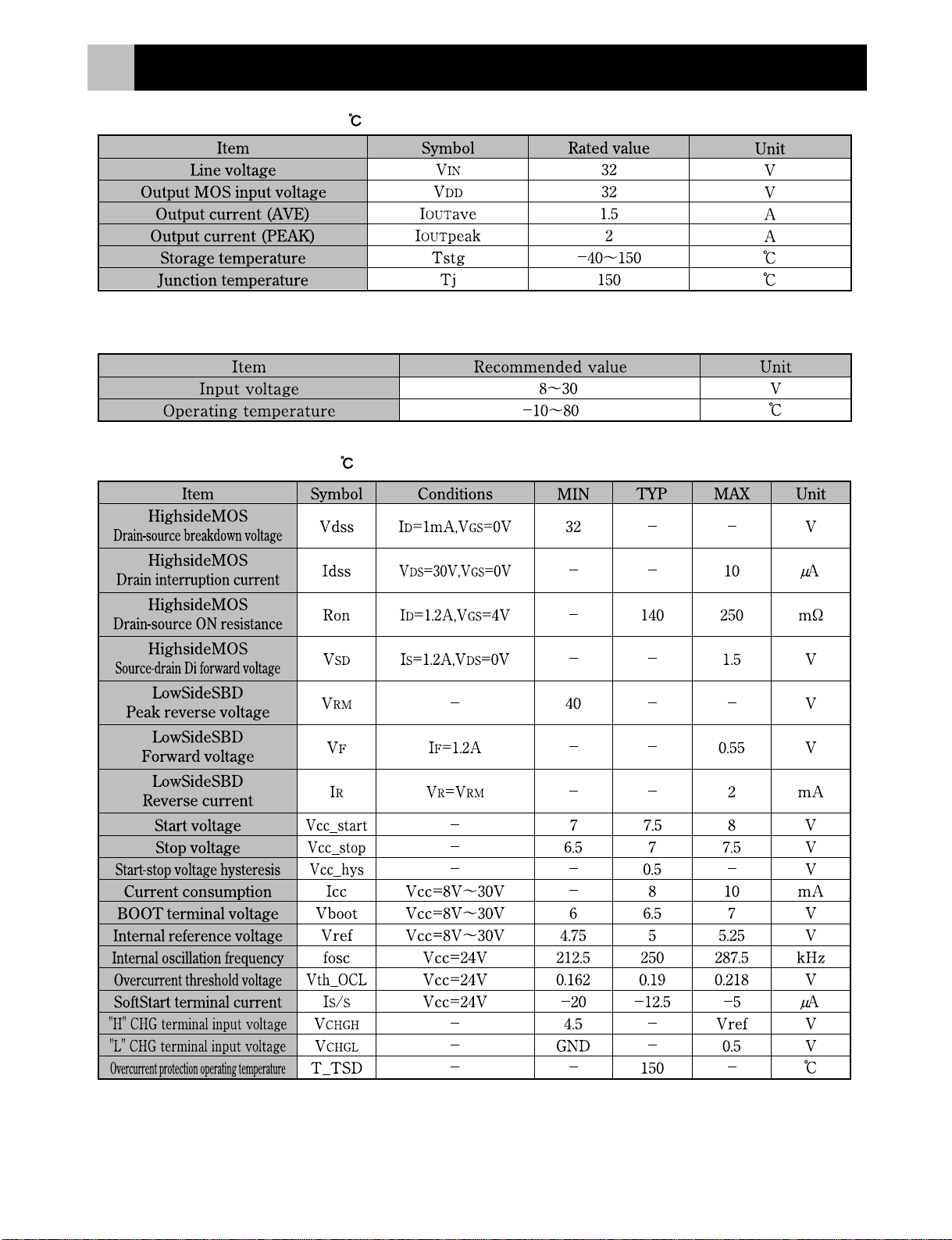
2 )Recommended operating conditions
3 )Electrical characteristics (Ta=25 )
4Characteristics
1 )Absolute maximum rating (Ta=25 )

7
1 )Mounting
Vibration and other mechanical disturbances
can exert stress on the internal parts of the
device. Carefully examine your equipment and
place the device where vibration and other
shock is minimal.
2 )Soldering cautions
Infrared reflow method
This method provides very high temperature
soldering. The chart at the right shows the
recommended temperature profiles for the
Infrared reflow soldering method.
Soldering iron
When using a soldering iron, observe the
following.
Soldering iron temperature: Not to exceed
300
Soldering iron contact time: Not to exceed 5
seconds
3 )Cleaning cautions
Carefully remove all flux. Allow time for the soldered areas to completely dry before using the device.
4 )Secondary mold cautions
After installation of the device to a board, remolding using plastic may be required. During this process, stress on the
device will depend on the type of plastic used. The best plastic (that which causes the least stress on the device) has a
minimum contraction ratio and high flexibility. Hardening temperatures should not exceed the storage temperature.
Carefully check the plastic characteristics before use.
Static electricity can damage the device. The person and clothing of personnel working with the device
should be grounded to prevent the build-up of static electricity. It is recommended that personnel stand
on rubber mats (electrical safety mats) having a resistance greater than 1M when working with the
device. This will prevent damage to the device from static electricity discharge and protect the personnel
form electrical shock.
5Mounting
0.5
9.53
1.4
0.8
(Figure 5-A)
5
-
1 Soldering pattern reference (Reflow-type)
5
-
2 Mounting cautions
8
The device does not have a voltage surge protection circuit or an input fuse. The user should install an input fuse to protect the device and
equipment before using the device.
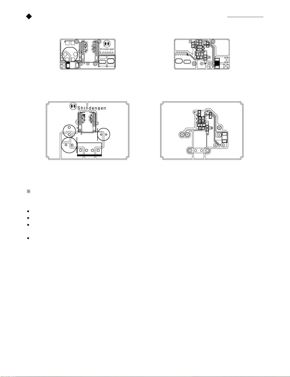
For optimum thermal efficiency, maintain the copper foil pattern as much as possible.
Connect the F/B OCL negative terminal (Pin 2) as close as possible to the output capacitor (C5).
Connect the input capacitor (C1), output capacitor (C5), choke (L1), and dropping resistor (R2) as close as possible to the power IC
device.
Separate the ground terminals (Pin 4 and Pin 26) and the P and ground terminals (Pins 16). Connect each of them as close as possible
to output capacitor (C5).
C6
R3 R1 C2
C3 C4 R2
D1KD1K
3.3V5V
MDMD
L1
C1-1 C1-2
+Vo +VinG
IC1 MD
L1
C1-1 C1-2
+Vo +VinG
C5
IC1
C6
R3 R1 C2
C3 C4 R2
3.3V5V
D1K
C5
R1
R2
C2C2
3.3V5V
D1K
C3C3 C4C4
L1
IC1
CN1
C1
MD
C5 +Vo +VinG
L1
IC1
CN1
C1
MD
C5 +Vo +VinG
R1
R2
C2
3.3V5V
D1K
C3 C4
Typical 1.5A lead parts model
Typical 1.5A surface mounted parts model
5
-
3
Printed circuit board patterns and design considerations(Reference)

9
6Operating instructions
The MD1320N power IC device uses chopper circuitry and can be referred to as a chopper type DC to DC
converter. The device requires an external choke and capacitor to be connected to it. The characteristics of
these external parts and the way they are packaged and connected will greatly affect the performance of the
device and its circuits. Carefully select these external parts to provide optimum device performance.
Neither the device input side nor output side is isolated.
Power IC device connection and use involves the rated output voltage and the maximum current output range.
1 ) If an output voltage of 3.3V is required, connect Pins 27 and 28. If an output voltage of 5V is required, connect Pins 26
and 27.
2 ) Pin 23 is the test terminal and must be left open.
3 ) Pins 5, 7, 9, 10, 15, 17, 22, 24, 29, and 31 are internal non-connecting pins (N/C terminals).
4 ) Figure 6-A shows the external parts and their connections. Be sure to prepare and connect these items before using the
device.
5 ) Output capacitor (C5) minimizes switching frequency ripple and provides a smooth and stable output voltage. The use of
a low-impedance capacitor is recommended (low impedance provides minimum ripple).
Standard connections (Figure 6-A)
6
-
1 Basic input and output terminal connections

10
Caution
The MD1320N device has an output current drop function. In the event of power IC device malfunction resulting in
excessive input current flow, smoke and flame may be emitted from the equipment. To prevent this, install a fuse or
protective circuitry to the power IC device input line.
Install the fuse or protective circuitry to the positive side of the input line(Figure 6-2, DC input). Be sure that the fuse or
protective circuitry is not too large to effectively protect the circuitry (the input line must be capable of carrying enough
current to blow the fuse).
The MD1320N power IC device does not have an overvoltage (voltage surge) protection function. If a malfunction occurs in
the device internal circuitry, there may be a voltage surge. Output will reflect this surge and damage to equipment may result.
Smoke and flame may be emitted from the equipment. To prevent this, be sure to install voltage surge sensing and
protection circuitry.
There are a number of ways to protect against voltage surge. Figure 6-B shows a typical voltage surge protection set-up. The
voltage surge sensing and protection circuit should be installed as close as possible to the load (away from the output
smoothing capacitor).
+
R1
Load
DC to DC converter
power supply
Circuit protection elements (fuses, etc.)
Overvoltage protection circuit
D2
C1
D1F1
DC
THY1
R2-
Reference part example (Figure 6-B)
6
-
2 Input protection element connection
6
-
3 Overvoltage protection

11
MD1320N
VOUT
GND
VDDVCC
R1 Q1
Q2
Q3
R2
R4
R3
DC input
R/C
G
+Vin +Vo
The MD1320N is not provided with remote ON/OFF control functions. When necessary, be sure to add the recommended
circuit shown below. The use of remote control (R/C) circuit turns the output ON and OFF without making or breaking the
input. The R/C circuit can also be employed in systems such as sequence control for a power supply system.
1) R/C terminal When turning ON power supply on the low side (connection to ground), be sure to add the circuit shown in
Fig. 6 - C, and turn the power supply OFF when the R/C circuit is on the high side.
2) R/C terminal When turning ON power supply on the high side (open), be sure to add the circuit shown in Fig. 6-D, and
turn power supply OFF when the R/C terminal is on the low side.
(Figure 6-C)
MD1320N
VOUT
GND
VDDVCC
R1 Q1
Q2
R2
R3
DC input
R/C
G
+Vin +Vo
(Figure 6-D)
6
-
4 Remote ON/OFF Control

12
Efficiency and ripple are measured according to external reference parts circuit configuration that is based on standard circuit
configuration.
Efficiency and ripple voltage conditions: Vin = 12V and Io = rated output current
6
-
5 Reference parts used with standard circuits
6
-
6 Electrical characteristics (Ta = 25 )

13
7Basic device set-up standards
Set-up sequence below
Areas that must be carefully considered in the set-up of the device include the overcurrent detecting resistor,
circuit inductance, output capacitor, input capacitor, and thermal characteristics.
Detects a peak voltage across the resistor of 0.19V+
-
15%
VR
R1= [ ]
IR
Switching noise and other factors may cause some variation in the calculated drop point value. Check your own
equipment and calculate the value accordingly.
VR : Average voltage level
IR: Drop point
The selected inductance sets the cut-off current at 15% of the rated output current.
L1= [H]
Vi (max) = Maximum input voltage
VO: Output voltage
VF : SBD flywheel forward voltage (0.5V)
I : Cut-off current 2 ( IO0.15 2) (Cut-off current flows through the choke coil. Current value is intermittent.)
f : Oscillation frequency (250 kHz)
IO : Output current
Calculated inductance values (L1) shown here represent those used in previously manufactured devices and may not be
applicable to your device. The use of an actual value somewhat higher than the measured value is standard procedure.
However, actual values lower than the measured value may be used where the rated current is low. Use the formula to back-
calculate the I using the selected L1 value. The recommended value is 0.2 IOI 0.4 IO(Cut-off at 10 to 20
percent).
7
-
1 Overcurrent detecting resistor (R1) selection
7
-
2 Inductance (L1) selection
( Vi (max)
-
Vo) ( Vo + VF)
I ( Vi (max) + VF) f
14
If an electrolytic capacitor is used, output ripple is determined by I and capacitor impedance. Use the formula below to
calculate the value. Select a device providing an impedance (ZC) lower than the calculated value.
Vrip
ZC[ ]
I
Vrip : Output ripple voltage (Ex: 25m VP
-
P)
I : Cut-off current 2
A large ripple current flows through the input capacitor. Use the formula below to calculate the value. Select a device
providing a higher ripple current capacity (Irip) than the calculated value.
VO +VF
D= Vi (min)+VF
Irip D (1
-
D) IO[A]
D : Duty
VO : Output voltage
Vi (min) : Minimum input voltage
VF : SBD flywheel forward voltage (0.5V)
IO : Output current
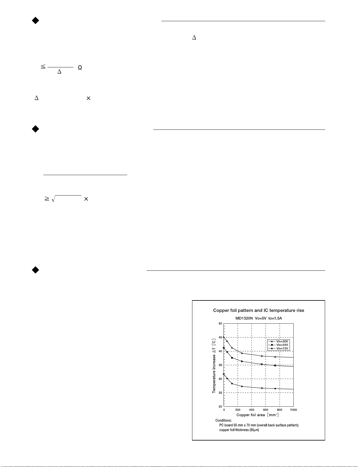
The MD1320N is so designed that heat is radiated when Pins 11, 12, 13, 14, and Pins 18, 19, 20 and 21 are connected to the
substrate pattern. The necessary area of heat radiation pattern
differs according to the material and size, but be sure to check
with an actually operating piece of equipment and referring to
the data given in Fig. 7 - A.
Since the temperature rise also differs according to the
conditions of I/O voltage and output current, use 105 degrees
maximum as the design target for the surface temperature of
case.
Figure 7-A
7
-
3 Output capacitor selection
7
-
4 Input capacitor selection
7
-
5 Thermal management

15
8Electrical data measurement
This data results from measurements taken using equipment connected as shown in the standard connection
diagram and using reference part and reference circuitry patterns.
8
-
1 Output voltage - 3.3V
Line regulation Load regulation
Temperature drift Efficiency and loss characteristics
IC temperature increase Derating curve
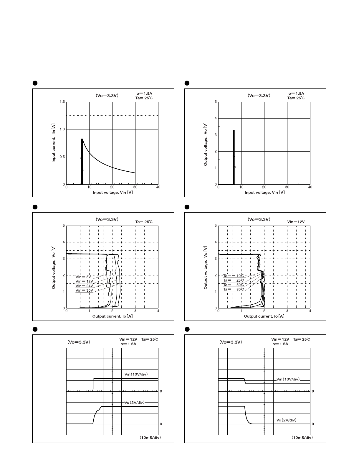
16
Input curreent/input voltage characteristics Input voltage/output voltage characteristics
Current limit characteristic (Input fluctuation)
Current limit characteristic (Temperature fluctuation)
Start-up rising characteristics Shut-down falling characteristics
17
Line regulation Load regulation
Temperature drift Efficiency and loss characteristics
IC temperature increase Derating curve
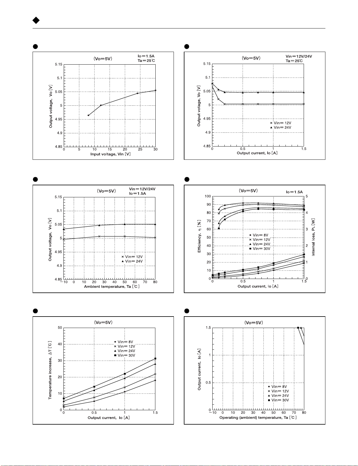
8
-
1 Output voltage - 5V

18
Input curreent/input voltage characteristics Input voltage/output voltage characteristics
Current limit characteristic (Input fluctuation)
Current limit characteristic (Temperature fluctuation)
Start-up rising characteristics Shut-down falling characteristics
19
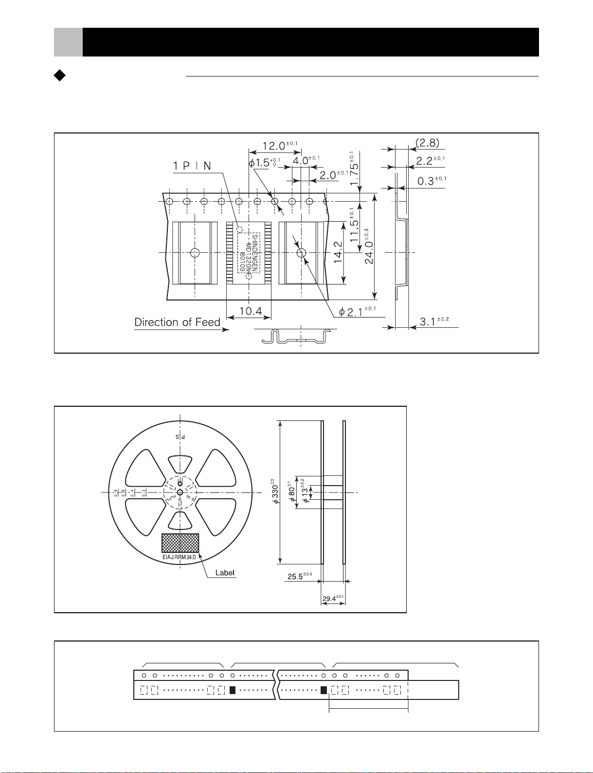
9Packing
1 )Tape
.Material : PVC
.Dimensions Comply with JIS, C-0806
2 )Reel
.Material : Polystyrene
.Demensions Comply with EIAJ, ETX-7001
.Label
Type No.
Code No.
Date Code
Quantity
Manufacturer
3 )Leader and Trailer
Trailer 120mm(min)
Leader 120mm(min)
Top cover 400mm(min)Device
9
-
1 Tape & Reel
Table of contents
Other Shindengen Media Converter manuals


