TABLE OF CONTENTS
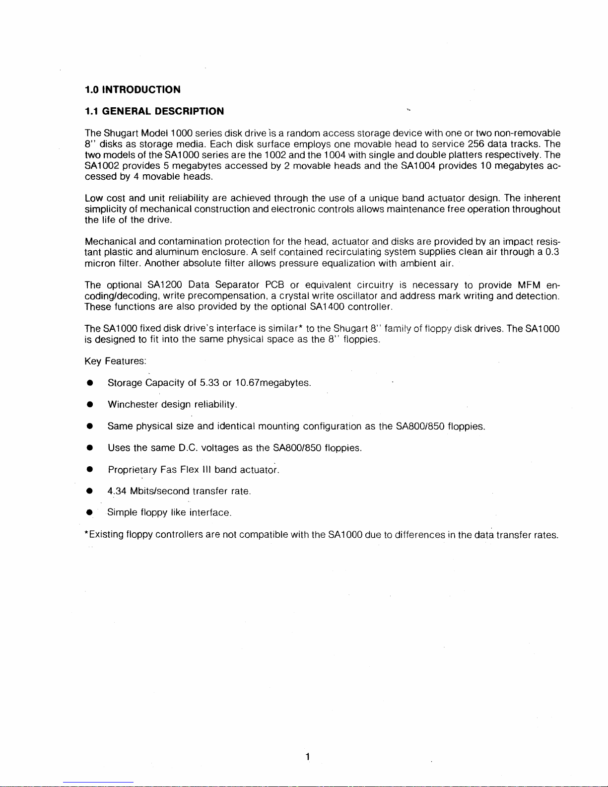
1.0 Introduction
.....................................................................
.
1.1
General Description
..
. . . . . . . . . . . . . . . . . . . . . . . . . . . . . . . . . . . . . . . . . . . . . . . . . . . . . . . . .
..
1
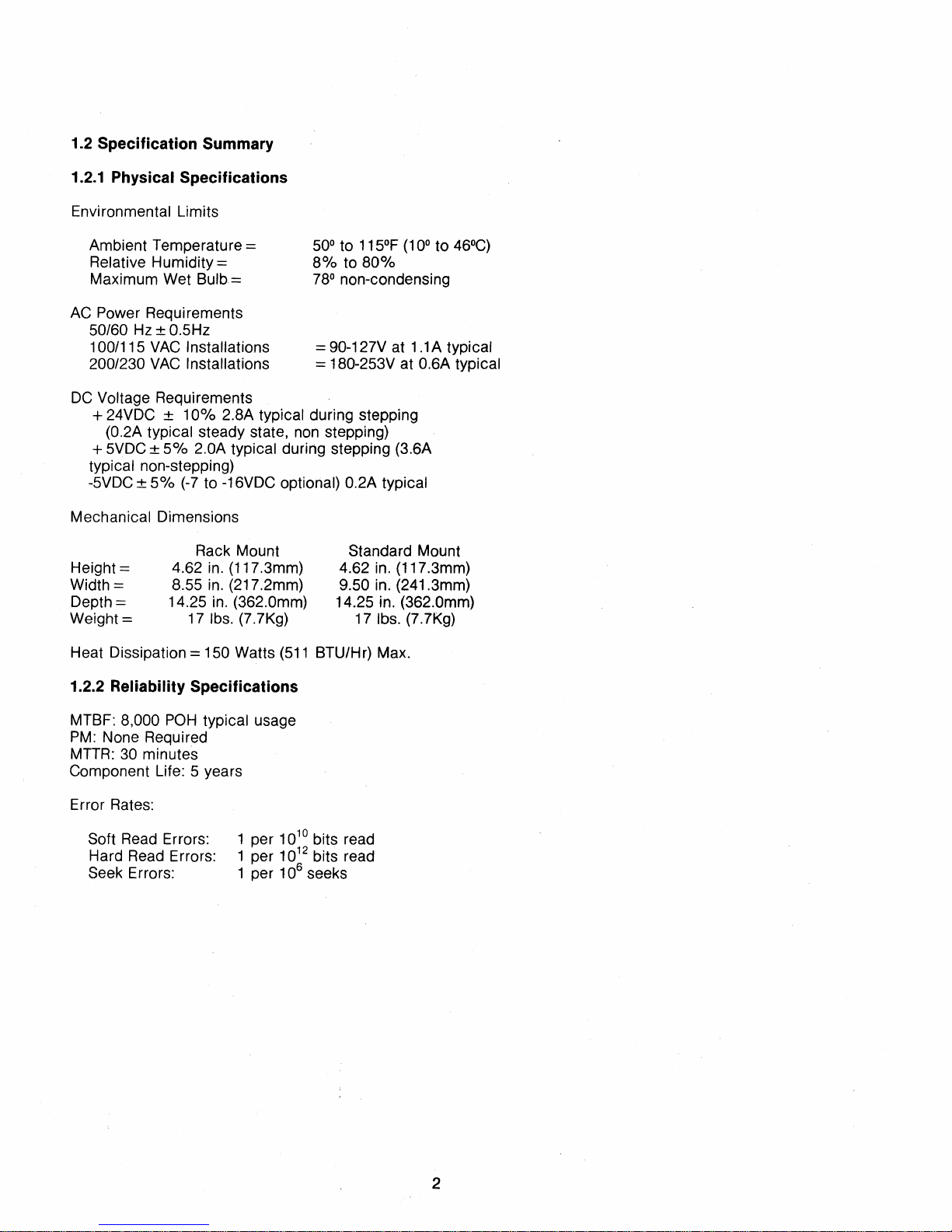
1.2 Specification Summary. . . . . . . . . . . . . . . . . . . . . . . . . . . . . . . . . . . . . . . . . . . . . . . . . . . . . . . . .
..
2
1.2.1
Physical Specifications
................................
. . . . . . . . . . . . . . . . . . . . . . .
..
2
1.2.2 Reliability Specifications
..
. . . . . . . . . . . . . . . . . . . . . . . . . . . . . . . . . . . . . . . . . . . . . . . . . . . .
..
2
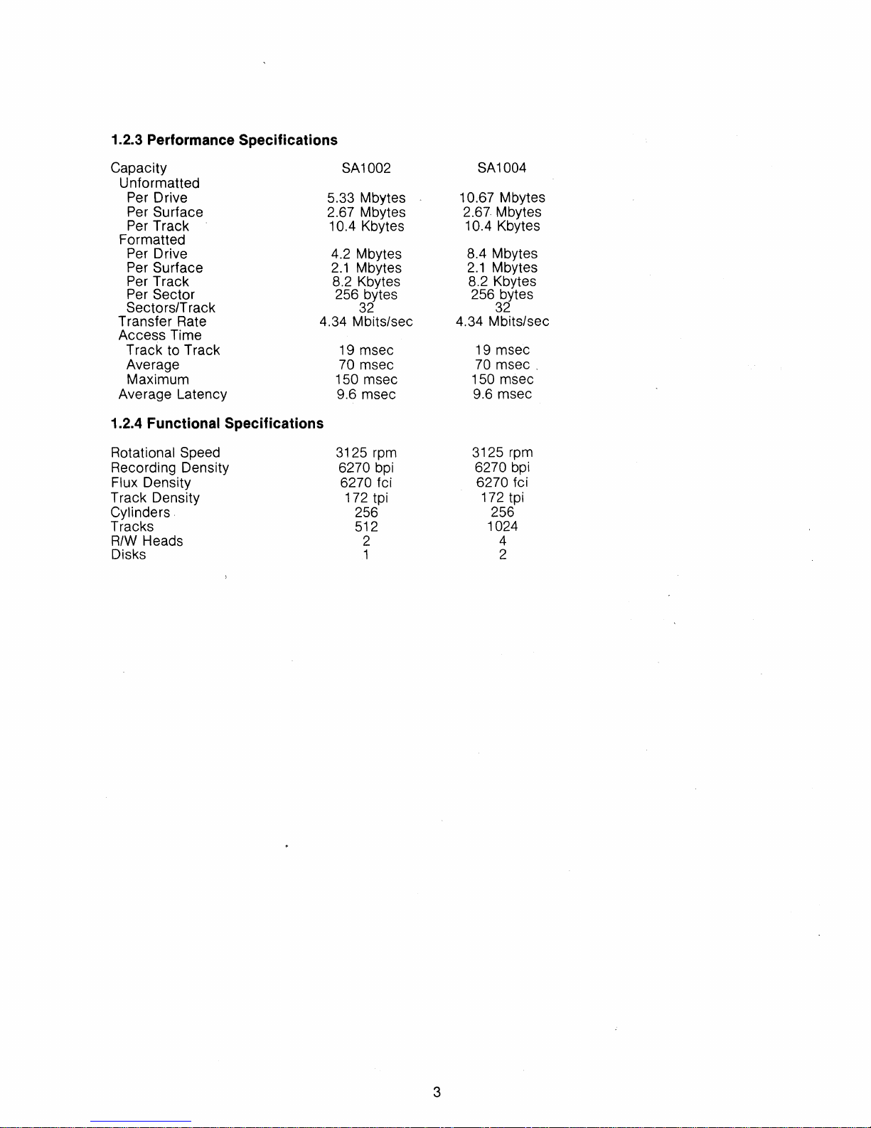
1.2.3 Performance Specifications. . . . . . . . . . . . . . . . . . . . . . . . . . . . . . . . . . . . . . . . . . . . . . . . . . . .
..
3
1.2.4 Functional Specifications. . . . . . . . . . . . . . . . . . . . . . . . . . . . . . . . . . . . . . . . . . . . . . . . . . . . . .
..
3
2.0 Functional Characteristics. . . . . . . . . . . . . . . . . . . . . . . . . . . . . . . . . . . . . . . . . . . . . . . . . . . . . . . . .
..
4
2.1
General Operation. . . . . . . . . . . . . . . . . . . . . . . . . . . . . . . . . . . . . . . . . . . . . . . . . . . . . . . . . . . . .
..
4
2.2 Read/Write and Control Electronics
........
. . . . . . . . . . . . . . . . . . . . . . . . . . . . . . . . . . . . . . .
..
4
2.3 Drive Mechanism
.....................................................
: . . . . . . .
..
5
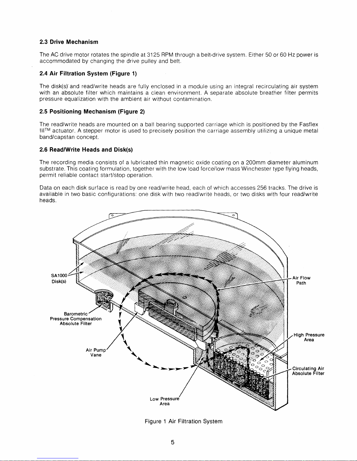
2.4 Air Filtration System (Figure
1)
. . . . . . . . . . . . . . . . . . . . . . . . . . . . . . . . . . . . . . . . . . . . . . . . . . .
..
5
2.5 Positioning Mechanism (Figure
2)
. . . . . . . . . . . . . . . . . . . . . . . . . . . . . . . . . . . . . . . . . . . . . . . . .
..
5
2.6 Read/Write Heads and Disk(s). . . . . . . . . . . . . . . . . . . . . . . . . . . . . . . . . . . . . . . . . . . . . . . . . . . .
..
5
3.0 Functional Operations . . . . . . . . . . . . . . . . . . . . . . . . . . . . . . . . . . . . . . . . . . . . . . . . . . . . . . .
..
7
3.1
Power Sequencing
..............................................................
7
3.2 Drive Selection . . . . . . . . . . . . . . . . . . . . . . . . . . . . . . . . . . . . . . . . . . . . . . .
..
. . . . . . . . . . . . . .
..
7
3.3 Track Accessing
................................
'.
. . . . . . . . . . . . . . . . . . . . . . . . . . . . .
..
7
3.4 Head Selection . . . . . . . . . . . . . . . . . . . . . . . . . . . . . . . . . . . . . . . . . . . . . . . . . . . . . . . . . . . . . . .
..
7
3.5
Read
Operation. . . . . . . . . . . . . . . . . . . . . . . . . . . . . . . . . . . . . . . . . . . . . . . . . . . . . . . . . . . . . . .
..
7
3.6 Write Operation
...........................................
'.
. . . . . . . . . . . . . . . . . . .
..
8
4.0 Electrical Interface .
J.
. . . . . . . . . • • • • . • . . . • • . • . • • • • . . • . . . . • • • . . . . . . . . • • . . . . . . . • • . . . • •
..
8
4.1
Signal Interface . . . . . . . . . . . . . . . . . . . . . . . . . . . . . . . . . . . . . . . . . . . . . . . . . . . . . . . . . . . . . . .
..
8
4.1.1
Control Input Lines
.....................................................
"
.......
10
4.1.1.1
DriveSelect1-4
.............................................................
10
4.1.1.2 Direction
In
.................................................................
10
4.1.1.3 Step
.......................................................................
11
4.1
.1.4 Head Select 2° and
21
.........................................................
12
4.1.1.5 Write Gate
...
,
..............................................................
12
4.1.1.6 Reduced Write Current
........................................................
12
4.1.2 Control Output Lines
............................................................
13
4.1.2.1 Track 000
...................................................................
13
4.1.2.2 Index
......................................................................
13
4.1.2.3 Ready
............................................................
13
4.1.2.4 Write Fault. . . . . . . . . . . . . . . . . . . . . . . . . . . . . . . . . . . . . . . . . . . . . . . . . . . .
.......
14
4.1.2.5 Seek Complete
..............................................................
14
4.1.3 Data Transfer Lines . . . . . . . . . . . . . . . . . . . . . . . . . . . . . . . . . . . . . . . . . . . . . . . . . . .
......
14
4.1.3.1 MFM Write Data
......
'
.......................................................
15
4.1.3.2 MFM Read Data
.............................................................
15
4.1.3.3 Timing Clock
................................................................
16
4.1.4 Select Status
.................................................................
16
4.1.5 General Timing Requirements
....................................................
17
4.2 Power Interface
.................................................................
17
4.2.1
AC
Power
....................................................................
17
4.2.2
DC
Power
....................................................................
17
5.0 Physical Interface
..................................................................
19
5.1
J1/P1
Connector
................................................................
20
5.2 J2/P2 Connector
................................................................
20
5.3 J4/P4 Connector
...........................................................
21
5.4 J5/P5 Connector
..........................................................
21