Silicon Laboratories Si5341 User manual
Preliminary Rev. 0.9 7/14 Copyright © 2014 by Silicon Laboratories Si5341/40
This information applies to a product under development. Its characteristics and specifications are subject to change without notice.
Si5341/40
LOW-JITTER, 10-OUTPUT, ANY-FREQUENCY, ANY-OUTPUT
CLOCK GENERATOR
Features
Applications
Description
The any-frequency, any-output Si5341/40 clock generators combine a wide-band
PLL with proprietary MultiSynth fractional synthesizer technology to offer a
versatile and high performance clock generator platform. This highly flexible
architecture is capable of synthesizing a wide range of integer and non-integer
related frequencies up to 800 MHz on 10 differential clock outputs while
delivering sub-100 fs rms phase jitter performance and 0 ppm error. Each of the
clock outputs can be assigned its own format and output voltage enabling the
Si5341/40 to replace multiple clock ICs and oscillators with a single device
making it a true “clock tree in a chip”.
The Si5341/40 can be quickly and easily configured using ClockBuilder Pro
software. Custom part numbers are automatically assigned using a
ClockBuilderPro for fast, free, and easy factory programming, or the Si5341/40
can be programmed in-circuit via I2C and SPI serial interface.
Generates free-running or
synchronous output clocks
MultiSynth™ technology enables
any-frequency synthesis on any-
output with 0 ppm frequency
accuracy with respect to the input
Highly configurable outputs
compatible with LVDS, LVPECL,
LVCMOS, HCSL, or programmable
voltage swing and common mode
Excellent jitter: <100 fs RMS typ
Input frequency range:
External crystal: 25, 48-54 MHz
Differential clock: 10 to 750 MHz
LVCMOS clock: 10 to 250 MHz
Output frequency range:
Differential: 100 Hz to 800 MHz
LVCMOS: 100 Hz to 250 MHz
Output-output skew: <100 ps
Adjustable output-output delay
Optional zero delay mode
Independent glitchless on-the-fly
output frequency changes
DCO mode with frequency
increment and decrement as low as
0.001 ppb/step
Core voltage:
VDD: 1.8 V ±5%
VDDA: 3.3 V ±5%
Independent output supply pins:
3.3V, 2.5V, or 1.8V
Built-in power supply filtering
Status monitoring: LOS, LOL
Serial Interface: I2C or SPI (3-wire
or 4-wire)
In-circuit programmable with non-
volatile OTP memory (2x
programmable)
ClockBuilder ProTM software utility
simplifies device configuration and
assigns customer part numbers
Si5341: 4 input, 10 output, 64 QFN
Si5340: 4 input, 4 output, 44 QFN
Temperature range: –40 to +85 °C
Pb-free, RoHS-6 compliant
Clock tree generation replacing
XOs, buffers, signal format
translators
Any-frequency synchronous clock
translation
Clocking for FPGAs, processors,
memory
Ethernet switches/routers
OTN framers/mappers/processors
Test equipment & instrumentation
Broadcast video
Ordering Information:
See section 7
Pin Assignments
GND
Pad
IN1
IN1
IN_SEL0
IN_SEL1
SYNC
RST
X1
XA
XB
X2
OE
INTR
VDDA
IN2
IN2
SCLK
A0/CS
SDA/SDIO
A1/SDO
VDD
RSVD
RSVD
VDDO0
OUT0
OUT0
FDEC
OUT1
OUT1
VDDO2
OUT2
OUT2
FINC
LOL
VDD
OUT6
OUT6
VDDO6
OUT5
OUT5
VDDO5
I2C_SEL
OUT4
OUT4
VDDO4
OUT3
OUT3
VDDO3
VDDO7
OUT7
OUT7
VDDO8
OUT8
OUT8
OUT9
OUT9
VDDO9
VDD
FB_IN
FB_IN
IN0
IN0
1
2
3
4
5
6
7
8
9
10
11
12
13
14
15
16
48
47
46
45
44
43
42
41
40
39
38
37
36
35
34
33
17
18
19
20
21
22
23
24
25
26
27
28
29
30
31
32
64
63
62
61
60
59
58
57
56
55
54
53
52
51
50
49
VDDO1
Si5341 64QFN
Top View
RSVD
RSVD
GND
Pad
IN1
IN1
IN_SEL0
INTR
X1
XA
XB
X2
OE
RST
VDDA
VDDA
IN2
A0/CS
SDA/SDIO
A1/SDO
OUT0
OUT0
VDDO0
SCLK
I2C_SEL
OUT1
OUT1
VDDO1
VDDO3
OUT3
OUT3
FB_IN
FB_IN
IN0
IN0
Si5340 44QFN
Top View
1
2
3
4
5
6
7
8
9
10
33
32
31
30
29
28
27
26
25
24
12
13
14
15
16
17
18
19
20
21
44
43
42
41
40
39
38
37
36
35
VDD
OUT2
OUT2
VDDO2
VDDS
LOL
LOS_XAXB
VDD
IN_SEL1
IN2 11 23
NC 22
VDD
VDD
34

Si5341/40
2 Preliminary Rev. 0.9
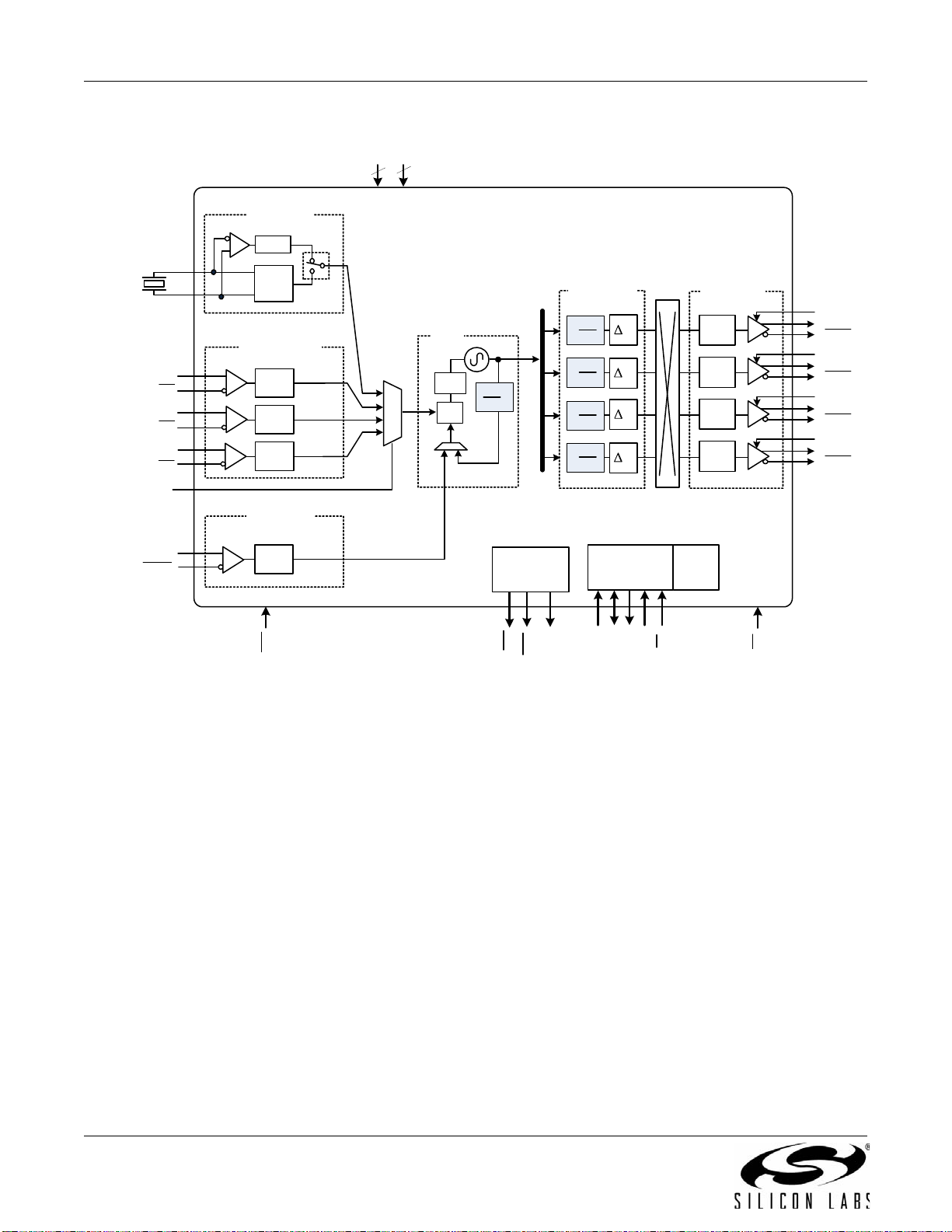
Functional Block Diagram
Si5341/40
FB_IN
IN0
IN_SEL
IN1
IN2
XB
XA
XTAL
÷INT
÷INT
÷INT
OSC
Multi
Synth OUT0
÷INT
OUT1
÷INT
OUT2
÷INT
OUT3
÷INT
OUT4
÷INT
OUT5
÷INT
OUT6
÷INT
OUT7
÷INT
OUT8
÷INT
OUT9
÷INT
Multi
Synth
Multi
Synth
Multi
Synth
Multi
Synth
Si5340 Si5341
PLL
÷INT
NVM
I2C/SPI
Control/
Status

Si5341/40
Preliminary Rev. 0.9 3
TABLE OFCONTENTS
1. Typical Application Schematic . . . . . . . . . . . . . . . . . . . . . . . . . . . . . . . . . . . . . . . . . . . . . .4
2. Electrical Specifications . . . . . . . . . . . . . . . . . . . . . . . . . . . . . . . . . . . . . . . . . . . . . . . . . . .5
3. Detailed Block Diagrams . . . . . . . . . . . . . . . . . . . . . . . . . . . . . . . . . . . . . . . . . . . . . . . . . .19
4. Functional Description . . . . . . . . . . . . . . . . . . . . . . . . . . . . . . . . . . . . . . . . . . . . . . . . . . .21
4.1. Modes of Operation . . . . . . . . . . . . . . . . . . . . . . . . . . . . . . . . . . . . . . . . . . . . . . . . . .21
4.2. Frequency Configuration . . . . . . . . . . . . . . . . . . . . . . . . . . . . . . . . . . . . . . . . . . . . . .22
4.3. Inputs . . . . . . . . . . . . . . . . . . . . . . . . . . . . . . . . . . . . . . . . . . . . . . . . . . . . . . . . . . . .22
4.4. Fault Monitoring . . . . . . . . . . . . . . . . . . . . . . . . . . . . . . . . . . . . . . . . . . . . . . . . . . . .24
4.5. Outputs . . . . . . . . . . . . . . . . . . . . . . . . . . . . . . . . . . . . . . . . . . . . . . . . . . . . . . . . . . .25
4.6. Power Management . . . . . . . . . . . . . . . . . . . . . . . . . . . . . . . . . . . . . . . . . . . . . . . . .29
4.7. In-Circuit Programming . . . . . . . . . . . . . . . . . . . . . . . . . . . . . . . . . . . . . . . . . . . . . . .29
4.8. Serial Interface . . . . . . . . . . . . . . . . . . . . . . . . . . . . . . . . . . . . . . . . . . . . . . . . . . . . .29
4.9. Custom Factory Preprogrammed Parts . . . . . . . . . . . . . . . . . . . . . . . . . . . . . . . . . .29
5. Register Map . . . . . . . . . . . . . . . . . . . . . . . . . . . . . . . . . . . . . . . . . . . . . . . . . . . . . . . . . . . .30
5.1. Addressing Scheme . . . . . . . . . . . . . . . . . . . . . . . . . . . . . . . . . . . . . . . . . . . . . . . . .30
5.2. High-Level Register Map . . . . . . . . . . . . . . . . . . . . . . . . . . . . . . . . . . . . . . . . . . . . . .30
6. Pin Descriptions . . . . . . . . . . . . . . . . . . . . . . . . . . . . . . . . . . . . . . . . . . . . . . . . . . . . . . . . .32
7. Ordering Guide . . . . . . . . . . . . . . . . . . . . . . . . . . . . . . . . . . . . . . . . . . . . . . . . . . . . . . . . . .39
8. Package Outlines . . . . . . . . . . . . . . . . . . . . . . . . . . . . . . . . . . . . . . . . . . . . . . . . . . . . . . . .40
8.1. Si5341 9x9 mm 64-QFN Package Diagram . . . . . . . . . . . . . . . . . . . . . . . . . . . . . . .40
8.2. Si5340 7x7 mm 44-QFN Package Diagram . . . . . . . . . . . . . . . . . . . . . . . . . . . . . . .41
9. PCB Land Pattern . . . . . . . . . . . . . . . . . . . . . . . . . . . . . . . . . . . . . . . . . . . . . . . . . . . . . . . .42
10. Top Marking . . . . . . . . . . . . . . . . . . . . . . . . . . . . . . . . . . . . . . . . . . . . . . . . . . . . . . . . . . .44
11. Device Errata . . . . . . . . . . . . . . . . . . . . . . . . . . . . . . . . . . . . . . . . . . . . . . . . . . . . . . . . . .45
Appendix—Advance Product Information Revision History . . . . . . . . . . . . . . . . . . . . . . .46
Contact Information . . . . . . . . . . . . . . . . . . . . . . . . . . . . . . . . . . . . . . . . . . . . . . . . . . . . . . . .48
Si5341/40
4 Preliminary Rev. 0.9
1. Typical Application Schematic
Figure 1. Using The Si5341 to Replace a Discrete Clock Tree
PCB Clock Tree
Level
Translator
Clock
Generator
161.1328125
MHz
Buffer
133.33 MHz
Buffer
One Si5341 replaces:
3x crystal oscillators (XO)
4x buffers
1x clock generator
2x level translators
1x delay line
“Clock Tree
On-a-Chip”
XA
XB
25 MHz 4x 200 MHz
2.5V LVCMOS
2x 161.1328125 MHz
LVDS 2x 133.33 MHz
1.8V LVCMOS
Buffer
125 MHz
Level
Translator
Buffer
Delay Line
4x 125 MHz
3.3V LVCMOS
3x 125 MHz
LVPECL
Si5341 Nn0
Nd0
LPF
PD
PLL
÷Mn
Md
Free Run
Mode
OSC
Nn1
Nd1
t2
N2n
N2d
N3n
N3d
N4n
N4d
161.1328125MHz
133.33MHz
125MHz
XA
XB
125MHz
200MHz
1x 161.1328125 MHz
LVDS
1x 161.1328125 MHz
LVDS
2x 133.33 MHz
1.8V LVCMOS
2x 125 MHz
3.3V LVCMOS
2x 125 MHz
3.3V LVCMOS
2x 200 MHz
2.5V LVCMOS
2x 200 MHz
2.5V LVCMOS
1x 125 MHz
LVPECL
1x 125 MHz
LVPECL
1x 125 MHz
LVPECL
25 MHz

Si5341/40
Preliminary Rev. 0.9 5
2. Electrical Specifications
Table 1. Recommended Operating Conditions
(VDD =1.8V±5%,V
DDA =3.3V±5%,T
A= –40 to 85 °C)
Parameter Symbol Min Typ Max Units
Ambient Temperature TA–402585°C
Junction Temperature TJMAX ——125°C
Core Supply Voltage VDD 1.71 1.80 1.89 V
VDDA 3.14 3.30 3.47 V
Output Driver Supply Voltage VDDO 3.14 3.30 3.47 V
2.38 2.50 2.62 V
1.71 1.80 1.89 V
*Note: All minimum and maximum specifications are guaranteed and apply across the recommended operating conditions.
Typical values apply at nominal supply voltages and an operating temperature of 25 °C unless otherwise noted.
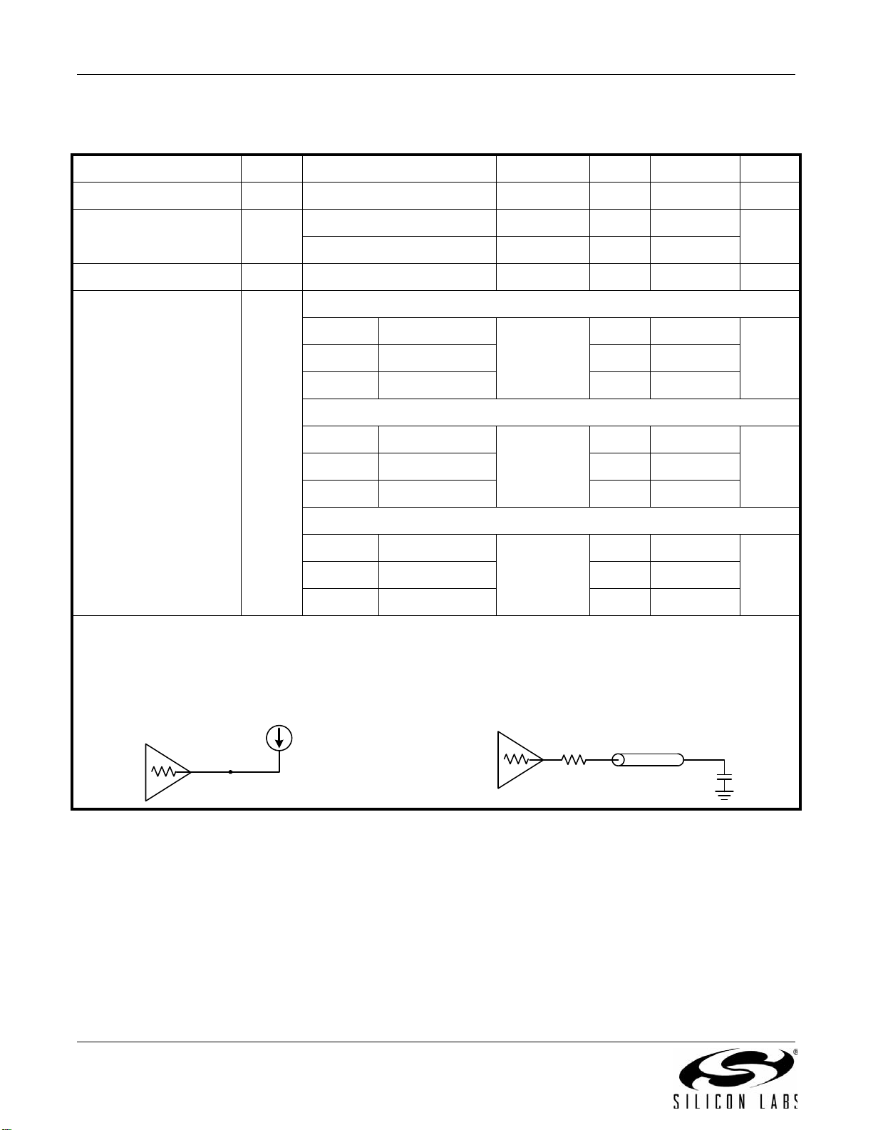
Table 2. DC Characteristics
(VDD =1.8V±5%,V
DDA =3.3V±5%,V
DDO = 1.8 V ±5%, 2.5 V ±5%, or 3.3 V ±5%, TA= –40 to 85 °C)
Parameter Symbol Test Condition Min Typ Max Units
Core Supply Current IDD Si5341 or
Si5340 Notes 1,2—98140mA
IDDA —115125mA
Output Buffer Supply Current IDDOx LVPECL Output3
@ 156.25 MHz —2325mA
LVDS Output3
@ 156.25 MHz —1618mA
3.3V LVCMOS4output
@ 156.25 MHz —1926mA
2.5 V LVCMOS4output
@ 156.25 MHz —1519mA
1.8 V LVCMOS4output
@ 156.25 MHz —1113mA
Total Power Dissipation PdSi5341 Notes 1,5— 836 945 mW
Si5340 Notes 2,5— 645 — mW
Notes:
1. Si5341 test configuration: 7 x 2.5 V LVDS outputs enabled @156.25 MHz. Excludes power in termination resistors.
2. Si5340 test configuration: 4 x 2.5 V LVDS outputs enabled @ 156.25 MHz. Excludes power in termination resistors.
3. Differential outputs terminated into an AC coupled 100 load.
4. LVCMOS outputs measured into a 6 inch 50 PCB trace with 5 pF load.
5. Detailed power consumption for any configuration can be estimated using ClockBuilderPro when an evaluation board
(EVB) is not available. All EVBs support detailed current measurements for any configuration.
50
50
100
OUT
OUT
IDDO
Differential Output Test Configuration
50
OUTa
IDDO
5 pF
LVCMOS Output Test Configuration
6 inch
OUTb

Si5341/40
6 Preliminary Rev. 0.9
Table 3. Input Specifications
(VDD =1.8V±5%,V
DDA =3.3V±5%,T
A=–40to85°C)
Parameter Symbol Test Condition Min Typ Max Units
Differential or Single-Ended - AC Coupled (IN0/IN0, IN1/IN1, IN2/IN2, FB_IN/FB_IN)
Input Frequency Range fIN_DIFF 10 — 750 MHz
Voltage Swing VIN fin < 400 MHz 100 — 1000 mVpp_se
600 MHz < fin <
800 MHz 225 — 1000 mVpp_se
fin > 800 MHz 375 — 1000 mVpp_se
Slew Rate1, 2 SR 400 — — V/µs
Duty Cycle DC 40 — 60 %
Capacitance CIN —2 — pF
LVCMOS - DC Coupled (IN0, IN1, IN2)
Input Frequency fIN_CMOS 10 — 250 MHz
Input Voltage VIL -0.1 — 0.33 V
VIH 0.80 — — V
Slew Rate1, 2 SR 400 — — V/µs
Duty Cycle DC Clock Input 40 — 60 %
Minimum Pulse Width PW Pulse Input 1.6 — — ns
Input Resistance RIN —8 — kΩ
REFCLK (Applied to XA/XB)
REFCLK Frequency fIN_REF Frequencyrange
for best output
jitter performance
48 — 54 MHz
10 — 120 MHz
Input Voltage Swing VIN 350 — 1600 mVpp_se
Slew rate1, 2 SR Imposed for best
jitter performance 400 — — V/µs
Input Duty Cycle DC 40 — 60 %
Notes:
1. Imposed for jitter performance.
2. Rise and fall times can be estimated using the following simplified equation: tr/tf80-20 = ((0.8 - 0.2) * VIN_Vpp_se) / SR.
3. VDDIO is determined by the IO_VDD_SEL bit. It is selectable as VDDA or VDD.
Si5341/40
Preliminary Rev. 0.9 7
Table 4. Control Input Pin Specifications
(VDD =1.8V±5%,V
DDA =3.3V±5%,V
DDS = 3.3 V ±5%, 1.8 V ±5%, TA= –40 to 85 °C)
Parameter Symbol Test Condition Min Typ Max Units
Si5341 Control Input Pins (I2C_SEL, IN_SEL[1:0], RST, OE, SYNC, A1, SCLK, A0/CS, FINC, FDEC)
Input Voltage VIL -0.1 — 0.3xVDDIO*V
VIH 0.7xVDDIO1—3.6 V
Input Capacitance CIN —2— pF
Input Resistance IL—20— k
Minimum Pulse Width PW RST 50 — — ns
Si5340 Control Input Pins (I2C_SEL, IN_SEL[1:0], RST, OE, A1, SDA, SDI, SCLK, A0/CS)
Input Voltage VIL –0.1 — 0.3xVDDIO*V
VIH 0.7xVDDIO*—3.6 V
Input Capacitance CIN —2— pF
Input Resistance IL—20— k
Minimum Pulse Width PW RST 50 — — ns
*Note: VDDIO is determined by the IO_VDD_SEL bit. It is selectable as VDDA or VDD.
Table 5. Differential Clock Output Specifications
(VDD = 1.8 V ±5%, VDDA = 3.3V ±5%, VDDO = 1.8 V ±5%, 2.5 V ±5%, or 3.3 V ±5%, TA= –40 to 85 °C)
Parameter Symbol Test Condition Min Typ Max Units
Output Frequency fOUT 0.0001 — 800 MHz
Duty Cycle DC f < 400 MHz 48 — 52 %
400 MHz < f < 800 MHz 45 — 55 %
Output-Output Skew TSK Differential Output — — 100 ps
OUT-OUT Skew TSK_OUT Measured from the positive
to negative output pins ——100 ps
Notes:
1. Normal swing mode, high swing mode, Vswing and Cmode settings are programmable through register settings and
can be stored in NVM. Each output driver can be programmed independently.
2. Not all combinations of voltage swing and common mode voltages settings are possible.
3. Common mode voltage min/max variation = ±4% from typical value
4. Driver output impedance depends on selected output mode (Normal, High).
5. Measured for 156.25 MHz carrier frequency. Sinewave noise added to VDDO (1.8 V = 50 mVpp, 2.5 V/
3.3 V = 100 mVpp) and noise spur amplitude measured.
OUTx
OUTx Vpp_se
Vpp_se Vpp_diff = 2*Vpp_se
Vcm
Vcm Vcm

Si5341/40
8 Preliminary Rev. 0.9
Output Voltage Swing1Normal Swing Mode
VOUT VDDO =3.3V,
2.5 V, or 1.8 V LVDS 370 470 570 mVpp_se
LVPECL 650 820 1050
High Swing Mode
VOUT VDDO =3.3V,
2.5 V, or 1.8 V LVDS 310 420 530 mVpp_se
VDDO =3.3V
or 2.5 V LVPECL 590 830 1060
Common Mode Voltage1, 2, 3 Normal Swing or High Swing Modes
VCM VDDO = 3.3 V LVDS 1.12 1.23 1.34 V
LVPECL 1.90 2.0 2.13
VDDO = 2.5 V LVPECL
LVDS 1.17 1.23 1.3
Rise and Fall Times
(20% to 80%) tR/tFNormal Swing Mode — 170 220 ps
High Swing Mode — 250 320
Differential Output Impedance4ZONormal Swing Mode — 100 —
High Swing Mode — Hi-Z —
Table 5. Differential Clock Output Specifications (Continued)
(VDD = 1.8 V ±5%, VDDA = 3.3V ±5%, VDDO = 1.8 V ±5%, 2.5 V ±5%, or 3.3 V ±5%, TA= –40 to 85 °C)
Parameter Symbol Test Condition Min Typ Max Units
Notes:
1. Normal swing mode, high swing mode, Vswing and Cmode settings are programmable through register settings and
can be stored in NVM. Each output driver can be programmed independently.
2. Not all combinations of voltage swing and common mode voltages settings are possible.
3. Common mode voltage min/max variation = ±4% from typical value
4. Driver output impedance depends on selected output mode (Normal, High).
5. Measured for 156.25 MHz carrier frequency. Sinewave noise added to VDDO (1.8 V = 50 mVpp, 2.5 V/
3.3 V = 100 mVpp) and noise spur amplitude measured.
OUTx
OUTx Vpp_se
Vpp_se Vpp_diff = 2*Vpp_se
Vcm
Vcm Vcm
Si5341/40
Preliminary Rev. 0.9 9
Power Supply Noise Rejection5PSRR Normal Swing Mode
10 kHz sinusoidal noise — –93 — dBc
100 kHz sinusoidal noise — –93 —
500 kHz sinusoidal noise — –84 —
1 MHz sinusoidal noise — –79 —
High Swing Mode
10 kHz sinusoidal noise — –98 — dBc
100 kHz sinusoidal noise — –95 —
500 kHz sinusoidal noise — –84 —
1 MHz sinusoidal noise — –76 —
Output-output Crosstalk XTALK Measured spur from adja-
cent output —–73— dBc
Table 6. Output Status Pin Specifications
(VDD =1.8V±5%,V
DDA =3.3V±5%,V
DDS = 3.3 V ±5%, 1.8 V ±5%, TA= –40 to 85 °C)
Parameter Symbol Test Condition Min Typ Max Units
Si5341 Status Output Pins (LOL, INTR)
Output Voltage VOH IOH = –2 mA VDDIO*x 0.75 — — V
VOL IOL = 2 mA — — VDDIO1x 0.15 V
Si5340 Status Output Pins (INTR)
Output Voltage VOH IOH = –2 mA VDDIO*x 0.75 — — V
VOL IOL = 2 mA — — VDDIO1x 0.15 V
Si5340 Status Output Pins (LOL, LOS_XAXB)
Output Voltage VOH IOH = –2 mA VDDS x 0.85 — — V
VOL IOL = 2 mA — — VDDS x 0.15 V
*Note: VDDIO is determined by the IO_VDD_SEL bit. It is selectable as VDDA or VDD.
Table 5. Differential Clock Output Specifications (Continued)
(VDD = 1.8 V ±5%, VDDA = 3.3V ±5%, VDDO = 1.8 V ±5%, 2.5 V ±5%, or 3.3 V ±5%, TA= –40 to 85 °C)
Parameter Symbol Test Condition Min Typ Max Units
Notes:
1. Normal swing mode, high swing mode, Vswing and Cmode settings are programmable through register settings and
can be stored in NVM. Each output driver can be programmed independently.
2. Not all combinations of voltage swing and common mode voltages settings are possible.
3. Common mode voltage min/max variation = ±4% from typical value
4. Driver output impedance depends on selected output mode (Normal, High).
5. Measured for 156.25 MHz carrier frequency. Sinewave noise added to VDDO (1.8 V = 50 mVpp, 2.5 V/
3.3 V = 100 mVpp) and noise spur amplitude measured.
OUTx
OUTx Vpp_se
Vpp_se Vpp_diff = 2*Vpp_se
Vcm
Vcm Vcm
Si5341/40
10 Preliminary Rev. 0.9
Table 7. LVCMOS Clock Output Specifications
(VDD = 1.8 V ±5%, VDDA =3.3V±5%,V
DDO = 1.8 V ±5%, 2.5 V ±5%, or 3.3 V ±5%, TA= –40 to 85 °C)
Parameter Symbol Test Condition Min Typ Max Units
Output Frequency 0.0001 — 250 MHz
Duty Cycle DC f < 400 MHz 47 — 53 %
400MHz<f<800MHz 45 — 55
Output-to-Output Skew TSK ——100ps
Output Voltage High1, 2, 3 VOH VDDO = 3.3 V
CMOS1 IOH = –10 mA VDDO x 0.85 — — V
CMOS2 IOH = –12 mA — —
CMOS3 IOH = –17 mA — —
VDDO = 2.5 V
CMOS1 IOH = –6 mA VDDO x 0.85 — — V
CMOS2 IOH = –8 mA — —
CMOS3 IOH = –11 mA — —
VDDO = 1.8 V
CMOS1 IOH = –3 mA VDDO x 0.85 — — V
CMOS2 IOH = –4 mA — —
CMOS3 IOH = –5 mA — —
Notes:
1. Driver strength is a register programmable setting and stored in NVM. Options are CMOS1, CMOS2, CMOS3.
2. IOL/IOH is measured at VOL/VOH as shown in the DC test configuration
3. A series termination resistor (Rs) is recommended to help match the source impedance to a 50 Ohm PCB trace. A 5 pF
capacitive load is assumed.
DC Test Configuration
Zs
IOL/IOH
VOL/VOH
50
5 pF
AC Test Configuration
Rs
Zs
Zs + Rs = 50 Ohms

Si5341/40
Preliminary Rev. 0.9 11
Output Voltage Low1, 2, 3 VOL VDDO = 3.3 V
CMOS1 IOL =10mA — — V
DDO x 0.15 V
CMOS2 IOL =12mA — —
CMOS3 IOL =17mA — —
VDDO =2.5V
CMOS1 IOH =-6mA — — V
DDO x 0.15 V
CMOS2 IOL =8mA — —
CMOS3 IOL =11mA — —
VDDO =1.8V
CMOS1 IOH =–3mA — — V
DDO x 0.15 V
CMOS2 IOH =–4mA — —
CMOS3 IOL =5mA — —
LVCMOS Rise and Fall
Times3
(20% to 80%)
tr/tf VDDO = 3.3V — 360 — ps
VDDO = 2.5 V — 420 — ps
VDDO = 1.8 V — 280 — ps
Table 7. LVCMOS Clock Output Specifications (Continued)
(VDD = 1.8 V ±5%, VDDA =3.3V±5%,V
DDO = 1.8 V ±5%, 2.5 V ±5%, or 3.3 V ±5%, TA= –40 to 85 °C)
Parameter Symbol Test Condition Min Typ Max Units
Notes:
1. Driver strength is a register programmable setting and stored in NVM. Options are CMOS1, CMOS2, CMOS3.
2. IOL/IOH is measured at VOL/VOH as shown in the DC test configuration
3. A series termination resistor (Rs) is recommended to help match the source impedance to a 50 Ohm PCB trace. A 5 pF
capacitive load is assumed.
DC Test Configuration
Zs
IOL/IOH
VOL/VOH
50
5 pF
AC Test Configuration
Rs
Zs
Zs + Rs = 50 Ohms

Si5341/40
12 Preliminary Rev. 0.9
Table 8. Performance Characteristics
(VDD =1.8V±5%,V
DDA =3.3V±5%,T
A=–40to85°C)
Parameter Symbol Test Condition Min Typ Max Units
PLL Loop Bandwidth fBW —1.0— MHz
Initial Start-Up Time tSTART Time from power-up to when the
device generates free-running
clocks
—30— ms
POR1to Serial Interface
Ready tRDY ——10 ms
PLL Lock Time tACQ ——120 ms
Output delay adjustment tDELAY fVCO =14GHz
Delay is controlled by the Multi-
Synth
—0.28— ps
tRANGE — ±9.14 — ns
Jitter Generation
Locked to External Clock1JRMS Integer Mode2
12 kHz to 20 MHz — 0.115 0.200 ps RMS
Fractional/DCO Mode3
12 kHz to 20 MHz — 0.170 0.400 ps RMS
JPER Derived from
integrated phase noise — 0.140 — ps pk-pk
JCC — 0.250 — ps pk
JPER N = 10,000 cycles
Integer or Fractional Mode2,3.
Measured in the time domain.
Performance is limited by the
noise floor of the
equipment.
— 7.3 — ps pk-pk
JCC —8.1— pspk
Jitter Generation
Locked to External XTAL XTAL Frequency = 48 MHz to 54 MHz
JRMS Integer Mode2
12 kHz to 20 MHz — 0.100 0.160 ps RMS
Fractional/DCO Mode3
12 kHz to 20 MHz — 0.140 0.350 ps RMS
JPER Derived from
integrated phase noise — 0.150 — ps pk-pk
JCC — 0.270 — ps pk
JPER N = 10, 000 cycles
Integer or Fractional Mode2,3 .
Measured in the time domain.
Performance is limited by the
noise floor of the equipment.
— 7.3 — ps pk-pk
JCC —7.8— pspk
Notes:
1. Jitter generation test conditions in synchronous mode: fIN = 100 MHz, fOUT = 156.25 MHz LVPECL. Does not include
jitter from PLL input reference.
2. Integer mode assumes that the output dividers (Nn/Nd) are configured with an integer value.
3. Fractional and DCO modes assumes that the output dividers (Nn/Nd) are configured with a fractional value.

Si5341/40
Preliminary Rev. 0.9 13
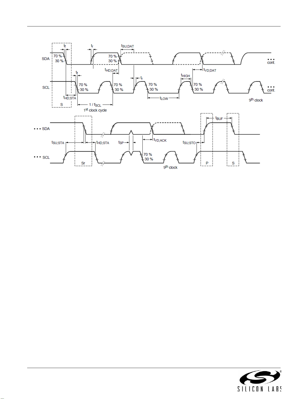
Table 9. I2C Timing Specifications (SCL,SDA)
Parameter Symbol Test Condition Min Max Min Max Units
Standard Mode
100 kbps Fast Mode
400 kbps
SCL Clock
Frequency fSCL 0 100 0 400 kHz
SMBus Timeout — When Timeout is
Enabled 25 35 25 35 ms
Hold time
(repeated) START
condition
tHD:STA 4.0 — 0.6 — µs
Low period of the
SCL clock tLOW 4.7 — 1.3 — µs
HIGH period of
the SCL clock tHIGH 4.0 — 0.6 — µs
Set-up time for a
repeated START
condition
tSU:STA 4.7 — 0.6 — µs
Data hold time tHD:DAT 5.0 — — — µs
Data set-up time tSU:DAT 250 — 100 — ns
Rise time of both
SDA and SCL sig-
nals
tr— 1000 20 300 ns
Fall time of both
SDA and SCL sig-
nals
tf— 300 — 300 ns
Set-up time for
STOP condition tSU:STO 4.0 — 0.6 — µs
Bus free time
between a STOP
and START condi-
tion
tBUF 4.7 — 1.3 — µs
Data valid time tVD:DAT —3.45 — 0.9µs
Data valid
acknowledge time tVD:ACK —3.45 — 0.9µs
Si5341/40
14 Preliminary Rev. 0.9
Figure 2. I2C Serial Port Timing Standard and Fast Modes
Si5341/40
Preliminary Rev. 0.9 15
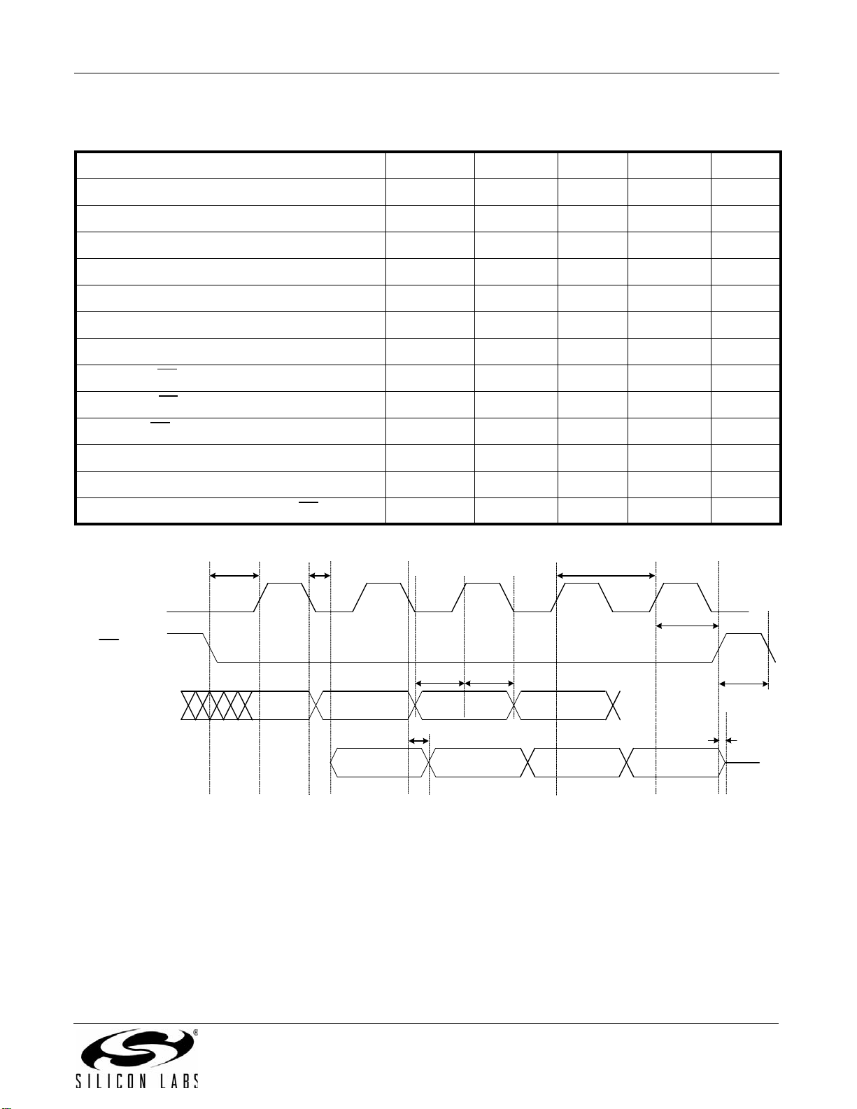
Figure 3. SPI Serial Interface Timing
Table 10. SPI Timing Specifications
(VDD = 1.8 V ±5%, VDDA = 3.3V ±5%, TA=–40to85°C)
Parameter Symbol Min Typ Max Units
SCLK Frequency fSPI ——20MHz
SCLK Duty Cycle TDC 40 — 60 %
SCLK Rise & Fall Time Tr/Tf — — 10 ns
SCLK High & Low Time THL
SCLK Period TC50 — — ns
Delay Time, SCLK Fall to SDO Active TD1 — — 12.5 ns
Delay Time, SCLK Fall to SDO TD2 — — 12.5 ns
Delay Time, CS Rise to SDO Tri-State TD3 — — 12.5 ns
Setup Time, CS to SCLK TSU1 25 — — ns
Hold Time, CS to SCLK Rise TH1 25 — — ns
Setup Time, SDI to SCLK Rise TSU2 12.5 — — ns
Hold Time, SDI to SCLK Rise TH2 12.5 — — ns
Delay Time Between Chip Selects (CS)T
CS 50 — — ns
SCLK
CS
SDI
SDO
TSU1 TD1
TSU2
TD2
TC
TCS
TD3
TH2
TH1
Si5341/40
16 Preliminary Rev. 0.9
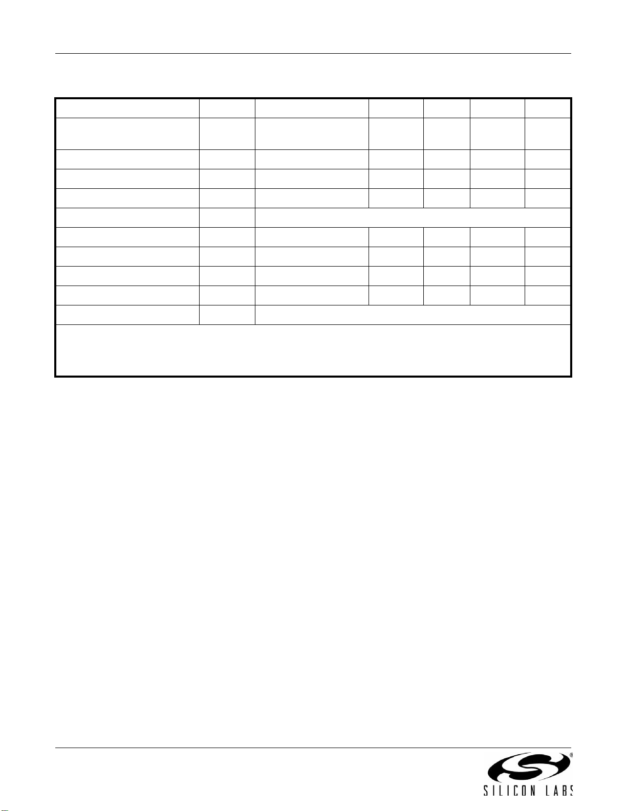
Table 11. Crystal Specifications
Parameter Symbol Test Condition Min Typ Max Units
Crystal Frequency Range fXTAL_48-54 Frequency range for
best jitter performance 48 — 54 MHz
Load Capacitance CL_48-54 —8—pF
Shunt Capacitance CO_48-54 —— 2pF
Crystal Drive Level dL_48-54 ——200µW
Equivalent Series Resistance rESR_48-54 Refer to the Si5341/40 Family Reference Manual to determine ESR.
Crystal Frequency Range fXTAL_25 —25—MHz
Load Capacitance CL_25 —8—pF
Shunt Capacitance CO_25 —— 3pF
Crystal Drive Level dL_25 ——200µW
Equivalent Series Resistance rESR_25 Refer to the Si5341/40 Family Reference Manual to determine ESR
Notes:
1. The Si5341/40 is designed to work with crystals that meet the specifications in Table 11.
2. Refer to the Si5341/40 Family Reference Manual for recommended 48 to 54 MHz crystals. Crystal frequencies from
24.97 to 54.06 MHz are supported, but jitter performance is best from 48 to 54 MHz.
Si5341/40
Preliminary Rev. 0.9 17
Table 12. Thermal Characteristics
Parameter Symbol Test Condition*Value Units
Si5341 - 64QFN
Thermal Resistance
Junction to Ambient JA Still Air 22 °C/W
Air Flow 1 m/s 19.4
Air Flow 2 m/s 18.3
Thermal Resistance
Junction to Case JC 9.5
Thermal Resistance
Junction to Board JB 9.4
JB 9.3
Thermal Resistance
Junction to Top Center JT 0.2
Si5340–44QFN
Thermal Resistance
Junction to Ambient JA Still Air 22.3 °C/W
Air Flow 1 m/s 19.4
Air Flow 2 m/s 18.4
Thermal Resistance
Junction to Case JC 10.9
Thermal Resistance
Junction to Board JB 9.3
JB 9.2
Thermal Resistance
Junction to Top Center JT 0.23
*Note: Based on PCB Dimension: 3” x 4.5”, PCB Thickness: 1.6 mm, PCB Land/Via under GND pad: 36, Number of Cu
Layers: 4

Si5341/40
18 Preliminary Rev. 0.9
Table 13. Absolute Maximum Ratings1,2,3,4
Parameter Symbol Test Condition Value Units
Storage Temperature Range TSTG –55 to +150 °C
DC Supply Voltage VDD –0.5 to 3.8 V
VDDA –0.5 to 3.8 V
VDDO –0.5 to 3.8 V
Input Voltage Range VI1 IN0-IN2, FB_IN -0.85 to 3.8 V
VI2 IN_SEL[1:0],
RST,
OE,
SYNC,
I2C_SEL,
SDI,
SCLK,
A0/CS
A1,
SDA/SDIO
FINC/FDEC
-0.5 to 3.8 V
VI3 XA/XB -0.5 to 2.7 V
Latch-up Tolerance LU JESD78 Compliant
ESD Tolerance HBM 100 pF, 1.5 k2.0 kV
Storage Temperature Range TSTG –55 to 150 °C
Junction Temperature TJCT -55 to 150 °C
Soldering Temperature
(Pb-free profile)5TPEAK 260 °C
Soldering Temperature Time at TPEAK
(Pb-free profile)5TP20-40 sec
Notes:
1. Permanent device damage may occur if the absolute maximum ratings are exceeded. Functional operation should be
restricted to the conditions as specified in the operational sections of this data sheet. Exposure to absolute maximum
rating conditions for extended periods may affect device reliability.
2. 64-QFN and 44-QFN packages are RoHS-6 compliant.
3. For more packaging information, go to www.silabs.com/support/quality/pages/RoHSInformation.aspx.
4. Moisture sensitivity level is MSL2.
5. The device is compliant with JEDEC J-STD-020.

Si5341/40
Preliminary Rev. 0.9 19
3. Detailed Block Diagrams
Figure 4. Si5341 Block Diagram
VDD
VDDA
3
SDA/SDIO
A1/SDO
SCLK
A0/CS
I2C_SEL
SPI/
I2CNVM
RST
Zero Delay
Mode
FB_IN
FB_IN
OE
Si5341
Generator
Clock
÷R0
÷R2
÷R3
÷R4
÷R5
÷R6
÷R7
÷R8
÷R9
÷R1
OUT0
VDDO0
OUT0
OUT2
VDDO2
OUT2
OUT3
VDDO3
OUT3
OUT4
VDDO4
OUT4
OUT5
VDDO5
OUT5
OUT6
VDDO6
OUT6
OUT7
VDDO7
OUT7
OUT8
VDDO8
OUT8
OUT9
VDDO9
OUT9
OUT1
VDDO1
OUT1
÷Pfb
LPF
PD
÷Mn
Md
PLL
IN_SEL[1:0]
XA
XB
25MHz,
48-54MHz
XTAL
Free Run
Mode
Synchronous
Mode
÷P2
÷P1
÷P0
IN0
IN0
IN1
IN1
IN2
IN2
FDEC
FINC
Frequency
Control
÷N0n
N0d t0
÷N2n
N2d
÷N3n
N3d
÷N4n
N4d
t2
t3
t4
÷N1n
N1d t1
MultiSynth
SYNC
Dividers/
Drivers
Status
Monitors
LOL
INTR
OSC
÷PREF
Si5341/40
20 Preliminary Rev. 0.9
Figure 5. Si5340 Detailed Block Diagram
RST
OE
÷Nn0
Nd0 t0
÷N2n
N2d
÷N3n
N3d
t2
t3
÷Nn1
Nd1 t1
LPF
PD
PLL
÷
Mn
Md
LOL
INTR
LOSXAB
SDA/SDIO
A1/SDO
SCLK
A0/CS
I2C_SEL
SPI/
I2CNVM
Status
Monitors
MultiSynth
÷R0
÷R2
÷R3
÷R1
OUT0
VDDO0
OUT0
OUT2
VDDO2
OUT2
OUT3
VDDO3
OUT3
OUT1
VDDO1
OUT1
Dividers/
Drivers
Zero Delay
Mode
FB_IN
FB_IN ÷Pfb
IN_SEL[1:0]
Synchronous
Mode
÷P2
÷P1
÷P0
IN0
IN0
IN1
IN1
IN2
IN2
XA
XB
25MHz,
48-54MHz
XTAL
Free Run
Mode
OSC
÷PREF
Si5340
Generator
Clock
VDD
VDDA
42
This manual suits for next models
1
Table of contents
Other Silicon Laboratories Inverter manuals

Popular Inverter manuals by other brands


Energenie
Energenie EG-PWC-001 user manual

Xantrex
Xantrex XW4024-120/240-60, XW4548-120/240-60,... installation guide

Powtran
Powtran PI9000-S Series user manual

Sunways
Sunways STH-4KTL-HT user manual

NEP
NEP BDG?256 user manual

Generac Power Systems
Generac Power Systems 04673-2 Installation and owner's manual


