SimCom SIM800L Supplement
SIM800L(MT6261)_Hardware Design_V1.01
SIMCOM CONFIDENTIAL FILE

Smart Machine Smart Decision
SIM800L(MT6261)_Hardware Design_V1.012 2016-07-07
Document Title SIM800L(MT6261)_Hardware Design_V1.01
Version 1.01
Date 2016-07-07
Status Release
Document Control ID SIM800L(MT6261)_Hardware Design_V1.01
General Notes
SIMCom offers this information as a service to its customers, to support application and engineering efforts that
use the products designed by SIMCom. The information provided is based upon requirements specifically
provided to SIMCom by the customers. SIMCom has not undertaken any independent search for additional
relevant information, including any information that may be in the customer’s possession. Furthermore, system
validation of this product designed by SIMCom within a larger electronic system remains the responsibility of the
customer or the customer’s system integrator. All specifications supplied herein are subject to change.
Copyright
This document contains proprietary technical information which is the property of SIMCom Limited, copying of
this document and giving it to others and the using or communication of the contents thereof, are forbidden
without express authority. Offenders are liable to the payment of damages. All rights reserved in the event of grant
of a patent or the registration of a utility model or design. All specification supplied herein are subject to change
without notice at any time.
Copyright © Shanghai SIMCom Wireless Solutions Ltd. 2016
SIMCOM CONFIDENTIAL FILE

Smart Machine Smart Decision
SIM800L(MT6261)_Hardware Design_V1.013 2016-07-07
Contents
Table Index................................................................................................................... 6
Figure Index ................................................................................................................. 8
Version History.......................................................................................................... 10
1. Introduction........................................................................................................ 11
2. SIM800L Overview............................................................................................ 11
2.1. SIM800L ............................................................................................................................. 11
2.2. SIM800L Key Features....................................................................................................... 11
2.3. Operating Mode ..................................................................................................................13
2.4. Functional Diagram.............................................................................................................14
3. Package Information ......................................................................................... 15
3.1. Pin Out Diagram .................................................................................................................15
3.2. Pin Description....................................................................................................................15
3.3. Package Dimensions ...........................................................................................................18
4. Application Interface......................................................................................... 20
4.1. Power Supply ......................................................................................................................20
4.1.1. Power Supply Pin................................................................................................................................ 21
4.1.2. Monitoring Power Supply ................................................................................................................... 22
4.2. Power on/off Scenarios .......................................................................................................22
4.2.1. Power on SIM800L............................................................................................................................. 22
4.2.2. Power down SIM800L ........................................................................................................................ 23
4.2.3. Reset Function..................................................................................................................................... 24
4.3. Power Saving Mode ............................................................................................................ 25
4.3.1. Minimum Functionality Mode ............................................................................................................ 26
4.3.2. Sleep Mode 1 (AT+CSCLK=1) .......................................................................................................... 26
4.3.3. Wake Up SIM800L from Sleep Mode 1 ............................................................................................. 26
4.3.4. Sleep Mode 2 (AT+CSCLK=2) .......................................................................................................... 26
4.3.5. Wake Up SIM800L from Sleep Mode 2 ............................................................................................. 27
4.4. RTC Backup........................................................................................................................27
4.5. Serial Port and USB Interface.............................................................................................28
4.5.1 Function of Serial Port ........................................................................................................................ 28
4.5.2 Serial Interfaces................................................................................................................................... 29
4.5.3 Debug Interface................................................................................................................................... 31
4.5.4 Software Upgrade................................................................................................................................ 32
4.6. RI Behaviors .......................................................................................................................32
4.7. Audio Interfaces..................................................................................................................33
SIMCOM CONFIDENTIAL FILE

Smart Machine Smart Decision
SIM800L(MT6261)_Hardware Design_V1.014 2016-07-07
4.7.1. Speaker Interfaces Configuration........................................................................................................ 34
4.7.2. Microphone Interfaces Configuration ................................................................................................. 35
4.7.3. Audio Electronic Characteristic .......................................................................................................... 35
4.7.4. TDD .................................................................................................................................................... 35
4.8. SIM Card Interface..............................................................................................................36
4.8.1. SIM Card Application ......................................................................................................................... 36
4.8.2. SIM Card Design Guide...................................................................................................................... 37
4.8.3. Design Considerations for SIM Card Holder...................................................................................... 37
4.9. PCM Interface .....................................................................................................................39
4.9.1. PCM Interface ..................................................................................................................................... 40
4.10. Keypad Interface .................................................................................................................40
4.11. I2C Bus ...............................................................................................................................42
4.12. General Purpose Input/Output (GPIO) ...............................................................................43
4.13. ADC ....................................................................................................................................43
4.14. PWM ...................................................................................................................................44
4.15. Network Status Indication...................................................................................................45
4.16. Operating Status Indication.................................................................................................45
4.17. LED Interface......................................................................................................................46
4.18. RF Synchronization Signal .................................................................................................46
4.19. Antenna Interface................................................................................................................47
4.19.1. GSM Antenna Interface ................................................................................................................... 47
4.19.2. FM Antenna Interface ...................................................................................................................... 48
5. PCB Layout ........................................................................................................ 50
5.1 Pin Assignment ...................................................................................................................50
5.2 Principle of PCB Layout .....................................................................................................50
5.2.1 Antenna Interface ................................................................................................................................ 51
5.2.2. Power Supply ...................................................................................................................................... 51
5.2.3 SIM Card Interface.............................................................................................................................. 51
5.2.4 Audio Interface.................................................................................................................................... 51
5.2.5 Others .................................................................................................................................................. 51
5.3 Recommended PCB Layout................................................................................................51
6. Electrical, Reliability and Radio Characteristics ........................................... 53
6.1 Absolute Maximum Ratings ...............................................................................................53
6.2 Recommended Operating Conditions .................................................................................53
6.3 Digital Interface Characteristics..........................................................................................53
6.4 SIM Card Interface Characteristics.....................................................................................53
6.5 SIM_VDD Characteristics ..................................................................................................54
6.6 VDD_EXT Characteristics..................................................................................................54
6.7 VRTC Characteristics .........................................................................................................54
6.8 Current Consumption (VBAT=3.8V) .................................................................................54
6.9 Electro-Static Discharge......................................................................................................55
6.10 Radio Characteristics ..........................................................................................................56
6.10.1. Module RF Output Power................................................................................................................ 56
6.10.2. Module RF Receive Sensitivity ....................................................................................................... 57
6.10.3. Module Operating Frequencies........................................................................................................ 57
SIMCOM CONFIDENTIAL FILE

Smart Machine Smart Decision
SIM800L(MT6261)_Hardware Design_V1.015 2016-07-07
7. Manufacturing ................................................................................................... 58
7.1. Top and Bottom View of SIM800L....................................................................................58
7.2. Typical Solder Reflow Profile ............................................................................................58
7.3. The Moisture Sensitivity Level...........................................................................................59
7.4. Baking Requirements..........................................................................................................59
8. Appendix............................................................................................................. 60
I. Related Documents .............................................................................................................60
II. Terms and Abbreviations ....................................................................................................61
III. Safety Caution.....................................................................................................................63
SIMCOM CONFIDENTIAL FILE

Smart Machine Smart Decision
SIM800L(MT6261)_Hardware Design_V1.016 2016-07-07
Table Index
TABLE 1: MODULE INFORMATION ........................................................................................................................... 11
TABLE 2: SIM800L KEY FEATURES............................................................................................................................ 11
TABLE 3: CODING SCHEMES AND MAXIMUM NET DATA RATES OVER AIR INTERFACE ............................ 13
TABLE 4: OVERVIEW OF OPERATING MODES........................................................................................................ 13
TABLE 5: PIN DESCRIPTION ....................................................................................................................................... 15
TABLE 6: RECOMMENDED ZENER DIODE .............................................................................................................. 20
TABLE 7: ELECTRONIC CHARACTERISTIC OF THE RESET PIN.......................................................................... 25
TABLE 8: THE CURRENT CONSUMPTION OF MINIMUM FUNCTIONALITY MODE(AT+CSCLK=1) ............. 26
TABLE 9: SERIAL PORT AND USB PIN DEFINITION ............................................................................................... 28
TABLE 10: SERIAL PORT CHARACTERISTICS......................................................................................................... 28
TABLE 11: VBUS OPERATION VOLTAGE .................................................................................................................. 31
TABLE 12: RI BEHAVIOURS......................................................................................................................................... 32
TABLE 13: AUDIO INTERFACE DEFINITION............................................................................................................ 33
TABLE 14: PERFORMANCE OF AUDIO AMPLIFIER................................................................................................ 34
TABLE 15: MICROPHONE INPUT CHARACTERISTICS........................................................................................... 35
TABLE 16: AUDIO OUTPUT CHARACTERISTICS .................................................................................................... 35
TABLE 17: SIM PIN DEFINITION................................................................................................................................. 36
TABLE 18: PIN DESCRIPTION (MOLEX SIM CARD HOLDER) .............................................................................. 38
TABLE 19: PIN DESCRIPTION (AMPHENOL SIM CARD HOLDER)....................................................................... 39
TABLE 20: PCM PIN DEFINITION ............................................................................................................................... 39
TABLE 21: PCM SPECIFICATION ................................................................................................................................ 40
TABLE 22: PIN DEFINITION OF THE KEYPAD INTERFACE................................................................................... 42
TABLE 23: PIN DEFINITION OF THE I2C ................................................................................................................... 43
TABLE 24: PIN DEFINITION OF THE GPIO................................................................................................................ 43
TABLE 25: PIN DEFINITION OF THE ADC................................................................................................................. 43
TABLE 26: ADC SPECIFICATION ................................................................................................................................ 44
TABLE 27: PIN DEFINITION OF THE PWM ............................................................................................................... 44
TABLE 28: BUZZER CHARACTERISTICS .................................................................................................................. 44
TABLE 29: PIN DEFINITION OF THE NETLIGHT ..................................................................................................... 45
TABLE 30: STATUS OF THE NETLIGHT PIN.............................................................................................................. 45
TABLE 31: PIN DEFINITION OF THE STATUS........................................................................................................... 45
TABLE 32: PIN DEFINITION OF THE LED ................................................................................................................. 46
TABLE 33: ISINK SPECIFICATION .............................................................................................................................. 46
TABLE 34: DEFINITION OF THE RF_SYNC PIN........................................................................................................ 46
TABLE 35: RECOMMENDED TRANSIENT VOLTAGE SUPPRESSOR .................................................................... 48
TABLE 36: ABSOLUTE MAXIMUM RATINGS........................................................................................................... 53
TABLE 37: RECOMMENDED OPERATING CONDITIONS ....................................................................................... 53
TABLE 38: DIGITAL INTERFACE CHARACTERISTICS ........................................................................................... 53
TABLE 39: SIM CARD INTERFACE CHARACTERISTICS........................................................................................ 53
TABLE 40: SIM_VDD CHARACTERISTICS................................................................................................................ 54
TABLE 41: VDD_EXT CHARACTERISTICS ............................................................................................................... 54
TABLE 42: VRTC CHARACTERISTICS ....................................................................................................................... 54
TABLE 43: CURRENT CONSUMPTION ...................................................................................................................... 54
TABLE 44: THE ESD CHARACTERISTICS (TEMPERATURE: 25℃, HUMIDITY: 45 %) ....................................... 55
TABLE 45: GSM850 AND EGSM900 CONDUCTED RF OUTPUT POWER.............................................................. 56
SIMCOM CONFIDENTIAL FILE

Smart Machine Smart Decision
SIM800L(MT6261)_Hardware Design_V1.017 2016-07-07
TABLE 46: DCS1800 AND PCS1900 CONDUCTED RF OUTPUT POWER............................................................... 56
TABLE 47: CONDUCTED RF RECEIVE SENSITIVITY ............................................................................................. 57
TABLE 48: OPERATING FREQUENCIES..................................................................................................................... 57
TABLE 49: MOISTURE SENSITIVITY LEVEL AND FLOOR LIFE ........................................................................... 59
TABLE 50: BAKING REQUIREMENTS ....................................................................................................................... 59
TABLE 51: RELATED DOCUMENTS ........................................................................................................................... 60
TABLE 52: TERMS AND ABBREVIATIONS................................................................................................................ 61
TABLE 53: SAFETY CAUTION..................................................................................................................................... 63
SIMCOM CONFIDENTIAL FILE

Smart Machine Smart Decision
SIM800L(MT6261)_Hardware Design_V1.018 2016-07-07
Figure Index
FIGURE 1: SIM800L FUNCTIONAL DIAGRAM ......................................................................................................... 14
FIGURE 2: PIN ASSIGNMENT (TOP VIEW)................................................................................................................ 15
FIGURE 3: DIMENSIONS OF SIM800L (UNIT: MM).................................................................................................. 18
FIGURE 4: RECOMMENDED PCB FOOTPRINT OUTLINE (UNIT: MM) ................................................................ 19
FIGURE 5: REFERENCE CIRCUIT OF THE VBAT INPUT......................................................................................... 20
FIGURE 6: REFERENCE CIRCUIT OF THE LDO POWER SUPP LY ......................................................................... 20
FIGURE 7: REFERENCE CIRCUIT OF THE DC-DC POWER SUPPLY..................................................................... 21
FIGURE 8: VBAT VOLTAGE DROP DURING TRANSMIT BURST........................................................................... 21
FIGURE 9: THE MINIMAL VBAT VOLTAGE REQUIREMENT AT V B AT DROP .................................................... 22
FIGURE 10: POWERED ON/OFF MODULE USING TRANSISTOR .......................................................................... 22
FIGURE 11: POWERED ON/OFF MODULE USING BUTTON .................................................................................. 22
FIGURE 12: TIMING OF POWER ON MODULE......................................................................................................... 23
FIGURE 13: TIMING OF POWER DOWN SIM800L BY PWRKEY............................................................................ 23
FIGURE 14: TIMING OF RESTART SIM800L.............................................................................................................. 24
FIGURE 15: RESET CIRCUIT........................................................................................................................................ 25
FIGURE 16: RESET TIMING SEQUENCE.................................................................................................................... 25
FIGURE 17: RTC SUPPLY FROM CAPACITOR........................................................................................................... 27
FIGURE 18: RTC SUPPLY FROM NON-CHARGEABLE BATTERY.......................................................................... 27
FIGURE 19: RTC SUPPLY FROM RECHARGEABLE BATTERY .............................................................................. 27
FIGURE 20: CONNECTION OF THE SERIAL INTERFACES..................................................................................... 29
FIGURE 21: RESISTOR MATCHING CIRCUIT ........................................................................................................... 30
FIGURE 22: DIODE ISOLATION CIRCUIT.................................................................................................................. 30
FIGURE 23: TX LEVEL MATCHING CIRCUIT ........................................................................................................... 30
FIGURE 24: RX LEVEL MATCHING CIRCUIT ........................................................................................................... 31
FIGURE 25: USB REFERENCE CIRCUIT .................................................................................................................... 31
FIGURE 26: CONNECTION FOR SOFTWARE UPGRADING AND DEBUGGING .................................................. 32
FIGURE 27: RI BEHAVIOUR OF VOICE CALLING AS A RECEIVER...................................................................... 33
FIGURE 28: RI BEHAVIOUR OF URC OR RECEIVE SMS ........................................................................................ 33
FIGURE 29: RI BEHAVIOUR AS A CALLER ............................................................................................................... 33
FIGURE 30: SPEAKER REFERENCE CIRCUIT .......................................................................................................... 34
FIGURE 31: SPEAKER WITH AMPLIFIER REFERENCE CIRCUIT ......................................................................... 35
FIGURE 32: REFERENCE CIRCUIT OF THE 8-PIN SIM CARD HOLDER............................................................... 36
FIGURE 33: REFERENCE CIRCUIT OF THE 6-PIN SIM CARD HOLDER............................................................... 37
FIGURE 34: MOLEX 91228 SIM CARD HOLDER....................................................................................................... 38
FIGURE 35: AMPHENOL C707 10M006 512 SIM CARD HOLDER........................................................................... 39
FIGURE 36: PCM REFERENCE CIRCUIT.................................................................................................................... 40
FIGURE 37: 25 KEYS REFERENCE CIRCUIT............................................................................................................. 41
FIGURE 38: 50 KEYS REFERENCE CIRCUIT............................................................................................................. 41
FIGURE 39: KEYPAD REFERENCE CIRCUIT ............................................................................................................ 42
FIGURE 40: KEYPAD DETECTED ............................................................................................................................... 42
FIGURE 41: GPIO TIMING SEQUENCES .................................................................................................................... 43
FIGURE 42: REFERENCE CIRCUIT OF PWM DRIVER BUZZER ............................................................................ 44
FIGURE 43: REFERENCE CIRCUIT OF NETLIGHT................................................................................................... 45
FIGURE 44: LED DRIVER REFERENCE CIRCUIT..................................................................................................... 46
FIGURE 45: RF_SYNC SIGNAL DURING TRANSMIT BURST ................................................................................ 47
FIGURE 46: GSM ANTENNA MATCHING CIRCUIT.................................................................................................. 47
SIMCOM CONFIDENTIAL FILE

Smart Machine Smart Decision
SIM800L(MT6261)_Hardware Design_V1.019 2016-07-07
FIGURE 47: GSM SIMPLE ANTENNA MATCHING CIRCUIT .................................................................................. 48
FIGURE 48: FM ANTENNA MATCHING CIRCUIT .................................................................................................... 48
FIGURE 49: GND PIN OF THE EARPHONE USE TO BE THE FM ANTENNA INTERFACE.................................. 49
FIGURE 50: PIN ASSIGNMENT.................................................................................................................................... 50
FIGURE 51: RECOMMENDED PCB LAYOUT ............................................................................................................ 52
FIGURE 52: TOP AND BOTTOM VIEW OF SIM800L................................................................................................. 58
FIGURE 53: TYPICAL SOLDER REFLOW PROFILE OF LEAD-FREE PROCESSES.............................................. 58
SIMCOM CONFIDENTIAL FILE

Smart Machine Smart Decision
SIM800L(MT6261)_Hardware Design_V1.0110 2016-07-07
Version History
Date Version Description of change Author
2016-03-01 1.00 Origin Ajuan.zhu;
Qiang.liu
2016-07-07 1.01 Add note of the over-voltage or under-voltage power down
Add note of the over-temperature or under-
temperature power
down
Add note of the ADC function
Update Figure 47,Figure 48
Add Table 42
Delete the multiplexing function
Update Figure 4
Delete 4.2.2.4 Over-Temperature or Under-
Temperature Power
Down
Ajuan.zhu
SIMCOM CONFIDENTIAL FILE
Smart Machine Smart Decision
SIM800L(MT6261)_Hardware Design_V1.0111 2016-07-07
1. Introduction
This document describes SIM800L hardware interface in great detail. The document can help customer to
quickly understand SIM800L interface specifications, electrical and mechanical details. With the help of this
document and other SIM800L application notes, customer guide, customers can use SIM800L to design various
applications quickly.
2. SIM800L Overview
SIM800L is a quad-band GSM/GPRS module, that works on frequencies GSM850MHz, EGSM900MHz,
DCS1800MHz and PCS1900MHz. SIM800L features GPRS multi-slot class 12/ class 10 (optional) and supports
the GPRS coding schemes CS-1, CS-2, CS-3 and CS-4.
With a tiny configuration of 17.8*15.8*2.4mm, SIM800L can meet almost all the space requirements in
customer applications, such as smart phone, PDA and other mobile devices.
SIM800L is a LGA package with 88 pads, and provides all hardware interfaces between the module and
customer’s boards.
Support 5*5*2 keypads
One full modem serial port, customer can configure two serial ports
One USB, the USB interfaces can debug, download software
Audio channel which includes two microphone input; a receiver output and a speaker output
Programmable general purpose input and output.
A SIM card interface
Support FM
Support one PWM
SIM800L is designed with power saving technique so that the current consumption is as low as 1.11mA in
sleep mode.
2.1. SIM800L
Table 1: Module information
SIM800L
GSM 850,900,1800 and 1900MHz
BT Not support
FLASH 24Mbit
RAM
32Mbit
2.2. SIM800L Key Features
Table 2: SIM800L key features
Feature
Implementation
Power supply
3.4V ~4.4V
Power saving
Typical power consumption in sleep mode is 1.11mA (AT+CFUN=0 )
SIMCOM CONFIDENTIAL FILE
Smart Machine Smart Decision
SIM800L(MT6261)_Hardware Design_V1.0112 2016-07-07
Frequency bands
Quad-band: GSM 850, EGSM 900, DCS 1800, PCS 1900. SIM800L can
search the 4 frequency bands automatically. The frequency bands can also be
set by AT command “AT+CBAND”. For details, please refer to document [1].
Compliant to GSM Phase 2/2+
Transmitting power
Class 4 (2W) at GSM 850 and EGSM 900
Class 1 (1W) at DCS 1800 and PCS 1900
GPRS connectivity
GPRS multi-slot class 12(default)
GPRS multi-slot class 1~12 (option)
Temperature range
Normal operation: -40°C ~ +85°C
Storage temperature -45°C ~ +90°C
Data GPRS
GPRS data downlink transfer: max. 85.6 kbps
GPRS data uplink transfer: max. 85.6 kbps
Coding scheme: CS-1, CS-2, CS-3 and CS-4
PAP protocol for PPP connect
Integrate the TCP/IP protocol.
Support Packet Broadcast Control Channel (PBCCH)
USSD Unstructured Supplementary Services Data (USSD) support
SMS
MT, MO, CB, Text and PDU mode
SMS storage: SIM card
SIM interface
Support SIM card: 1.8V, 3V
External antenna Antenna pad
Audio features
Speech codec modes:
Half Rate (ETS 06.20)
Full Rate (ETS 06.10)
Enhanced Full Rate (ETS 06.50 / 06.60 / 06.80)
Adaptive multi rate (AMR)
Echo Cancellation
Noise Suppression
Serial port and debug
port
Serial port:
Default one Full modem serial port
1200bps to 460800bps.
Can be used for AT commands or data stream.
Support RTS/CTS hardware handshake and software ON/OFF flow control.
Multiplex ability according to GSM 07.10 Multiplexer Protocol.
Autobauding supports baud rate from 1200 bps to 115200bps.
upgrading firmware
Debug port:
USB_DN and USB_DP
Can be used for debugging and upgrading firmware.
Phonebook management
Support phonebook types: SM, FD, LD, RC, ON, MC.
SIM application toolkit GSM 11.14 Release 99
Real time clock Support RTC
Timing functions Use AT command set
Physical characteristics Size: 17.8*15.8*2.4mm
Weight:1.35g
SIMCOM CONFIDENTIAL FILE

Smart Machine Smart Decision
SIM800L(MT6261)_Hardware Design_V1.0113 2016-07-07
Firmware upgrade Main serial port or USB port.(recommend to use USB port)
Table 3: Coding schemes and maximum net data rates over air interface
Coding scheme 1 timeslot 2 timeslot 4 timeslot
CS-1 9.05kbps 18.1kbps 36.2kbps
CS-2 13.4kbps 26.8kbps 53.6kbps
CS-3
15.6kbps
31.2kbps
62.4kbps
CS-4 21.4kbps 42.8kbps 85.6kbps
2.3. Operating Mode
The table below summarizes the various operating modes of SIM800L.
Table 4: Overview of operating modes
Mode
Function
Normal
operation
GSM/GPRS
SLEEP
Module will automatically go into sleep mode
if the conditions of sleep
mode are enabling and there is no
on air and no hardware interrupt (such as
GPIO interrupt or data on serial port).
In this case, the current consumption of module will reduce to the minimal
level.
In sleep mode, the module can still receive paging message and SMS.
GSM
IDLE
Software is active. Module is registered to the GSM network, and the
module is ready to communicate.
GSM
TALK
Connection between two subscribers is in progress. In this case, the power
consumption depends on network settings such as DTX off/on,
FR/EFR/HR, hopping sequences, antenna.
GPRS
STANDBY
Module is ready for GPRS data transfer, but no data is currently sent or
received. In this case, power consumption depends on network settings and
GPRS configuration.
GPRS
DATA
There is GPRS data transfer (PPP or TCP or UDP) in progress. In this case,
power consumption is related with network settings (e.g. power control
level); uplink/downlink data rates and GPRS configuration (e.g. used
multi-slot settings).
Power down
Normal power down by sending AT command “AT+CPOWD=1”
or using the PWRKEY.
The power management unit shuts down the power supply for the baseband part of the
module, and only the power supply for the RTC is remained. Software is not active. The
serial port is not accessible. Power supply (connected to VBAT) remains applied.
Minimum
functionality
mode
AT command “AT+CFUN”
can be used to set the module to a minimum functionality mode
without removing the power supply. In this mode, the RF part of the module will not work
or the SIM card will not be accessible, or both RF part and SIM card will be closed, and the
serial port is still accessible. The power consumption in this mode is lower than normal
mode.
SIMCOM CONFIDENTIAL FILE
Smart Machine Smart Decision
SIM800L(MT6261)_Hardware Design_V1.0114 2016-07-07
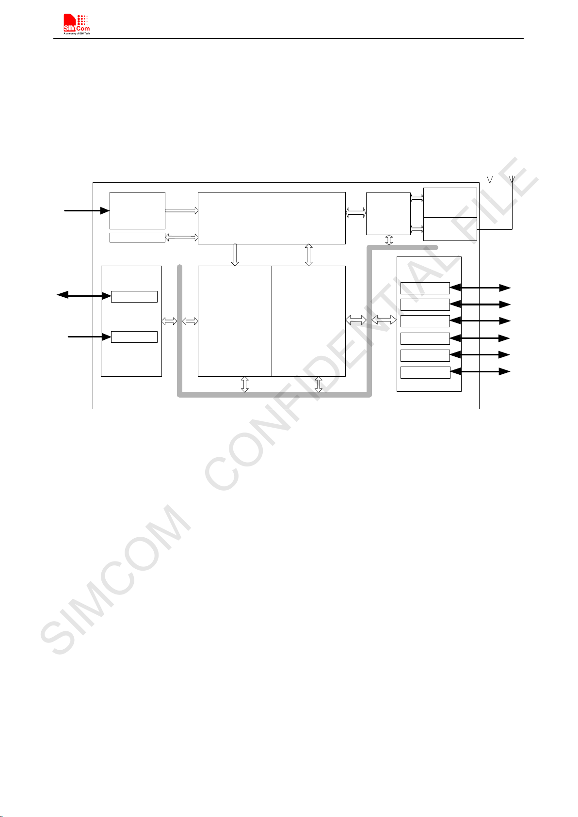
2.4. Functional Diagram
The following figure shows a functional diagram of SIM800L:
GSM baseband
GSM RF
Antenna interface
Other interface
Analog base
band
Digital base
band
Power management unit
Radio
Frequency
Power
Supply
Analog Interface Digital Interface
UART
SIM
GPIOs
RTC
Audio
ADC
RF
FM
USB
KEY
PCM
Figure 1: SIM800L functional diagram
SIMCOM CONFIDENTIAL FILE

Smart Machine Smart Decision
SIM800L(MT6261)_Hardware Design_V1.0115 2016-07-07
3. Package Information
3.1. Pin Out Diagram
GND
VBAT
VBAT
GPIO1
GND
GND
ISINK0
USB_DP
USB_
DP
GND
GND
STA
TUS ISINK1
VBUS
ADC
RESET
GND
PCM_
IN
KBR4
KBR0
KBR1
KBC0
GND
PWM
KBR2
KBC3
VRTC
GSM_
ANT RXD
PWR
KEY
CTS TXDRTS
SCL
SDA DTR
RF_
SYNC
DCD RI
PCM_
SYNC
NETLI
GHT
SPK
1P
MIC
1P
MIC
1N
MIC2P
MIC
2N
GND
SIM_
VDD
SIM_
RST
SPK
1N
SPK
2N
SPK2P
NC
SIM_
CLK
SIM_
DET
SIM_
DATA
VDD_
EXT
GND
86
GND
85
GND
84
GND
GND 87
GND
88
GND
83
GND
GND
80
GND
81
GND
82
GND
1
2
3
4
5
6
7
8
9
10
NC
FM_
ANTP
USB_
DN
GNDGND
GND
GNDGND
GND
GND
GND
78
GND
79
GND
21
3142
43
44
45
46
47
48
49
50
62
61
64
63
66
65
68
67
51 52 53 54 55 56 57 58 59
72 71 70 69
76 75 74 73
60
11 12 13 14 15 16 17 18 19 20
40 39 38 37 36 35 34 33 3241
77
GND
22
30
23
24
25
26
27
28
29
PCM_
CLK
GPIO3
KBC2
KBC4
KBR3
KBC1
PCM_
OUT
GPIO2
Figure 2: Pin assignment (Top view)
3.2. Pin Description
Table 5: Pin description
Pin name Pin number I/O Description Comment
Power supply
VB AT 1,42 I Power supply
VRTC 56 I/O Power supply for RTC It is recommended to
connect with a battery or a
SIMCOM CONFIDENTIAL FILE

Smart Machine Smart Decision
SIM800L(MT6261)_Hardware Design_V1.0116 2016-07-07
capacitor (e.g. 4.7uF).
VDD_EXT 18 O 2.8V power output
If these pins are unused,
keep open.
GND
2,6,8,35,37,38,39,
41,43,44,45,58,67
,71,72,73,76,77,7
8,79,80,81,82,83,
84,85,86,87,88
Ground GND for VBAT recommend
to use 2,43,44,45pin
Power on/down
PWRKEY 48 I
PWRKEY should be pulled low at
least 1 second and then released to
power on/down the module.
Internally pulled up to
V B AT.
Audio interfaces
MIC1P 52 I Differential audio input
If these pins are unused,
keep open.
MIC1N 12
SPK1P 53 O Differential audio output
SPK1N 13
MIC2P 9 I Differential audio input
MIC2N 10
SPK2P 51 O Differential audio output
SPK2N 11
PCM interface
PCM_CLK
29
O
PCM interface for digital audio If these
pins are unused,
keep open.
PCM_OUT 30 O
PCM_SYNC
65
O
PCM_IN 66 I
Keypads interface
KBC4 24 I
Support up to 50 buttons (5*5*2)
If these pins are unused,
keep open.(Please make
sure pin20 at high level
when power on)
KBC3 21 I
KBC2
22
I
KBC1 25 I
KBC0 20 I
KBR4 63 O
KBR3 23 O
KBR2 61 O
KBR1
60
O
KBR0
62
O
GPIO
GPIO1
3
I/O
Programmable general purpose input
and outputGPIO2 27 I/O
GPIO3 28 I/O
SIMCOM CONFIDENTIAL FILE

Smart Machine Smart Decision
SIM800L(MT6261)_Hardware Design_V1.0117 2016-07-07
NETLIGHT 64 O Network status
S TAT U S 4 O Power on status
Serial port
DTR 69 I Data terminal ready
If these pins are unused,
keep open.
RI 68 O Ring indicator
DCD
70
O
Data carrier detect
CTS 34 O Request to send
RTS 33 I Clear to send
TXD 32 O Transmit data
RXD 31 I Receive data
Debug interface
VBUS
7
I
Debug and download
If these pins are unused,
keep open.
USB_DP 59 I/O
USB_DN 19 I/O
ADC
ADC 50 I 10bit
general analog to digital
converter
If these pins are unused,
keep open.
PWM
PWM 26 O Pulse-width modulation
If these pins are unused,
keep open.
I2C
SDA
75
I/O
Open drain output
If these pins are unused,
keep open.
SCL
74
O
Open drain output
SIM card interface
SIM_VDD 16 O
Voltage supply for SIM card.
Support 1.8V or 3V SIM card
All signals of SIM interface
should be protected against
ESD with a TVS diode
array.
SIM _ D ATA
14
I/O
SIM data input/output
SIM_CLK 55 O SIM clock
SIM_RST 15 O SIM reset
SIM_DET 54 I SIM card detection
If these pins are unused,
keep open.
Antenna interface
GSM_ANT
40
I/O
Connect GSM antenna
FM_ANT 17 I Antenna for FM
Synchronizing signal of RF
RF_SYNC 5 O Synchronizing signal of RF
Other
RESET 49 I Reset input(Active low)
ISINK1 46 I Drive keypad backlight
ISINK0 47 I Drive LCD backlight
NC 36、57 - Unconnected KEEP OPEN
SIMCOM CONFIDENTIAL FILE
Smart Machine Smart Decision
SIM800L(MT6261)_Hardware Design_V1.0118 2016-07-07
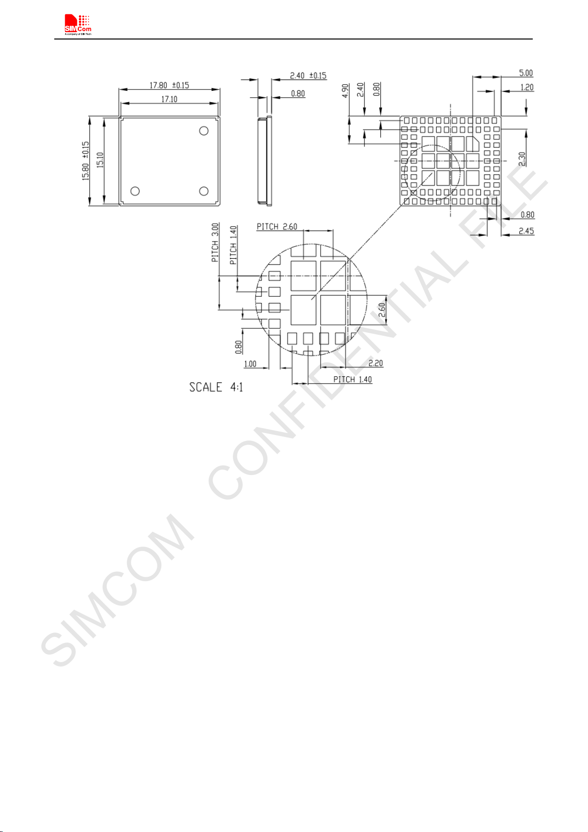
3.3. Package Dimensions
Figure 3: Dimensions of SIM800L (Unit: mm)
SIMCOM CONFIDENTIAL FILE

Smart Machine Smart Decision
SIM800L(MT6261)_Hardware Design_V1.0119 2016-07-07
Figure 4: Recommended PCB footprint outline (Unit: mm)
SIMCOM CONFIDENTIAL FILE
Smart Machine Smart Decision
SIM800L(MT6261)_Hardware Design_V1.0120 2016-07-07
4. Application Interface
4.1. Power Supply
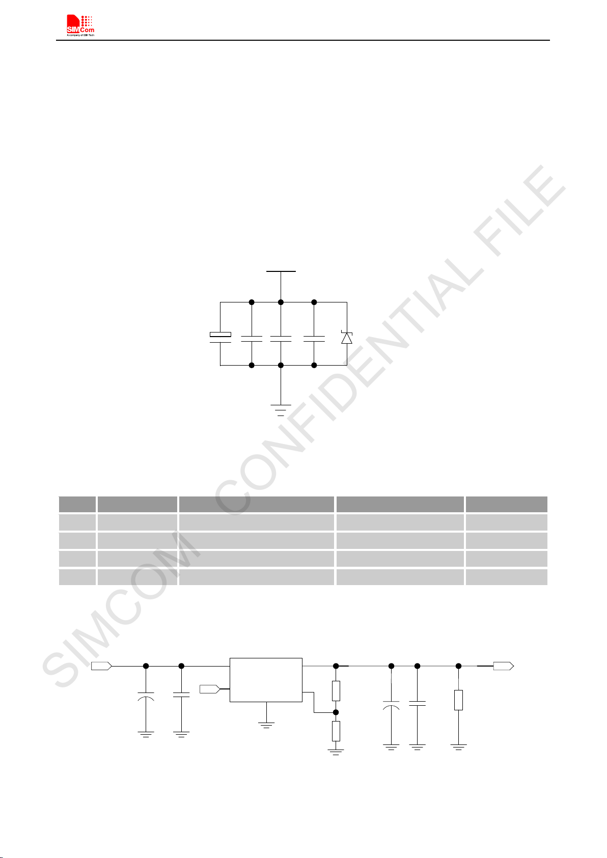
The power supply range of SIM800L is from 3.4V to 4.4V.Recommended voltage is 4.0V.The transmitting burst
will cause voltage drop and the power supply must be able to provide sufficient current up to 2A. For the VBAT
input, a bypass capacitor (low ESR) such as a 100 uF is strongly recommended.
Increase the 33pF and 10pF capacitors can effectively eliminate the high frequency interference. A
5.1V/500mW Zener diode is strongly recommended, the diode can prevent chip from damaging by the voltage
surge. These capacitors and Zener diode should be placed as close as possible to SIM800L VBAT pins.
VBAT
5.1V
500mW
C
A
C
B
33pF 10pF
Figure 5: Reference circuit of the VBAT input
Table 6: Recommended zener diode
Vendor
Part number
Power(watts)
Packages
1
On semi
MMSZ5231BT1G
500mW
SOD123
2 Prisemi PZ3D4V2H 500mW SOD323
3
Vishay
MMSZ4689-V
500mW
SOD123
4 Crownpo CDZ55C5V1SM 500mW 0805
The following figure is the reference design of +5V input power supply. The designed output for the power
supply is 4.1V, thus a linear regulator can be used.
Vin Vout
GND
FB
3
+
PWR_CTRL
R102
R101
VBAT
100K
43K
+C103
330uF
C104
100nF
U101 MIC29302
5
4
1
2
C101 C102
100uF 1uF
DC INPUT
R103
470R
On/Off
Figure 6: Reference circuit of the LDO power supply
SIMCOM CONFIDENTIAL FILE
Table of contents
Other SimCom Recording Equipment manuals


