Skyworks Si5332 User manual

Si5332 Data Sheet
6/8/12-Output Any-Frequency Clock Generator
Based on Skyworks' proprietary MultiSynth™ flexible frequency synthesis technology,
the Si5332 generates any combination of output frequencies with excellent jitter perfor-
mance (190 fs rms). The device's highly flexible architecture enables a single device
to generate a wide range of integer and non-integer related frequencies on up to 12
differential clock outputs with 0 ppm frequency synthesis error. The device offers multi-
ple banks of outputs that can each be tied to independent voltages, enabling usage in
mixed-supply applications. Further, the signal format of each clock output is user-config-
urable. Given its frequency, format, and supply voltage flexibility, the Si5332 is ideally
suited to replace multiple clock ICs and oscillators with a single device.
The Si5332 is quickly and easily configured using ClockBuilder Pro™ software. Clock-
Builder Pro assigns a custom part number for each unique configuration. Devices
ordered with custom part numbers are factory-programmed free of charge, making it
easy to get a custom clock uniquely tailored for each application. Using the Si5332's I2C
interface, the device may be user-configured at power-up or internally-configured NVM
programmed with new configuration using the ClockBuilder Pro Field Programmer.
Applications:
• Servers, Storage, Search Acceleration
•Ethernet Switches, Routers
• Small Cells, Mobile Backhaul/Fronthaul
• Print Imaging
• Communications
•Broadcast Video
• Test and Measurement
• Industrial, Embedded Computing
KEY FEATURES
• Any-Frequency 6/8/12-output
programmable clock generators
•Offered in three different package sizes,
supporting different combinations of output
clocks and user configurable hardware
input pins
• 32-pin, up to 6 outputs
• 40-pin, up to 8 outputs
• 48-pin, up to 12 outputs
• MultiSynth technology enables any-
frequency synthesis on any output up to
250 MHz
• Highly configurable output path featuring a
cross point mux
• Up to three independent fractional
synthesis output paths
• Up to five independent integer dividers
• Embedded 50 MHz crystal option
• Input frequency range:
• External crystal: 16 to 50 MHz
• Differential clock: 10 to 250 MHz
• LVCMOS clock: 10 to 170 MHz
• Output frequency range:
• Differential: 5 to 333.33 MHz
• LVCMOS: 5 to 170 MHz
• User-configurable clock output signal
format per output: LVDS, LVPECL, HCSL,
LVCMOS
• Multi-profile configuration support
• Temperature range: –40 to +85 °C
• Down and center spread spectrum
• RoHS-6 compliant
•Si5332 Family Reference Manual
Skyworks Solutions, Inc. • Phone [781] 376-3000 • Fax [781] 376-3100 • [email protected] • www.skyworksinc.com
1Rev. 1.3 • Skyworks Proprietary Information • Products and Product Information are Subject to Change Without Notice • November 16, 2021 1

Table of Contents
1. Features List ...............................4
2. Ordering Guide ..............................5
3. Functional Description............................6
3.1 Functional Block Diagrams ..........................7
3.2 Modes of Operation ............................9
3.2.1 Initialization .............................9
3.3 Frequency Configuration ..........................9
3.4 Inputs .................................10
3.4.1 External Reference Input (XA/XB) ......................10
3.4.2 Input Clocks .............................10
3.4.3 Input Selection ............................10
3.5 Outputs ................................11
3.5.1 Output Signal Format ..........................11
3.5.2 Differential Output Terminations .......................12
3.5.3 LVCMOS Output Terminations .......................16
3.5.4 LVCMOS Output Signal Swing .......................16
3.5.5 LVCMOS Output Polarity .........................16
3.5.6 Output Enable/Disable ..........................16
3.5.7 Differential Output Configurable Skew Settings..................16
3.5.8 Synchronous Output Disable Feature .....................16
3.6 Spread Spectrum .............................17
3.7 Universal Hardware Input Pins.........................17
3.8 Custom Factory Preprogrammed Parts ......................18
3.9 I2C Serial Interface ............................18
3.10 In-Circuit Programming...........................19
4. Register Map .............................. 20
5. Electrical Specifications .......................... 21
6. Pin Descriptions ............................. 37
6.1 Pin Descriptions (48-Pin) ..........................37
6.2 Pin Descriptions (40-Pin) ..........................42
6.3 Pin Descriptions (32-Pin) ..........................47
7. Package Outline ............................. 51
7.1 Si5332 6x6 mm 48-QFN Package Diagram, External Crystal Versions (Si5332A/B/C/D) .....51
7.2 Si5332 6x6 mm 40-QFN Package Diagram, External Crystal Versions (Si5332A/B/C/D) .....53
7.3 Si5332 5x5 mm 32-QFN Package Diagram, External Crystal Versions (Si5332A/B/C/D) .....54
7.4 Si5332 6x6 mm 48-LGA Package Diagram, Embedded Crystal Versions (Si5332E/F/G/H/L) ....55
7.5 Si5332 6x6 mm 40-LGA Package Diagram, Embedded Crystal Versions (Si5332E/F/G/H/L) ....57
Skyworks Solutions, Inc. • Phone [781] 376-3000 • Fax [781] 376-3100 • [email protected] • www.skyworksinc.com
2Rev. 1.3 • Skyworks Proprietary Information • Products and Product Information are Subject to Change Without Notice • November 16, 2021 2

7.6 Si5332 5x5 mm 32-LGA Package Diagram, Embedded Crystal Versions (Si5332E/F/G/H/L) ....59
8. PCB Land Pattern ............................ 60
8.1 Si5332A/B/C/D 48-QFN Land Pattern ......................60
8.2 Si5332A/B/C/D 40-QFN Land Pattern ......................62
8.3 Si5332A/B/C/D 32-QFN Land Pattern ......................64
8.4 Si5332E/F/G/H/L 48-LGA Land Pattern......................66
8.5 Si5332E/F/G/H/L 40-LGA Land Pattern......................68
8.6 Si5332E/F/G/H/L 32-LGA Land Pattern......................70
9. Top Marking ............................... 72
10. Revision History............................. 73
Skyworks Solutions, Inc. • Phone [781] 376-3000 • Fax [781] 376-3100 • [email protected] • www.skyworksinc.com
3Rev. 1.3 • Skyworks Proprietary Information • Products and Product Information are Subject to Change Without Notice • November 16, 2021 3

1. Features List
• Any-Frequency 6/8/12-output programmable clock generators
• Offered in three different package sizes, supporting different
combinations of output clocks and user configurable hardware
input pins
• 32-pin, up to 6 outputs
• 40-pin, up to 8 outputs
• 48-pin, up to 12 outputs
•MultiSynth™ technology enables any-frequency synthesis on
any output up to 250 MHz
• Integer output frequencies up to 333.33 MHz
• Embedded 50 MHz crystal option (E/F/G/H/L grades)
• Highly configurable output path featuring a cross point mux
• Two independent fractional synthesis output paths
• Up to five independent integer dividers
• Ordering options for embedded 50 MHz reference crystal
• Input frequency range:
• External crystal: 16 to 50 MHz
• Differential clock: 10 to 250 MHz
• LVCMOS clock: 10 to 170 MHz
• Output frequency range:
• Differential: 5 to 333.33 MHz
• LVCMOS: 5 to 170 MHz
• User-configurable clock output signal format per output: LVDS,
LVPECL, HCSL, LVCMOS
• Low phase jitter:
• 175 fs RMS (embedded crystal)
• 190 fs RMS (external crystal)
• PCIe Gen1/2/3/4, SRIS compliant
• 1.8 V, 2.5 V, 3.3 V core VDD
• Adjustable output-output delay
• Multi-profile configuration support:
• Store up to 16 input/output configurations in the same cus-
tom part number
• Independent glitchless on-the-fly output frequency changes
• Very low power consumption
• Independent output supply pins for each bank of outputs:
• 1.8 V, 2.5 V, or 3.3 V differential
• 1.5 V, 1.8 V, 2.5 V, 3.3 V LVCMOS
• Programmable spread spectrum
• Down and center spread from 0.1% to 2.5% in 0.01% steps
at 30 to 33 kHz
• Integrated power supply filtering
•Serial interface: I2C
• ClockBuilder Pro software utility simplifies device configuration
and assigns custom part numbers
• Operating temperature range: –40 to +85 °C
• RoHS-6 compliant
Si5332 Data Sheet • Features List
Skyworks Solutions, Inc. • Phone [781] 376-3000 • Fax [781] 376-3100 • [email protected] • www.skyworksinc.com
4Rev. 1.3 • Skyworks Proprietary Information • Products and Product Information are Subject to Change Without Notice • November 16, 2021 4
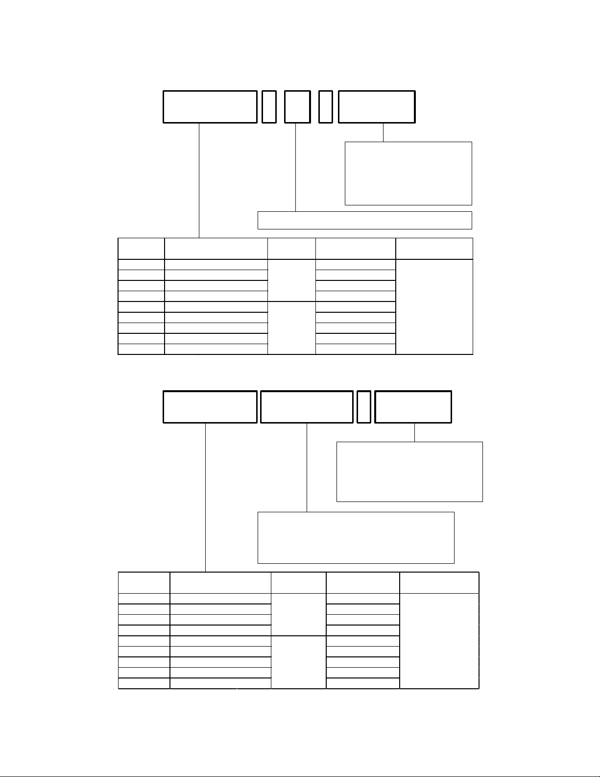
2. Ordering Guide
Si5332X DXXXXX - GMpR
D = Product Revision
XXXXX = NVM code. Aa unique 5-digit ordering sequence
will be assigned by ClockBuilder Pro
Operating Temp Range: -40 to +85 C
GM = ROHS-6 compliant package designator
P = 1 for 6-output, 32-pin QFN/LGA
2 for 8-output, 40-pin QFN/LGA
3 for 12-output, 48-pin QFN/LGA
R = Tape & Reel (ordering option)
D = Product Revision
Operating Temp Range: -40 to +85 C
GM = QFN, ROHS6 compliant
p = 1 for 6-output, 32-pin QFN/LGA
2 for 8-output, 40-pin QFN/LGA
3 for 12-output, 48-pin QFN/LGA
R = Tape & Reel (ordering option)
Preprogrammed Devices Using a ClockBuilder Pro Configuration File
Si5332X - D - GMpR
Blank Devices, In-System Programmable
Ordering Part
Number
Input Type Output Clock
Frequency Range
Operating
Temperature Range
Si5332A 5 MHz - 333.33 MHz
Si5332B 5 MHz - 200 MHz
Si5332C 5 MHz - 333.33 MHz
Si5332D 5 MHz - 200 MHz
Si5332E 5 MHz - 333.33 MHz
Si5332F 5 MHz - 200 MHz
Si5332G 5 MHz - 333.33 MHz
Si5332H 5 MHz - 200 MHz
Si5332L 5 MHz - 333.33 MHz
External
Crystal or
Clock
-40 to +85 °C
Integer and Fractional mode
Integer mode only
Integer mode only
Integer and Fractional mode Embedded
Crystal or
External
Clock
Integer and Fractional mode
Integer mode only
Integer mode only
Integer and Fractional mode
Frequency Synthesis Mode
Integer and Fractional mode
Ordering Part
Number
Input Type Output Clock
Frequency Range
Operating
Temperature Range
Si5332A 5MHz - 333.33MHz
Si5332B 5MHz - 200MHz
Si5332C 5MHz - 333.33MHz
Si5332D 5MHz - 200MHz
Si5332E 5MHz - 333.33MHz
Si5332F 5MHz - 200MHz
Si5332G 5MHz - 333.33MHz
Si5332H 5MHz - 200MHz
Si5332L 5MHz - 333.33MHz
Frequency Synthesis Mode
Integer and Fractional mode
External crystal
or Clock
Integer and Fractional mode
Integer mode only
Integer mode only
Integer and Fractional mode
Embedded
crystal or
External Clock
-40 to +85CInteger and Fractional mode
Integer and Fractional mode
Integer mode only
Integer mode only
Figure 2.1. Orderable Part Number Guide
Si5332 Data Sheet • Ordering Guide
Skyworks Solutions, Inc. • Phone [781] 376-3000 • Fax [781] 376-3100 • [email protected] • www.skyworksinc.com
5Rev. 1.3 • Skyworks Proprietary Information • Products and Product Information are Subject to Change Without Notice • November 16, 2021 5

3. Functional Description
The Si5332 is a high-performance, low-jitter clock generator capable of synthesizing up to twelve user-programmable clock frequencies
up to 333.33 MHz. The device supports free run operation using an external or embedded crystal, or it can lock to an external clock
signal. The output drivers support up to twelve differential clocks or twenty four LVCMOS clocks, or a combination of both. The output
drivers are configurable to support common signal formats, such as LVPECL, LVDS, HCSL, and LVCMOS. VDDO pins are provided
for versatility, which can be set to 3.3 V, 2.5 V, 1.8 V or 1.5 V (CMOS only) to power the multi-format output drivers. The core voltage
supply (VDD) accepts 3.3 V, 2.5 V, or 1.8 V and is independent from the output supplies (VDDOxs). Using its two-stage synthesis
architecture and patented high-resolution low-jitter MultiSynth technology, the Si5332 can generate an entire clock tree from a single
device.
The Si5332 combines a wideband PLL with next generation MultiSynth technology to offer the industry’s highest output count high
performance programmable clock generator, with attainable jitter performance below 200 fs RMS. The PLL locks to either an external
16-50 MHz crystal or an embedded 50 MHz crystal for generating free-running clocks or to an external clock (CLKIN_2/CLKIN_2# or
CLKIN_3/CLKIN_3#) for generating synchronous clocks. In free-run mode, the oscillator frequency is multiplied by the PLL and then
divided down either by an integer divider or MultiSynth for fractional synthesis.
The Si5332 features user-defined universal hardware input pins which can be configured in the ClockBuilder Pro software utility.
Universal hardware pins can be used for OE, spread spectrum enable, input clock selection, output frequency selection, or I2C address
select.
The device provides the option of storing a user-defined clock configuration in its non-volatile memory (NVM), which becomes the
default clock configuration at power-up. To enable in-system programming, a power up mode is available through OTP which powers up
the chip in an OTP defined default mode but with no outputs enabled. This allows a host processor to first write a user defined subset of
the registers and then restart the power-up sequence to activate the newly programmed configuration without re-downloading the OTP.
Si5332 Data Sheet • Functional Description
Skyworks Solutions, Inc. • Phone [781] 376-3000 • Fax [781] 376-3100 • [email protected] • www.skyworksinc.com
6Rev. 1.3 • Skyworks Proprietary Information • Products and Product Information are Subject to Change Without Notice • November 16, 2021 6

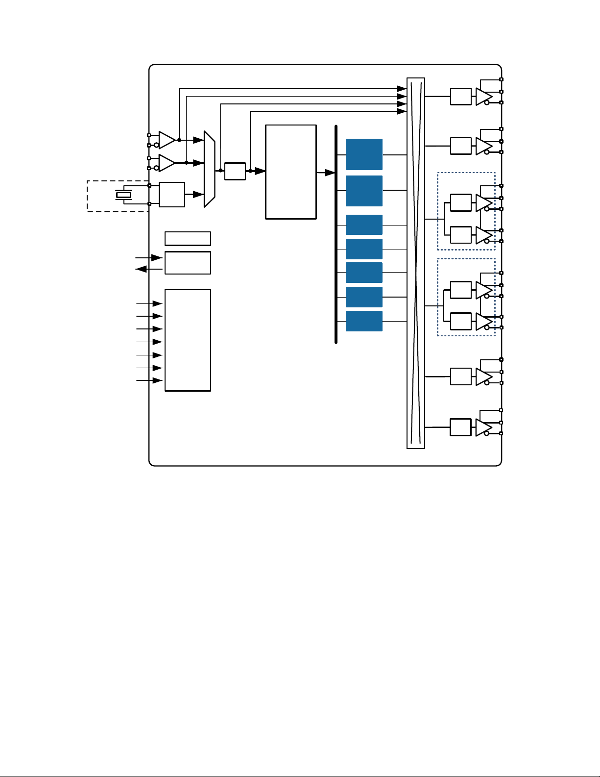
3.1 Functional Block Diagrams
Si5332-GM3: 12-Output, 48-QFN/LGA
Multi
Synth
Multi
Synth
INT
INT
INT
INT
NVM
I2C
SCLK
SDATA
HW Input
Control
Input1
Input2
Input3
Input4
Input5
Input6
Input7
VDDO4
OUT9
OUT9b
÷INT
OUT10
VDDO5
OUT10b
÷INT
OUT11
OUT11b
÷INT
Bank D
OUT0
VDDO0
OUT0b
÷INT
VDDO2
OUT3
OUT3b
÷INT
OUT4
OUT4b
÷INT
OUT5
OUT5b
÷INT
Bank B
OUT1
VDDO1
OUT1b
÷INT
OUT2
OUT2b
÷INT
Bank A
VDDO3
OUT6
OUT6b
÷INT
OUT7
OUT7b
÷INT
OUT8
OUT8b
÷INT
Bank C
XTAL OSC
Si5332A/B/C/D: External Crystal
Si5332E/F/G/H/L: Internal Crystal
PLL
÷INT
CLKIN_3
CLKIN_3b
CLKIN_2
CLKIN_2b
INT
Figure 3.1. Block Diagram for 12-Output Si5332 in 48-QFN/LGA
The Si5332-GM3 features:
• Up to twelve differential clock outputs, with six VDDO pins.
• Seven user-configurable HW input pins, defined using ClockBuilder Pro.
Si5332 Data Sheet • Functional Description
Skyworks Solutions, Inc. • Phone [781] 376-3000 • Fax [781] 376-3100 • [email protected] • www.skyworksinc.com
7Rev. 1.3 • Skyworks Proprietary Information • Products and Product Information are Subject to Change Without Notice • November 16, 2021 7
Si5332-GM2: 8-Output, 40-QFN/LGA
Multi
Synth
INT
Multi
Synth
INT
INT
INT
INT
OUT0
VDDO0
VDDO3
OUT4
OUT1
VDDO1
OUT2
VDDO2
OUT0b
OUT4b
OUT1b
OUT2b
÷INT
÷INT
÷INT
÷INT
NVM
I2C
SCLK
SDATA
PLL
VDDO4
OUT6
OUT6b
÷INT
VDDO5
OUT7
OUT7b
÷INT
OUT3
OUT3b
÷INT
OUT5
OUT5b
÷INT
HW Input
Control
Input1
Input2
Input3
Input4
Input5
Input6
Input7
Bank A
Bank B
CLKIN_3
CLKIN_3b
CLKIN_2
XTAL OSC
CLKIN_2b
Si5332A/B/C/D: External Crystal
Si5332E/F/G/H/L: Internal Crystal
÷INT
Figure 3.2. Block Diagram for 8-Output Si5332 in 40-QFN/LGA
The Si5332-GM2 features:
•Up to eight differential clock outputs, with six VDDO pins.
• Seven user-configurable HW input pins, defined using ClockBuilder Pro.
Si5332 Data Sheet • Functional Description
Skyworks Solutions, Inc. • Phone [781] 376-3000 • Fax [781] 376-3100 • [email protected] • www.skyworksinc.com
8Rev. 1.3 • Skyworks Proprietary Information • Products and Product Information are Subject to Change Without Notice • November 16, 2021 8

Si5332-GM1: 6-Output, 32-QFN/LGA
Multi
Synth
INT
Multi
Synth
INT
INT
INT
INT
OUT0
VDDO0
VDDO3
VDDO4
VDDO5
OUT3
OUT4
OUT5b
OUT1
VDDO1
OUT2
VDDO2
OUT0b
OUT3b
OUT4b
OUT5
OUT1b
OUT2b
÷INT
÷INT
÷INT
÷INT
÷INT
÷INT
NVM
I2C
HW Input
Control
SCLK
SDATA
Input1
Input2
Input3
Input4
Input5
PLL
CLKIN_2
XTAL OSC
CLKIN_2b
Si5332A/B/C/D: External Crystal
Si5332E/F/G/H/L: Internal Crystal
÷INT
Figure 3.3. Block Diagram for 6-Output Si5332 in 32-QFN/LGA
The Si5332-GM1 features:
•Up to six differential clock outputs with individual VDDO.
• Five user-configurable HW input pins, defined using ClockBuilder Pro.
3.2 Modes of Operation
The Si5332 supports both free-run and synchronous modes of operation. The default mode selection is set in ClockBuilder Pro.
Alternatively, two universal hardware input pins can be defined as CLKIN_SEL[1:0] to select between a crystal or clock input. There is
also the option to select the input source via the serial interface by writing to the input select register.
3.2.1 Initialization
Once power is applied, the device begins an initialization period where it downloads default register values and configuration data
from NVM and performs other initialization tasks. Communicating with the device through the serial interface is possible once this
initialization period is complete. The clock outputs will be squelched until the device initialization is done.
3.3 Frequency Configuration
The phase-locked loop is fully integrated and does not require external loop filter components. Its function is to phase lock to the
selected input and provide a common synchronous reference to the high-performance MultiSynth fractional or integer dividers.
A cross point mux connects any of the MultiSynth divided frequencies or INT divided frequencies to individual output drivers or banks
of output drivers. Additional output integer dividers provide further frequency division by an even integer from 1 to 63. The frequency
configuration of the device is programmed by setting the input dividers (P), the PLL feedback fractional divider (Mn/Md), the MultiSynth
fractional dividers (Nn/Nd), and the output integer dividers (R). Skyworks’ Clockbuilder Pro configuration utility determines the optimum
divider values for any desired input and output frequency plan.
Si5332 Data Sheet • Functional Description
Skyworks Solutions, Inc. • Phone [781] 376-3000 • Fax [781] 376-3100 • [email protected] • www.skyworksinc.com
9Rev. 1.3 • Skyworks Proprietary Information • Products and Product Information are Subject to Change Without Notice • November 16, 2021 9

3.4 Inputs
The Si5332 requires an external 16-50 MHz crystal at its XIN/XOUT pins or the embedded 50 MHz crystal to operate in free-run mode,
or an external input clock (CLKIN_2/CLKIN_2# or CLKIN_3/CLKIN_3#) for synchronous operation. An external crystal is not required in
synchronous mode.
3.4.1 External Reference Input (XA/XB)
An external crystal (XTAL) is used in combination with the internal oscillator (OSC) on Si5332A/B/C/D to produce a low jitter reference
for the PLL when operating in the free-run mode. The Si5332 Reference Manual provides additional information on PCB layout
recommendations for the crystal to ensure optimum jitter performance. Refer to Table 5.4 External Crystal Input Specification (A/B/C/D
Grades) on page 24 for crystal specifications.
For free-running operation, the internal oscillator can operate from a low-frequency fundamental mode crystal (XTAL) with a resonant
frequency of 16 to 50 MHz. A crystal can easily be connected to pins XA and XB without external components, as shown in the figure
below. Internal loading capacitance (CL) values from 2.5 pf to 21.5 pf can be selected via register settings. Alternatively, an external CL
can be used along with the internal CL.
Osc To synthesis stage
or output selectors
XTAL
XA
XB
Figure 3.4. External Reference Input (XA/XB)
The Si5332E/F/G/H/L options feature an embedded 50 MHz reference crystal that is used in the free run mode.
3.4.2 Input Clocks
An input clock is available to synchronize the PLL when operating in synchronous mode. This input can be configured as LVPECL,
LVDS or HCSL differential, or LVCMOS. The recommended input termination schemes are shown in the Si5332 Family Reference
Manual. Differential signals must be AC coupled. Unused inputs can be disabled by register configuration.
3.4.3 Input Selection
The active clock input is selected by register control, or by defining two universal input pins as CLKIN_SEL[1:0] in ClockBuilder Pro.
A register bit determines input selection as pin or register selectable. If there is no clock signal on the selected input at power up, the
device will not generate output clocks.
In a typical application, the Si5332 reference input is configured immediately after power-up and initialization. If the device is switched
to another input more than ±1000 ppm offset from the initial input, the device must be recalibrated manually to the new frequency,
temporarily turning off the clock outputs. After the VCO is recalibrated, the device will resume producing clock outputs. If the selected
inputs are within ±1000 ppm, any phase error difference will propagate through the device at a rate determined by the PLL bandwidth.
Hitless switching and phase build-out are not supported by the Si5332.
Si5332 Data Sheet • Functional Description
Skyworks Solutions, Inc. • Phone [781] 376-3000 • Fax [781] 376-3100 • [email protected] • www.skyworksinc.com
10 Rev. 1.3 • Skyworks Proprietary Information • Products and Product Information are Subject to Change Without Notice • November 16, 2021 10

3.5 Outputs
The Si5332 supports up to 12 differential output drivers. Each output can be independently configured as a differential pair or as dual
LVCMOS outputs. The 8-output and 12-output devices feature banks of outputs, with each bank sharing a common VDDO.
Table 3.1. Clock Outputs
Device/Package Maximum Outputs
Si5332-GM1 (32-Pin) 6 Differential, 12 LVCMOS
Si5332-GM2 (40-Pin) 8 Differential, 16 LVCMOS
Si5332-GM3 (48-Pin) 12 Differential, 24 LVCMOS
The output stage is different for each of the three versions of Si5332.
• The 6-output device features individual VDDO pins for each clock output. Each clock output can be sourced from MultiSynth0,
MultiSynth1, the input reference clock, or one of the five INT dividers through the cross point MUX.
• The 8-output device includes four clock outputs with dedicated VDDO pins, each of which can be sourced from MultiSynth0,
MultiSynth1, the input reference clock, or one of the five INT dividers through the cross point MUX. The remaining four clock outputs
are divided into Bank A and Bank B. Each Bank of outputs can be sourced from MultiSynth0, MultiSynth1, the input reference clock,
or one of the five INT dividers through the cross point MUX. The outputs within each of the two Banks share a common VDDO pin.
• The 12-output device includes two clock outputs with dedicated VDDO pins, each of which can be sourced from MultiSynth0,
MultiSynth1, the input reference clock, or one of the five INT dividers through the cross point MUX. The remaining ten clock outputs
are divided into Bank A, Bank B, Bank C, and Bank D. Each Bank of outputs can be sourced from MultiSynth0, MultiSynth1, the
input reference clock, or one of the five INT dividers through the cross point MUX. The outputs within each of the four Banks share a
common VDDO pin.
Utilizing the reference clock enables a fan-out buffer function from an input clock source to any bank of outputs.
Individual output Integer output dividers (R) allow the generation of additional synchronous frequencies. These integer dividers are
configurable as divide by 1 (default) through 63.
3.5.1 Output Signal Format
The differential output swing and common mode voltage are compatible with a wide variety of signal formats including HCSL, LVDS and
LVPECL. In addition to supporting differential signals, any of the outputs can be configured as LVCMOS drivers, enabling the device to
support both differential and single-ended clock outputs. Output formats can be defined in ClockBuilder Pro or via the serial interface.
Si5332 Data Sheet • Functional Description
Skyworks Solutions, Inc. • Phone [781] 376-3000 • Fax [781] 376-3100 • [email protected] • www.skyworksinc.com
11Rev. 1.3 • Skyworks Proprietary Information • Products and Product Information are Subject to Change Without Notice • November 16, 2021 11

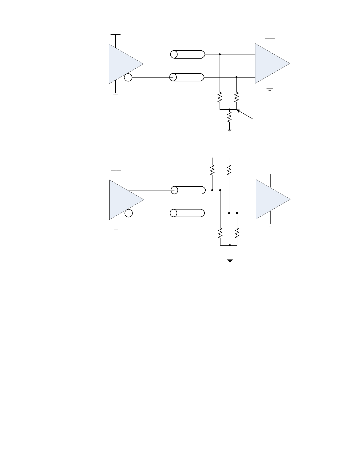
3.5.2 Differential Output Terminations
LVDS Driver Termination
For a general LVDS interface, the recommended value for the differential termination impedance (ZT) is between 90 Ω and 132
Ω. The actual value should be selected to match the differential impedance (Z0) of the transmission line. A typical point-to-point
LVDS design uses a 100 Ω parallel resistor at the receiver and a 100 Ω differential transmission-line environment. In order to avoid
any transmission-line reflection issues, the components should be surface mounted and must be placed as close to the receiver as
possible. The standard LVDS termination schematic as shown in Figure 3.5 Standard LVDS Termination on page 12 can be used with
either type of output structure. Figure 3.6 Optional LVDS Termination on page 12, which can also be used with both output types, is
an optional termination with center tap capacitance to help filter common mode noise. The capacitor value should be approximately
0.01 to 0.1 μF. If using a non-standard termination, please contact Skyworks to confirm if the output structure is current source or
voltage source type. In addition, since these outputs are LVDS compatible, the input receiver’s amplitude and common-mode input
range should be verified for compatibility with the output.
Si5332
LVDS Output
Driver
Zo = ZT/2
+
-
LVDS
Receiver
ZT
Zo = ZT/2
Figure 3.5. Standard LVDS Termination
+
-
LVDS
Receiver
ZT/2
ZT/2
C
Zo = ZT/2
Zo = ZT/2
Si5332
LVDS Output
Driver
Figure 3.6. Optional LVDS Termination
Termination for 3.3 V LVPECL Outputs
The clock layout topology shown below is a typical termination for LVPECL outputs. The two different layouts mentioned are recom-
mended only as guidelines. The differential outputs generate ECL/LVPECL compatible outputs. Therefore, terminating resistors (DC
current path to ground) or current sources must be used for functionality. These outputs are designed to drive 50 Ω transmission
lines. Matched impedance techniques should be used to maximize operating frequency and minimize signal distortion. Figure 3.7 3.3 V
LVPECL Output Termination, Option 1 on page 13 and Figure 3.8 3.3 V LVPECL Output Termination, Option 2 on page 13 show two
different layouts. Other suitable clock layouts may exist, and it would be recommended that the board designers simulate to guarantee
compatibility across all printed circuit and clock component process variations.
Si5332 Data Sheet • Functional Description
Skyworks Solutions, Inc. • Phone [781] 376-3000 • Fax [781] 376-3100 • [email protected] • www.skyworksinc.com
12 Rev. 1.3 • Skyworks Proprietary Information • Products and Product Information are Subject to Change Without Notice • November 16, 2021 12
3.3V 3.3V
LVPECL
Zo=50Ω
Zo=50Ω
R1
50Ω
R2
50Ω
+
-Input
Vcc-2V
RTT
RTT = 54Ω
Si5332
LVPECL Output
Driver
Figure 3.7. 3.3 V LVPECL Output Termination, Option 1
3.3V 3.3V
LVPECL
Zo=50Ω
Zo=50Ω
R1
84Ω
R2
84Ω
+
-Input
R4
125Ω
R3
125Ω
3.3V
Si5332
LVPECL Output
Driver
Figure 3.8. 3.3 V LVPECL Output Termination, Option 2
Si5332 Data Sheet • Functional Description
Skyworks Solutions, Inc. • Phone [781] 376-3000 • Fax [781] 376-3100 • [email protected] • www.skyworksinc.com
13 Rev. 1.3 • Skyworks Proprietary Information • Products and Product Information are Subject to Change Without Notice • November 16, 2021 13

Termination for 2.5 V LVPECL Outputs
Figure 3.9 2.5 V LVPECL Termination Example, Option 1 on page 14 and Figure 3.10 2.5 V LVPECL Termination Example, Option 2
on page 14 show examples of termination for the 2.5 V LVPECL driver option. These terminations are equivalent to terminating 50 Ω
to VDDO – 2 V. For VDDO = 2.5 V, the VDDO – 2 V is very close to ground level. The R3 in Figure 3.10 2.5 V LVPECL Termination
Example, Option 2 on page 14 can be optionally eliminated using the termination shown in Figure 3.9 2.5 V LVPECL Termination
Example, Option 1 on page 14.
2.5V 2.5V
2.5V LVPECL
Driver
Zo=50 Ω
Zo=50 Ω
R1
62.5 Ω
R2
62.5 Ω
+
-Input
R4
250 Ω
R3
250 Ω
2.5V
RTT = 29.5 Ω
Si5332
LVPECL Output
Driver
Figure 3.9. 2.5 V LVPECL Termination Example, Option 1
2.5V 2.5V
2.5V LVPECL
Driver
Zo=50 Ω
Zo=50 Ω
R1
50Ω
R2
50Ω
+
-Input
R3
18Ω
Si5332
LVPECL Output
Driver
Figure 3.10. 2.5 V LVPECL Termination Example, Option 2
Si5332 Data Sheet • Functional Description
Skyworks Solutions, Inc. • Phone [781] 376-3000 • Fax [781] 376-3100 • [email protected] • www.skyworksinc.com
14 Rev. 1.3 • Skyworks Proprietary Information • Products and Product Information are Subject to Change Without Notice • November 16, 2021 14

Termination for HCSL Outputs
The Si5332 HCSL driver option integrated termination resistors to simplify interfacing to an HCSL receiver. The HCSL driver supports
both 100 Ω and 85 Ω transmission line options. This configuration option may be specified using ClockBuilder Pro or via the device I2C
interface.
1.71 V to 3.465 V
OUTx
OUTx
Zo = 42.5 Ω
or 50 Ω
HCSL
Receiver
Zo = 42.5 Ω
or 50 Ω
Si5332
HCSL Output
Driver
Figure 3.11. HCSL Internal Termination Mode
1.71 V to 3.465 V
OUTx
OUTx
Zo = 42.5 Ω
or 50 Ω
HCSL
Receiver
Zo = 42.5 Ω
or 50 Ω
RT = Zo
RT = Zo
Si5332
HCSL Output
Driver
Figure 3.12. HCSL External Termination Mode
Si5332 Data Sheet • Functional Description
Skyworks Solutions, Inc. • Phone [781] 376-3000 • Fax [781] 376-3100 • [email protected] • www.skyworksinc.com
15 Rev. 1.3 • Skyworks Proprietary Information • Products and Product Information are Subject to Change Without Notice • November 16, 2021 15

3.5.3 LVCMOS Output Terminations
LVCMOS outputs can be dc-coupled, as shown in the figure below.
1.71 to 3.465 V
OUTxb
OUTx
Zo=50Ω
Zo=50Ω
Set output driver
to 50Ω mode.
Figure 3.13. LVCMOS Output Termination Example, Option 1
1.425 to 3.465 V
OUTxb
Rs
OUTx Rs
Rs = Zo – Rdrv
(see Table 5.8)
Set output driver
to 25Ω mode.
Figure 3.14. LVCMOS Output Termination Example, Option 2
3.5.4 LVCMOS Output Signal Swing
The signal swing (VOL/VOH) of the LVCMOS output drivers is set by the voltage on the VDDO pin for the respective bank.
3.5.5 LVCMOS Output Polarity
When a driver is configured as an LVCMOS output it generates a clock signal on both pins (OUTx and OUTxb). By default, the
clock on the OUTxb pin is generated in phase with the clock on the OUTx pin. The polarity of these clocks is configurable enabling
complimentary clock generation and/or inverted polarity with respect to other output drivers.
3.5.6 Output Enable/Disable
The universal hardware input pins can be programmed to operate as output enable (OEb), controlling one or more outputs. Pin
assignment is done using ClockBuilder Pro. An output enable pin provides a convenient method of disabling or enabling the output
drivers. When the output enable pin is held high all designated outputs will be disabled. When held low, the designated outputs will be
enabled.
3.5.7 Differential Output Configurable Skew Settings
Skew on the differential outputs can be independently configured. The skew is adjustable in 35 ps steps across a range of 245 ps.
3.5.8 Synchronous Output Disable Feature
Output clocks are always enabled and disabled synchronously. The output will wait until a clock period has completed before the driver
is disabled. This prevents unwanted runt pulses from occurring when disabling an output.
Si5332 Data Sheet • Functional Description
Skyworks Solutions, Inc. • Phone [781] 376-3000 • Fax [781] 376-3100 • [email protected] • www.skyworksinc.com
16 Rev. 1.3 • Skyworks Proprietary Information • Products and Product Information are Subject to Change Without Notice • November 16, 2021 16

3.6 Spread Spectrum
To help reduce electromagnetic interference (EMI), the Si5332 supports spread spectrum modulation. The output clock frequencies can
be modulated to spread energy across a broader range of frequencies, lowering system EMI. The Si5332 implements spread spectrum
using its patented MultiSynth technology to achieve previously unattainable precision in both modulation rate and spreading magnitude.
Spread spectrum can be enabled through I2C, or by configuring one of the universal hardware input pins using ClockBuilder Pro.
The Si5332 features both center and down spread spectrum modulation capability, from 0.1% to 2.5%. Each MultiSynth is capable of
generating an independent spread spectrum clock. The feature is enabled using a user-defined universal hardware input pin or via the
device I2C interface. Spread spectrum can be applied to any output clock derived from a MultiSynth fractional divider, with any clock
frequency up to 250 MHz. Since the spread spectrum clock generation is performed in the MultiSynth fractional dividers, the spread
spectrum waveform is highly consistent across process, voltage and temperature. The Si5332 features two independent MultiSynth
dividers, enabling the device to provide two independent spread profiles simultaneously to the clock output banks.
Spread spectrum is commonly used for 100 MHz PCI Express clock outputs. To comply with the spread spectrum specifications for PCI
Express, the spreading frequency should be set to a maximum of 33 kHz and –0.5% down spread. A universal hardware input pin can
be configured to toggle spread spectrum on/off.
3.7 Universal Hardware Input Pins
Universal hardware input pins are user configurable control input pins that can have one or more of the functions listed below assigned
to them using ClockBuilder Pro.
Universal hardware input pins can be utilized for the following functions:
Table 3.2. Universal Hardware Input Pins
Description Function
SSEN_EN0 Spread spectrum enable on MultiSynth0 (N0).
SSEN_EN1 Spread spectrum enable on MultiSynth0 (N1).
FS_INTx Used to switch an integer output divider frequency from frequency A to frequency B.
FS_MSx Used to switch a MultiSynth output divider output from frequency and/or change spread
spectrum profile.
OE Output enable for one or more outputs.
I2C address select Sets the LSB of the I2C address to either 0 or 1.
CLKIN_SEL[1:0] Selects between crystal or clock inputs.
PROFILE_SEL[x] Selects which device profile to load on power-up. See Multi-Profile description below.
Assigning a universal hardware input pin to control a specific function overrides the register bit control via I2C for that same function.
For example, if a universal hardware pin is assigned as an output enable, it will take precedence over the output enable register bits,
rendering it inoperative.
Spread Spectrum Enable Pins (SSEN[1:0])
Spread_EN[1:0] pins are active pins that enable/disable spread spectrum on all outputs that correspond to MutliSynth0 or MultiSynth1,
respectively. The change in frequency or spread spectrum will be instantaneous and may not be glitch free.
Table 3.3. SSEN_EN Pin Selection Table
SSEN_ENx
0 Spread Spectrum disabled on MultiSynthx
1 Spread Spectrum enabled on MultiSynthx
Si5332 Data Sheet • Functional Description
Skyworks Solutions, Inc. • Phone [781] 376-3000 • Fax [781] 376-3100 • [email protected] • www.skyworksinc.com
17 Rev. 1.3 • Skyworks Proprietary Information • Products and Product Information are Subject to Change Without Notice • November 16, 2021 17

Output Frequency Select Pins
There are five integer dividers, one corresponding to each of the five output banks. Using ClockBuilder Pro, a universal hardware input
pin can be assigned for each integer divider, providing capability to select between two different pre-programmed divide values. Divider
values of every integer from 8 to 255 are available in ClockBuilder Pro for each integer divider.
Table 3.4. FS_INT Pin Selection Table
FS_INTx Output Frequency from INTx
0 Frequency A, as defined in ClockBuilder Pro
1 Frequency B, as defined in ClockBuilder Pro
Output Enable
A universal hardware input pin can be defined to control output enable of a differential output, a bank of differential outputs, or as a
global output enable pin controlling all outputs. Upon de-assertion of an OE pin, the corresponding output will be disabled within 2-6
clock cycles. Asserting an OE pin from disable to enable will take <20 µs for the output to have a clean clock.
Output enabled/disabled for LVCMOS are done in pairs. Each differential buffer True and Compliment output can generate an LVCMOS
clock and the OE pin associated with the True and Compliment output buffer will control the respective LVCMOS pair.
For example: If DIFF0 is configured to be SE1 and DIFF0# is configured to be SE2 and OE1 is the associated OE pin, de-asserting the
OE1 pin will disable both SE1 and SE2 outputs. The disable and enable of the outputs to a known state is glitch free.
I2C Address Pin
This pin sets the LSB of the I2C address. For example, if the I2C address is A6h, setting this pin high will set the I2C address to A7h.
CLKIN_SEL[0:1] Pins
These pins are used to set the input source clock between the input clock channels (Crystal, CLKIN_2/CLKIN_2# or CLKIN_3/
CLKIN_3#). Upon switching the input clock source, the output will not be glitch free. It is intended for the user to set this pin to a known
state before the system is powered up or have the receiver address any unintended output signals when switching to a different input
source clock.
Multi-Profile
Si5332 has the ability to store multiple unique configurations in the same custom part number by enabling multi-profile support in
ClockBuilder Pro after selecting the desired Si5332 device. The ClockBuilder Pro wizard guides users to enter the input/output/feature
set needed for each individual profile configuration, then compiles them together and assigns the necessary number of universal
hardware pins based on the number of profiles entered.
The actual number of profiles supported in a particular design is limited by overall design complexity and NVM size. ClockBuilder Pro
automatically determines the NVM size required for your multi-profile design and will warn if the maximum limit is exceeded.
3.8 Custom Factory Preprogrammed Parts
Custom pre-programmed parts can be ordered corresponding to a specific configuration file generated using the ClockBuilder Pro
software utility. Skyworks writes the configuration file into the device prior to shipping. Use the ClockBuilder Pro custom part number
wizard to quickly and easily generate a custom part number for your ClockBuilder Pro configuration file. A factory pre-programmed part
will generate clocks at power-up.
In less than three minutes, you will be able to generate a custom part number with a detailed data sheet addendum matching your
design’s configuration. Once you receive the confirmation email with the data sheet addendum, simply place an order with your local
Skyworks sales representative. Samples of your pre-programmed device will ship within two weeks.
3.9 I2C Serial Interface
The Si5332 is compatible with rev6 of the I2C specification, including Standard, Fast, and Fast+ modes.
Configuration and operation of the Si5332 can be controlled by reading and writing registers using the I2C . Communication with a 1.8 V
to 3.3 V host is supported. See the Si5332 Family Reference Manual for details.
Si5332 Data Sheet • Functional Description
Skyworks Solutions, Inc. • Phone [781] 376-3000 • Fax [781] 376-3100 • [email protected] • www.skyworksinc.com
18 Rev. 1.3 • Skyworks Proprietary Information • Products and Product Information are Subject to Change Without Notice • November 16, 2021 18

3.10 In-Circuit Programming
The Si5332 is in-system configurable using the I2C interface by the following two methods:
•In-ciruit configuration of device registers after power-up. With this method changes to volatile register memory can be done as re-
quired to produce the desired outputs. This does not alter internal NVM; therefore, register memory changes are lost at power-down.
Refer to the Si5332 Family Reference Manual available on our web site for details.
•In-circuit re-configuration of internal NVM. Writing to internal NVM requires the use of the CBPro Field Programmer (CBPROG-DON-
GLE) and CBPro software. See UG286: ClockBuilderPro Field Programmer Kit user's guide available on our web site for more
information. (One important note: The Si5332 core VDDs (VDD_DIG, VDDA, and VDD_XTAL) must be powered by 3.3 V during
in-circuit NVM programming.)
• VDD core voltages (VDD_DIG, VDDA, VDD_XTAL) must be 3.3 V for in-circuit programming. Using VDD core voltage lower than 3.3
V (i.e., 2.5 V or 1.8 V) will not support reliable in-circuit NVM programming.
Si5332 Data Sheet • Functional Description
Skyworks Solutions, Inc. • Phone [781] 376-3000 • Fax [781] 376-3100 • [email protected] • www.skyworksinc.com
19 Rev. 1.3 • Skyworks Proprietary Information • Products and Product Information are Subject to Change Without Notice • November 16, 2021 19

4. Register Map
Refer to the Si5332 Family Reference Manual for a complete list of registers descriptions and settings.
Si5332 Data Sheet • Register Map
Skyworks Solutions, Inc. • Phone [781] 376-3000 • Fax [781] 376-3100 • [email protected] • www.skyworksinc.com
20 Rev. 1.3 • Skyworks Proprietary Information • Products and Product Information are Subject to Change Without Notice • November 16, 2021 20
This manual suits for next models
8
Table of contents
Other Skyworks Portable Generator manuals


