Slightly Nasty 1411 User manual

M O D E L 1 4 1 1
D U A L D I S C R E T E M I X E R
S L I G H T LY N A S T Y
A
B
M I X
+
A
B
M I X
+
C
L I N
D I S T
C
L I N
D I S T
M O D E L 1 4 1 1
D u a l D i s c r e t e M i x e r
Construction
& Operation Guide
R E V A - F O R P C B V 1 . 0
S L I G H T L Y N A S T Y E L E C T R O N I C S A D E L A I D E , A U S T R A L I A

S L I G H T L Y N A S T Y E L E C T R O N I C S A D E L A I D E , A U S T R A L I A
2
Specifications
S P E C I F I C A T I O N S
PHYSICAL
FORM FACTOR: Loudest Warning / 4U
WIDTH: 3NMW / 75.5mm
HEIGHT: 175mm
DEPTH: ~25mm from panel front inc. components
PCB: 70 x 75mm, Double Sided
CONNECTORS: 4mm Banana
ELECTRICAL
POWER: +12V, 0V, -12V
CONSUMPTION: ~20mA +12V Rail, ~10mA -12V Rail
CONNECTOR: IDC 10-pin Shrouded Header, Eurorack Standard
or MTA-156 4-Pin Header
I/O IMPEDANCES: 100K input, 1K output (nominal)
INPUT RANGES (nominal)
SIGNALS: +/- 5V
OUTPUT RANGES (nominal)
OUTPUT (ALL): +/- 5V
M O D E L 1 4 1 1 D u a l D i s c r e t e M i x e r
IDC power connector pinout.
MTA-156 power connector pinout.

S L I G H T L Y N A S T Y E L E C T R O N I C S A D E L A I D E , A U S T R A L I A
3
Ci rcuit Overv iew
T A B L E O F C O N T E N T S
SPECIFICATIONS
Specifications / Power Requirements 2
INTRODUCTION
Introduction 4
CIRCUIT OVERVIEW
Circuit Overview 5
Input Amplifier 6
Soft Clipping Stage 6
Output Amplifier 8
CHOOSING COMPONENTS
Bill Of Materials (BOM) 9
Choosing Components 10
CONSTRUCTION
Construction Overview 11
Physical Assembly 12
CALIBRATION
Calibrating the 1411 13
CONTROLS
Controls 14
REFERENCE
PCB Guide 15
M O D E L 1 4 1 1 D u a l D i s c r e t e M i x e r
This document is best viewed
in dual-page mode.

S L I G H T L Y N A S T Y E L E C T R O N I C S A D E L A I D E , A U S T R A L I A
4
In troduct ion
I N T R O D U C T I O N
The Slightly Nasty Model 1411 Dual Discrete Mixer is a basic mixer module
that provides two independent 3:1 mixers, with switchable soft-clipping overdrive
distortion and both inverting and non-inverting inputs.
The circuitry in each half of the 1411 is based around a pair of discrete opamp-
type circuits that operate as summing amplifiers - providing signal isolation
between the inputs. Additionally, when in "Linear" mode, input C is inverted,
allowing for more CV mixing and phase cancellation options.
Inputs A and B can also be fine-trimmed to have better unity gain when turned
up to maximum - which is useful when mixing pitch CVs that require accurate
scaling.
The "Distortion" mode engages a soft-clipping diode circuit with an asymmetric
high-frequency response, to emulate the sort of distortions found in some early
synthesiser mixers. This is useful for adding just a touch of saturation and
overdrive to sounds like bass percussion that might otherwise struggle to be
heard in a mix, as well as providing a nice aggression to detuned oscillators.
Because the Model 1411 is a true summing mixer (inputs are added together
rather than averaged), the distortion may be overdriven further by bridging the
inputs together, thus amplifying the input signal by a factor of three, Additionally,
feeding the output back to one of the inputs creates a more aggressive
distortion, going into self-oscillating feedback at higher levels. Experimenting with
different modules in the feedback path opens up a whole world of interesting
distortion timbres and feedback effects.
M O D E L 1 4 1 1
D U A L D I S C R E T E M I X E R
S L I G H T LY N A S T Y
A
B
M I X
+
A
B
M I X
+
C
L I N
D I S T
C
L I N
D I S T
M O D E L 1 4 1 1 D u a l D i s c r e t e M i x e r

S L I G H T L Y N A S T Y E L E C T R O N I C S A D E L A I D E , A U S T R A L I A
5
Ci rcuit Overv iew
C I R C U I T O V E R V I E W
For full schematics, please download the separate schematics PDF. Excerpts shown
in this manual may be outdated and are provided for reference only.
Unsurprisingly for a mixer, the 1411 is an incredibly simple module consisting of
essentially three small elements:
1. Input amplifier - In "Linear" mode this sums together inputs A and B,
while in "Distortion" mode it sums all three inputs.
2. Soft Clipping Stage - This is inserted between the input and output
amplifiers when in "Distortion" mode, and provides a soft-clipping non-
linearity to the signal, with some asymmetry to the high-frequency
response.
3. Output Amplifier - This operates similarly to the input amplifier, but
with an addititional output stage to handle more substantial output
currents. In "Linear" mode this sums the output of the input amplifier
together with input C, while in "Distortion" mode it buffers the output
of the soft-clipping stage.
Block diagram of the Model 1411.
Circles marked "A" are attenuators.
D u a l D i s c r e t e M i x e r
M O D E L 1 4 1 1

W102
BANANA
R123
5K1
1
2
3
RV105
10K
R122
240R
1
2
3
RV106
10K
GND
1
10
234 56 78 9
P101
CONN_02X05
R110
10K
C102
100uF
C101
100uF
C
1
B
2
E
3
Q107
BC560
W101
BANANA
C105
4.7nF
GND
R119
10K
D103
1N4148
D104
1N4148
R105
100K
R111
100K
C103
10pF
R102
10R
VCC
R112
47K R113
12K
R117
2M4
VEE
1
2
3
RV104
100K
D101
1N4148
D102
1N4148
W105
BANANA
W103
BANANA
R101
10R
VEE
VCC
GND
GND
GND
12
3
SW101A
SW_DPDT_x2
45
6SW101B
SW_DPDT_x2
R121
2K2
R118
51K
1
2
3
RV101
100K
GND
GND
C
1
B
2
E
3
Q101
BC550
R107
100K
R106
100K
R104
100K
GND
1
2
3
RV102
100K
R103
100K
VCC
C
1
B
2
E
3
Q108
BC560
R116
10K
C
1
B
2
E
3
Q104
BC550
C
1
B
2
E
3
Q103
BC550
C
1
B
2
E
3
Q102
BC550
R108
51K
R109
10K
C
1
B
2
E
3
Q105
BC560
C
1
B
2
E
3
Q106
BC550
R114
240R
R115
100K
GND
C104
10pF
1
2
3
RV103
100K
GND
R120
100K
VEE
MIX OUT
INPUT A
OFFSET ADJ.
25-turn Lin Trimpot
INPUT B
B GAIN TRIM
INPUT C
A GAIN TRIM
ALL PANEL POTS LINEAR TAPER
S L I G H T L Y N A S T Y E L E C T R O N I C S A D E L A I D E , A U S T R A L I A
6
Ci rcui t O ve rvi ew

S L I G H T L Y N A S T Y E L E C T R O N I C S A D E L A I D E , A U S T R A L I A
7
Ci rcui t O ve rvi ew
The 1411's input amplifier is a classic three-transistor opamp circuit consisting of a
differential pair (Q101 and Q102) that control an output transistor (Q105). The
best way to understand the operation of the differential pair is to consider the
fact that they both share a common emitter resistor (R108) - if one transistor
has a higher voltage at the base, it will conduct more current through this
resistor, raising the voltage across it and consequently reducing the base-emitter
voltage on the other transistor,
As Q102 passes current, it increases the voltage across R109, pulling the base of
Q105 down and turning it on. Because Q105 has no resistor on its emitter to
provide negative feedback, it provides a massive gain boost to the signal,
essentially switching on hard any time a minor current flows through R109/Q102.
What controls this large gain and makes the output voltage across R110 a
meaningful value is the negative feedback path flowing through R105/R123.
As an opamp, the overall circuit around these three transistors can be
understood as a basic inverting summing amplifier as illustrated on the right.
This topology provides isolation between the three inputs by feeding them all
into a "virtual ground" - a common summing node that the opamp automatically
adjusts to be equal to 0v regardless of the currents entering through the input
resistors. Because of this, even though the inputs are all tied to a single point,
there is no way for an individual input signal to bleed into any other as occurs in
purely passive mixing circuits.
Because input C is provided as an inverting input, it bypasses the input amplifier
in LINEAR mode so that it only gœs through a single inverting amplifier stage. In
DISTORTION mode it is rerouted to the front of the input amplifier and becomes
a normal non-inverting input.
The soft-clipping stage is a very simple diode-clipper that takes advantage of the
virtual ground node of the output amplifier to avoid needing to explicitly scale
the signal down and then back up again as is normally required in clipping
circuits. The best way to understand how this works is to imagine that R112 and
R113 are a single normal input resistor feeding an inverting summing amplifier -
we know that at one end will be the input signal, and at the other end will be
the 0V virtual ground - therefore we know that across the length of the resistor
there should be a signal that steadily descreases in amplitude from unity down
to nothing. If we want to gently clip the signal, we need only to "tap off" the
M O D E L 2 2 3 1 A s y m m e t r i c S l e w L i m i t e r
I N P U T A M P L I F I E R
S O F T - C L I P P I N G S T A G E
Typical topology of a summing
amplifier. The negative feedback
through Rf cancels any voltage shift at
the opamp's inverting "-" input and
thus holds it at the same voltage as
the non-inverting "+" input. This
means that each input signal sees only
a resistor connected to 0v, even
though multiple input signals are
connected to the same circuit node.
One way to think of this is that the
signals are each converted into a
current by the input resistors, and the
opamp adjusts the current through Rf
to make it equal to the sum of all the
input currents. As the same current is
flowing both into and out of the node
connected to the opamp's inverting
input, the voltage at that point cannot
change.
D u a l D i s c r e t e M i x e r
M O D E L 1 4 1 1
Voltage response of the soft clip stage
with the input in blue and the output
in red.

resistor at the point where the amplitude is relatively close to the usual diode
drop voltage of ~0.7V. This is done by splitting the one resistor into two, and
ensuring their combined resistance is lower than the summing amp's feedback
resistor in order to supply makeup gain at the output.
the capacitor C105 provides a bypass route for high-frequency signals, and in
practice has the effect of providing a degree of asymmetry to the clipping of
treble content - creating "spikes" on one side of transient content that roughly
emulates the behaviour of certain early synth mixer stages when overdriven. If
desired, this capacitor can be left off for a slightly cleaner overdrive.
The output amplifier operates in essentially exactly the same way as the input
amplifier, but with an additional output stage that can handle the larger and
more variable current draw expected from an output jack. This consists of Q106
and Q108, which are biased by the diodes D103 and D104 to operate as a class-
AB output stage. The emitter resistors R114 and R122 limit the maximum output
current to deal with occasional short circuits etc. that are expected when
making patches in a modular system.
S L I G H T L Y N A S T Y E L E C T R O N I C S A D E L A I D E , A U S T R A L I A
8
Ci rcui t O ve rvi ew
O U T P U T A M P L I F I E R
M O D E L 1 4 1 1 D u a l D i s c r e t e M i x e r

S L I G H T L Y N A S T Y E L E C T R O N I C S A D E L A I D E , A U S T R A L I A
9
Bill Of Materials
B I L L O F M A T E R I A L S
RESISTORS
10R 2 R101, R102
240R 2 R114, R122
2K2 1 R121
5k1 1 R123
10K 4 R109, R110, R116, R119
12K 1 R113
47K 1 R112
51K 2 R108, R118
100K 8 R103, R104, R105, R106, R107, R111, R115, R120
2M4 1 R117
CAPACITORS
10pF 2 C103, C104
4.7nF 1 C105
100uF 2 C101, C102
POTENTIOMETERS
100K 3 RV101, RV102, RV103
1 RV104
2 RV105, RV106
ELECTROMECHANICAL
SW_DPDT 1 SW101
SEMICONDUCTORS
1N4148 4 D101, D102, D103, D104
BC550 5 101, 102, 103, 104, 106
BC560 3 105, 107, 108
CONNECTORS
CONN 2x5pin 1 P101
BANANA 4 W101, W102, W103, W105
( uantities listed are for one PCB)
100K trim
10K trim

S L I G H T L Y N A S T Y E L E C T R O N I C S A D E L A I D E , A U S T R A L I A
10
Ch oos ing Component s
Like all Slightly Nasty modules, the 1411 is designed to use common "jellybean"
components wherever possible, so getting hold of parts is relatively
straightforward. All resistors should be metal film 1% type, and capacitors are
normal electrolytic and film types.
The DPDT On-On switch should be available at most decent suppliers, the main
thing to note is that the top of the switch body (the part that sits against the
front panel, needs to be 10mm from the top of the PCB when the switch is
soldered into place. On some switches (such as those sold at Tayda) this will
mean using a small file to file down the plastic ridge that runs between the
solder terminals.
The trimmers for the gain and offset trimming are standard top-adjust mini
trimpots (sometimes referred to as 6mm trimpots), which use the footprint
shown on the left.
The front panel PCB fits Alpha brand 9mm vertical-mount round shaft
potentiometers, these are widely available from stores such as Thonk, Tayda,
Smallbear, Mouser etc. The module should fit a number of different banana jack
sockets, but the "correct" parts are the Cinch Connectivity range of jacks.
The intended knobs are Davies Molding parts - the 1913BW, 1910CS, and 1900H -
though given the outrageous pricing of the actual Davies 1900H I'd strongly
recommend using a good quality clone. Avoid the cheaper clones without an
internal brass bushing - Thonk sells an excellent brass-bushed 1900H clone for a
very reasonable price that I use in all of my own builds.
Alternatively, feel free to use any knobs that have similar diameters and will fit
the Alpha round shaft pots. The Davies parts are 29mm, 19mm, and 13mm
respectively, and many other manufacturers make knobs of similar sizes. The
classic silver top Moog-style knobs actually work quite well also for the larger
diameters.
C H O O S I N G C O M P O N E N T S
M O D E L 1 4 1 1 D u a l D i s c r e t e M i x e r
The height of the switch body before
installation must be 10mm from the
top of the body to the bottom of the
moulded ridge that runs between the
pins. On some switches this ridge may
need to be filed down slightly with
the edge of a flat needle file or
similar.
The mini trimpots should match the
footprint shown here.

S L I G H T L Y N A S T Y E L E C T R O N I C S A D E L A I D E , A U S T R A L I A
11
Co nst ructio n
C O N S T R U C T I O N
The majority of construction can be performed like any PCB build, starting with
the lowest-profile components (resistors and diodes) and working through to the
taller ones (Capacitors, transistors, etc.). The simplest way to populate the board
is simply to work through the BOM, doing each component type and value in
one chunk before moving on to the next.
When soldering rectangular capacitors, I like to solder one leg on each, then hold
the board in one hand while applying a very light pressure on top of the
capacitor with a free finger, using the other hand to reheat the solder joint until
the capacitor slides down tight against the PCB's surface. Continue this process
for all the installed capacitors then go back and solder the remaining legs. This
approach also works well to mount other components that need to mount
securely onto the board, such as trimpots, IC sockets and pin headers.
When soldering transistors, my preferred approach is to populate the board with
all the transistors of the same type, then solder only the centre leg of each one.
The board can then be flipped over and all the transistors straightened up using
tweezers before soldering the remaining legs. Generally I prefer to only solder
one leg at a time on each transistor to avoid overheating the part, so that they
have time to cool down between soldering operations.
Care must also be taken to ensure that the PCB-mounted potentiometers are
mounted as vertically as possible on the board - one option is to click the
potentiometers into place, then mount them to the front panel before soldering
them. Also note that most potentiometers have a small anti-rotation tab on
them that will need to be removed before soldering them into position, these
can be cut off with a sharp pair of sidecutters, and I personally like to clean up
any remaining protrusions with a few passes of a needle file as well.
The DPDT mode switch in the 1411 is probably the component that requires the
most attention during construction . As mentioned in the "Component Selection"
guide on the previous page, the switch itself must first be checked for correct
height when mounted to the board. Soldering the switch into place should always
be done with the face panel temporarily attached in order to ensure it is vertical,
which means it should be left until after the potentiometers have been soldered
in.
D u a l D i s c r e t e M i x e r
M O D E L 1 4 1 1

Assembling the finished PCBs and front panel is very simple. Begin by fitting the
banana sockets into their respective holes on the front panel - making sure to
align the flat terminals vertically (if using the Cinch-style sockets). The banana
sockets need to be tightened solidly to prevent them coming loose in use,
something like a dab of hot glue between the nut and thread can also help
prevent loosening.
Make sure that the nuts and washers have all been removed from the
potentiometers on the PCB, as well as the anti-rotation tabs on the pots
themselves (if present). Now you can join the front panel and PCB by pushing the
pot shafts through their respective holes, fitting their washers and nuts, and
tightening everything into place.
Now you'll need to connect the banana sockets to the PCB using either some
offcut component leads, or tinned copper wire. The simplest way is to solder the
straight pieces of wire vertically into the pad on the PCB, then bend them over
to meet the banana socket and solder that end to the flat side of the terminal.
This way they can be easily disconnected for servicing by simply heating the
terminal with the iron and pushing the wire away once the solder melts.
P H Y S I C A L A S S E M B L Y
Connecting the banana sockets
using an offcut component lead or
similar.
S L I G H T L Y N A S T Y E L E C T R O N I C S A D E L A I D E , A U S T R A L I A
12
Co nst ructio n
M O D E L 1 4 1 1 D u a l D i s c r e t e M i x e r

C A L I B R A T I O N
Calibration of the 1411 is very simple, and consists of nulling out any small voltage
offset that shows up on the output jack. then setting the correct gain for the A
and B inputs at full scale. Remember to set the mode switch to "LINEAR" before
carrying out these operations.
The discrete amplifier stages in the 1411 will generally show a small output
voltage offset that will need to be nulled out, this is simply accomplished by
setting all the input mix knobs to zero and measuring the voltage between a 0v
point (the screw mounting holes are a good 0v reference point to use) and the
output jack, then adjusting the "OFFSET TRIM" trimmer until you get as close to
0v as possible.
The gain adjustment for the A and B inputs is intended to allow them to be used
as pitch CV inputs in instances where you might want to add pitch modulation
(vibrato from an LFO for example). In this situation you want the input-to-output
gain of that particular signal to be as close to 1:1 as possible, as any scaling of the
signal will result in the loss of the correct 1V/Oct pitch tracking. This requires
manual trimming owing to both the small value variations inherent in the
resistors of the amplifier stages, as well as the considerable variations in
resistance found in different potentiometers.
To set these trimmers, apply a stable voltage of around 5v to the A input (exact
voltage is not important, anywhere between 4-6v will be fine), and then turn the
A mix knob until it is at its maximum setting. Measure the voltage between the
A input jack and the output jack, and adjust the "A GAIN TRIM" trimmer until
you get a reading as close to 0v as possible. Set the mix knob back to zero, and
then repeat the whole process for the B input.
S L I G H T L Y N A S T Y E L E C T R O N I C S A D E L A I D E , A U S T R A L I A
13
Ca librat ion
BEFORE YOU BEGIN
Before powering up the module for the first time, use a multimeter
to check the resistances between the three power rails. Make sure
that they show a resistance higher than 1KOhm, any lower and it's
possible there is a short circuit or incorrectly oriented semiconductor
somewhere on the PCB.
D u a l D i s c r e t e M i x e r
M O D E L 1 4 1 1
M O D E L 1 4 1 1
D U A L D I S C R E T E M I X E R
S L I G H T LY N A S T Y
A
B
M I X
+
A
B
M I X
+
C
L I N
D I S T
C
L I N
D I S T
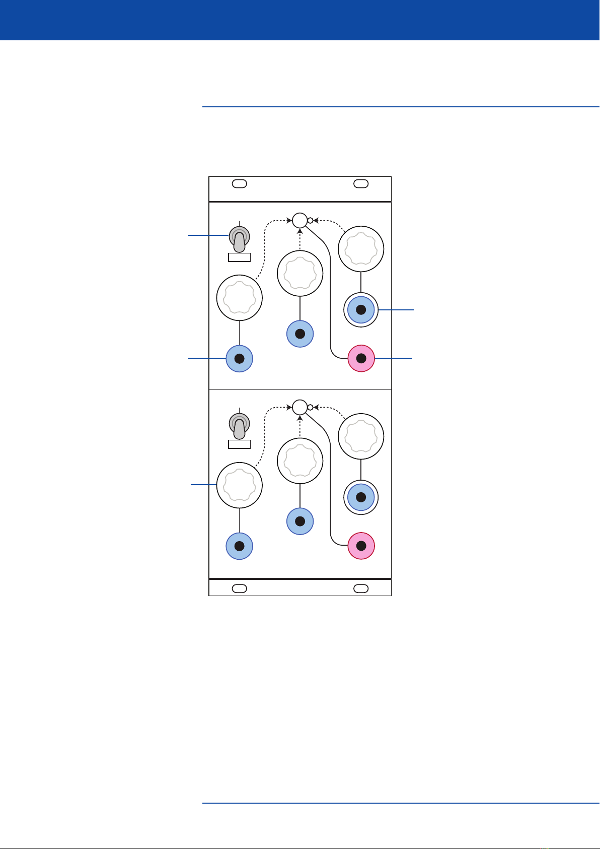
INPUTS
A and B are non-inverting inputs in
both modes.
INPUT C
Inverted input when in LINEAR
mode.
OUTPUT
Outputs the combined input
signals.
MODE SWITCH
Selects between LINEAR and
DISTORTION modes of operation.
INPUT ATTENUATORS
Control how much of the input
signal is sent to the output.
SLIGHTLY NASTY JACK COLOURS
RED Bipolar signal output
BLUE Bipolar signal input
YELLOW AC-coupled input
BLACK Logic output
WHITE Logic Input
C O N T R O L S
S L I G H T L Y N A S T Y E L E C T R O N I C S A D E L A I D E , A U S T R A L I A
14
Co ntrols
M O D E L 1 4 1 1 D u a l D i s c r e t e M i x e r

S L I G H T L Y N A S T Y E L E C T R O N I C S A D E L A I D E , A U S T R A L I A
15
D u a l D i s c r e t e M i x e r
M O D E L 1 4 1 1
PC B Gui de
P C B G U I D E
LOWER BOARD - TOP
LOWER BOARD - BOTTOM

Table of contents


