– 2 –
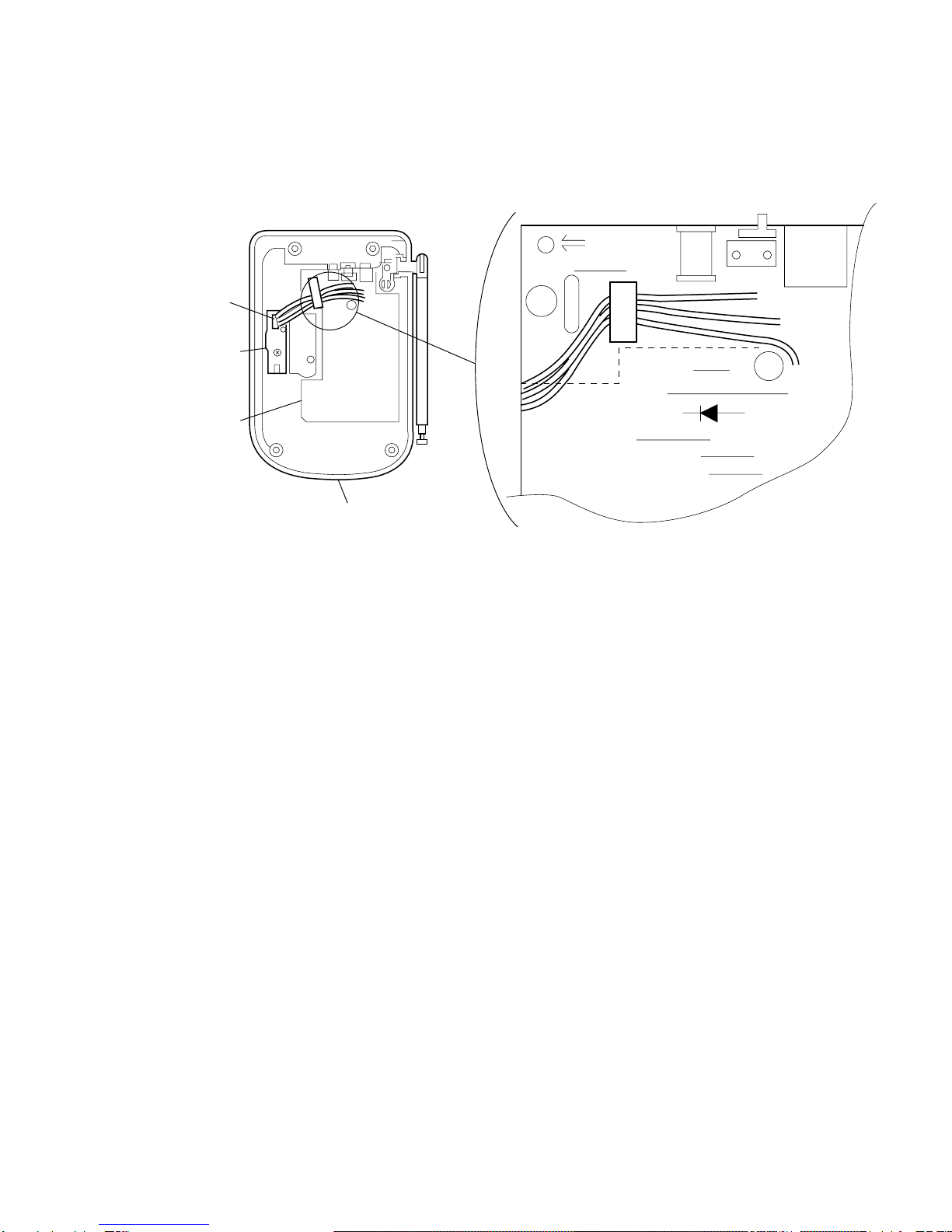
Flexible Circuit Board Repairing
• Keep the temperature of the soldering iron around 270 ˚C dur-
ing repairing.
• Do not touch the soldering iron on the same conductor of the
circuit board (within 3 times).
• Be careful not to apply force on the conductor when soldering
or unsoldering.
Notes on chip component replacement
• Never reuse a disconnected chip component.
• Notice that the minus side of a tantalum capacitor may be dam-
aged by heat.
SAFETY-RELATED COMPONENT WARNING!!
COMPONENTS IDENTIFIED BY MARK !OR DOTTED
LINE WITH MARK !ON THE SCHEMATIC DIAGRAMS
AND IN THE PARTS LIST ARE CRITICAL TO SAFE
OPERATION. REPLACE THESE COMPONENTS WITH
SONY PARTS WHOSE PART NUMBERS APPEAR AS
SHOWN IN THIS MANUAL OR IN SUPPLEMENTS PUB-
LISHED BY SONY.
TABLE OF CONTENTS
1. SERVICING NOTES ................................................ 3
2. GENERAL
Setting up the phone ....................................................... 4
Making and receiving calls ............................................. 4
Speed dialing ................................................................... 5
Resetting the digital security code.................................. 5
Paging .............................................................................. 5
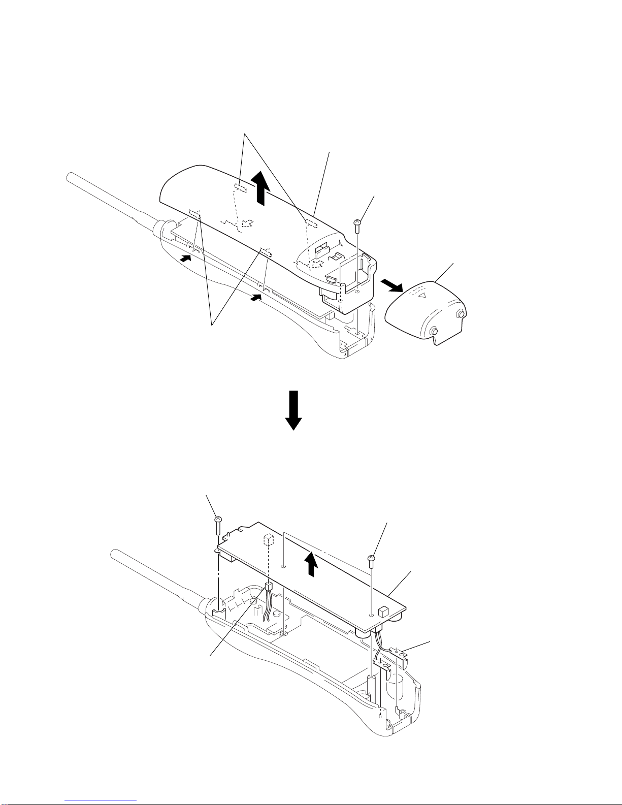
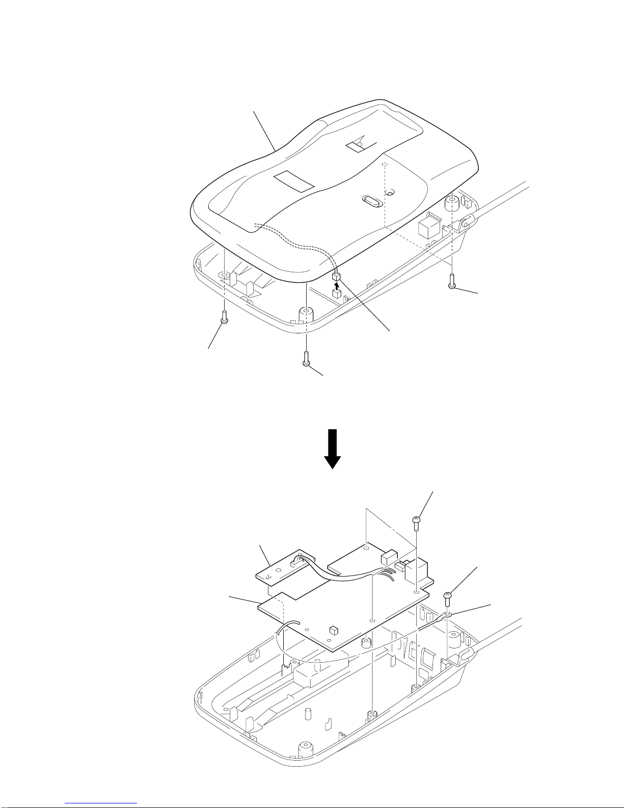
3. DISASSEMBLY ......................................................... 6
4. TEST MODE
4-1. Base Unit Section............................................................ 8
4-2. Handset Section............................................................... 10
5. ELECTRICAL ADJUSTMENTS
5-1. Base Unit Section............................................................ 13
5-2. Handset Section............................................................... 14
6. DIAGRAMS
6-1. Block Diagram – BASE UNIT Section –...................... 19
6-2. Block Diagram – HANDSET Section –........................ 21
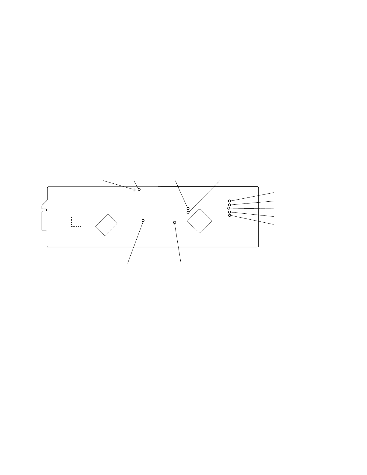
6-3. Notes for Printed Wiring Board and
Schematic Diagram ......................................................... 23
6-4. Printed Wiring Boards – BASE UNIT Section – .......... 25
6-5. Schematic Diagram – BASE UNIT Section –................ 27
6-6. Printed Wiring Board – HANDSET Section –.............. 29
6-7. Schematic Diagram – HANDSET Section –................. 31
6-8. IC Pin Function Description ........................................... 33
7. EXPLODED VIEWS................................................ 35
8. ELECTRICAL PARTS LIST ............................... 37