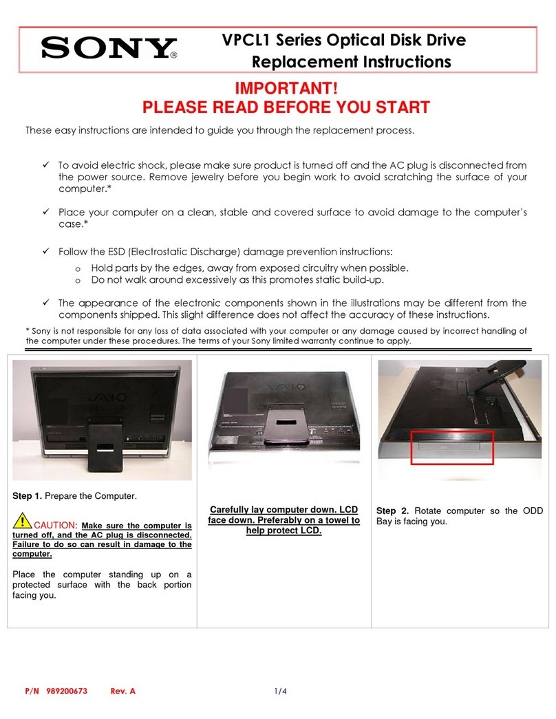
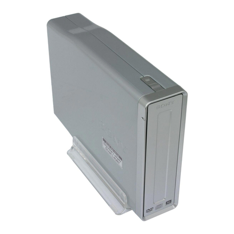
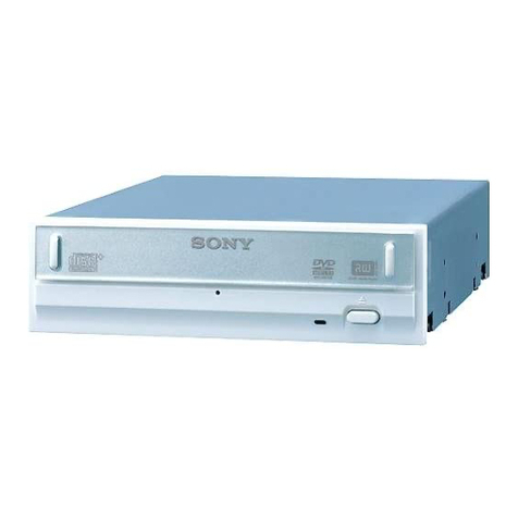
Sony Vaio PCGA-CRWD1 User manual

— 2 —
PCGA-CRWD1 (AM)
Informationinthisdocumentissubjectto change withoutnotice.
Sony andVAIO are trademarks of Sony. Intel logo and Intel Inside
logo are registered trademarks of Intel Corporation. Pentium MMX
is a trademark of Intel Corporation. Microsoft, MS-DOS,Windows,
theWindows 95 and Windows 98 logo are trademarks of Microsoft
Corporation.
All other trademarks are trademarks or registered trademarks of
their respective owners. Other trademarks and trade names may be
used in this document to refer to the entitles claiming the marks and
namesor their produces.Sony Corporationdisclaims any proprietary
interest in trademarks and trade names other than its own.
Service and Inspection Precautions
1. Obey precautionary markings and instructions
Labels and stamps on the cabinet, chassis, and components identify areas
requiring special precautions. Be sure to observe these precautions, as well
as all precautions listed in the operating manual and other associated
documents.
2. Use designated parts only
The set’s components possess important safety characteristics, such as
noncombustibility and the ability to tolerate large voltages. Be sure that
replacement parts possess the same safety characteristics as the originals.
Also remember that the 0mark, which appears in circuit diagrams and
parts lists, denotes components that have particularly important safety
functions; be extra sure to use only the designated components.
3. Alwaysfollowthe originaldesignwhen mounting
parts and routing wires
The original layout includes various safety features, such as inclusion of
insulating materials (tubes and tape) and the mounting of parts above the
printer board. In addition, internal wiring has been routed and clamped so
as to keep it away from hot or high-voltage parts. When mounting parts or
routing wires, therefore, be sure to duplicate the original layout.
4. Inspect after completing service
After servicing, inspect to make sure that all screws, components, and wiring
have been returned to their original condition. Also check the area around
the repair location to ensure that repair work has caused no damage, and
confirm safety.
5. When replacing chip components...
Never reuse components. Also remember that the negative side of tantalum
capacitors is easily damaged by heat.
6. When handling flexible print boards...
•The temperature of the soldering-iron tip should be about 270C.
•Do not apply the tip more than three times to the same pattern.
•Handle patterns with care; never apply force.
Caution: Remember that hard disk drives are easily damaged by
vibration. Always handle with care.
CautionMarkings for Lithium/Ion Battery-The following orsimilar
texts shall be provided on battery pack of equipment or in both the
operating and the service instructions.
CAUTION: Danger of explosion if battery is incorrectly replaced.
Replace only with the same or equivalent type recommended by
the manufacturer. Discard used batteries according to the
manufacturer’s instructions.
CAUTION: The battery pack used in this device may present a fire
or chemical burn hazard if mistreated. Do not disassemble, heat
above 100°C (212°F) or incinerate.
Dispose of used battery promptly.
Keep away from children.
CAUTION: Changing the back up battery.
• Overcharging, short circuiting, reverse charging, multilation or
incineration of the cells must be avoided to prevent one or more of
the following occurrences; release of toxic materials, release of
hydrogen and/or oxygen gas, rise in surface temperature.
• If a cell has leaked or vented, it should be replaced immediately
while avoiding to touch it without any protection.
ATTENTION AU COMPOSANT AYANT RAPPORT
À LA SÉCURITÉ!
LES COMPOSANTS IDENTIFÉS PAR UNE MARQUE 0SUR LES
DIAGRAMMES SCHÉMATIQUES ET LA LISTE DES PIÈCES SONT
CRITIQUES POUR LA SÉCURITÉ DE FONCTIONNEMENT. NE
REMPLACER CES COMPOSANTS QUE PAR DES PIÈSES SONY
DONT LES NUMÉROS SONT DONNÉS DANS CE MANUEL OU
DANS LES SUPPÉMENTS PUBLIÉS PAR SONY.
Confidential

—3 —
TABLE OF CONTENTS
CHAPTER 1. REMOVAL
1-1. Flowchart ......................................................................... 1-1
1-2. Removal ........................................................................... 1-1
1. Cabinet (Lower) ............................................................... 1-1
2. Plate Shield ...................................................................... 1-2
3. IFX-170 Board ................................................................. 1-2
4. IFX-174 Board, Combination Drive, Support PC Board,
Reinforcement, Cabinet (Upper) Assy............................. 1-3
5. Combination Drive, Bezel (Com)Assy ........................... 1-3
(to 1-3)
CHAPTER 2. SELF DIAGNOSTICS ...................... 2-1
(to 2-1)
CHAPTER 3. BLOCK DIAGRAM ·
FRAME HARNESS DIAGRAM ........ 3-1
3-1. Block Diagram ................................................................. 3-1
3-2. Frame Harness Diagram .................................................. 3-2
(to 3-2)
CHAPTER 4. DIAGRAMS ............................................. 4-1
4-1. Semiconductors Index...................................................... 4-1
Semiconductor Pin Assignments ..................................... 4-2
4-2. Schematic Diagrams and Printed Wired Boards Index.... 4-7
1. IFX-170 Board ................................................................. 4-9
2. IFX-174 Board ............................................................... 4-25
(to 4-32)
CHAPTER 5. EXPLODED VIEWS AND
PARTS LIST............................................ 5-1
(to 5-2)
Section Title Page
PCGA-CRWD1 (AM)
Confidential
MEMO

1-1
Confidential
PCGA-CRWD1 (AM)
CHAPTER 1.
REMOVAL
1-1. Flowchart
•P XX means pages that appears in this manual.
1-2. Removal
1. Cabinet (Lower)
POWER
OFF CABINET
(LOWER)
IFX-170
BOARD
P 1-2P 1-1
PLATE
SHIELD
P 1-2
P 1-3
P 1-3
P 1-3
P 1-2
REINFORCEMENT
FLEXIBLE
FLAT
CABLE
COMBINATION
DRIVE
CABINET
(UPPER)
ASSY
P 1-3
P 1-3
SUPPORT
PC BOARD
P 1-3
BEZEL
(COM)
ASSY
IFX-174
BOARD
2Cabinet (Lower)
1Screw (P2X8) (X2) (Black)
Remove the lower cabinet while being
careful not to break the claws (5 claws).

1-2
Confidential
PCGA-CRWD1 (AM)
2. Plate Shield
3. IFX-170 Board
2Screws (P2X2.5) (X2)
(Silver) 3Plate Shield
4Spacer
1Screws (P2X2.5) (X2)
(Silver)
When attaching the spacer, protrude
the spacer exceeding the outer edge
of plate shield by 1mm.
2Screw (P2X2.5) (Silver)
4IFX-170 Board
Flexible Flat Cable
Combination Drive
1Sheet
3
2Screws (P2X2.5) (X2)
(Silver)
When attaching the sheet, align the sheet
with the corner of the combinaton drive.

1-3
Confidential
PCGA-CRWD1 (AM)
(END)
3Screws (P2X2.5) (X2)
(Silver)
1Screws (P2X6) (X2) (Black)
1Screws (P2X6) (Black)
3Screw (P2X2.5)
(Silver)
IFX-174 Board
Flexible Flat Cable
Cabinet (Upper) Assy
Support PC Board
Reinforcement
Combination
Drive
3Screw (P2X2.5)
(Silver)
2
4
6
4
5
COMBO Drive
Bezel (Com) Assy
21Pin, Eject
3Screw (M1.7X3.5) 0 Plate
Special Head (B) (Black)
3Screw (M1.7X3.5)TITE, 0 Plate
Special Head (B) (Black)
4. IFX-174 Board, Combination Drive, Support PC Board, Reinforcement,
Cabinet (Upper) Assy
5. Combination Drive, Bezel (Com) Assy

MEMO

2-1 PCGA-CRWD1 (AM)
Confidential
CHAPTER 2.
SELF DIAGNOSTICS
Please confirm “Self Diagnostics”method which will be informed you with distribution
of “Self Diagnostics”software.
ATTENTION
(END)

MEMO

3-1 PCGA-CRWD1 (AM)
Confidential
CHAPTER 3.
BLOCK DIAGRAM ·FRAME HARNESS DIAGRAM
3-1. Block Diagram
OVP CIRCUIT
Ditect
Ditect
Disable
Close
CD-RW/
DVD-ROM Drive
KME_UJDA710
1394 Bridge
EPSON_SPC7281 1394 PHY
FFM_MD8408B
3.3V Regurator
RICOH_RN5RF33A
3.3V
5.0V
DC-Jack Connector
CN300
1394+POWER Connector
MOLEX_549490-0611
DC/DC Converter
LINEAR_LTC1735
IC300
IC203
IC202IC2001-796-072-21
CN203
Q303
F300

3-2PCGA-CRWD1 (AM)
Confidential
(END)
3-2. Frame Harness Diagram
CN201
10 1
2P i.linkDC INDC IN 10V
Combination
DRIVE
4P
1
CN200
1
50
50
50 2
149
IFX-170 Board
(Side A)
IFX-174 Board
(Side A)
From board to connector (direct connection)
Harness (connector at both end)
Harness (soldered at one end)
Connectors soldered on board and appearing on the panel

4-1
IC
Confidential
PCGA-CRWD1 (AM)
TYPE PAGE
INDEX
CHAPTER 4.
DIAGRAMS
4-1. Semiconductor Index
2SA1314C-TE12L ___________4-6
2SC4783-T1L5/L6 ___________4-6
EC10QS04-TE12L5 __________4-6
EP05Q03L-TE8L3 ___________4-6
HN1K03FU(TR85R) __________4-6
LTC1735CGN#TR ___________4-2
MA8036-TX _________________4-6
MA8056-TX _________________4-6
MA8062-H-TX _______________4-6
MD8408B __________________4-2
RB501V-40TE-17 ____________4-6
RD36SB-T1 _________________4-6
RN5RF33AA-TR _____________4-3
RN5VD16AA-TL _____________4-3
RN5VD42AA-TL _____________4-4
SI4812DY-T1 ________________4-6
SI4894DY-T1 ________________4-6
SML-310MTT86 _____________4-6
SPC7281F0A5 ______________4-4
SSM3KO9FU(T5LSONY1) ____4-6
TC7S14FU(TE85R) __________4-5
TPC8106-H(T2LSONY) _______4-6

4-2
IC
Confidential
PCGA-CRWD1 (AM)
LTC1735CGN#TR (LINEARTECHNOLOGY)
HIGH EFFICIENCY SYNCHRONOUS STEP-DOWN
SWITCHING REGULATOR
–TOP VIEW –
1
2
3
4
5
6
7
8
16
15
14
13
12
11
10
9
C
OSC
RUN/SS
I
TH
FCB
SGND
V
OSENSE
SENSE
–
SENSE
+
TG
BOOST
SW
V
IN
INTV
CC
BG
PGND
EXTV
CC
C
OSC
(Pin 1): External capacitor C
OSC
from this pin to
ground sets the operating frequency.
RUN/SS (Pin 2): Combination of Soft-Start and Run
Control Inputs. A capacitor to ground at this pin sets the
ramp time to full output current. The time is approximately
1.25s/µF. Forcing this pin below 1.5V causes the device to
be shutdown. In shutdown all functions are disabled.
Latchoff overcurrent protection is also invoked via this pin
as described in the Applications Information section.
I
TH
(Pin 3): Error Amplifier Compensation Point. The
current comparator threshold increases with this control
voltage. Nominal voltage range for this pin is 0V to 2.4V.
FCB (Pin 4): Forced Continuous/Synchronization Input.
Tie this pin to ground for continuous synchronous opera-
tion, to a resistive divider from the secondary output when
using a secondary winding or to INTV
CC
to enable Burst
Mode operation at low load currents. Clocking this pin with
a signal above 1.5V
P–P
disables Burst Mode operation but
allows cycle-skipping at low load currents and synchro-
nizes the internal oscillator with the external clock.
SGND (Pin 5): Small-Signal Ground. All small-signal
components such as C
OSC
, C
SS
, the feedback divider plus
the loop compensation resistors and capacitor(s) should
single-point tie to this pin. This pin should, in turn, connect
to PGND.
V
OSENSE
(Pin 6): Receives the feedback voltage from an
external resistive divider across the output.
SENSE
–
(Pin 7): The (–) Input to the Current Comparator.
SENSE
+
(Pin 8): The (+) Input to the Current Comparator.
Built-in offsets between SENSE
–
and SENSE
+
pins in
conjunction with R
SENSE
set the current trip threshold.
EXTV
CC
(Pin 9): Input to the Internal Switch Connected to
INTV
CC
. This switch closes and supplies V
CC
power when-
ever EXTV
CC
is higher than 4.7V. See EXTV
CC
connection
in the Applications Information section. Do not exceed 7V
on this pin and ensure EXTV
CC
≤V
IN
.
PGND (Pin 10): Driver Power Ground. Connects to the
source of bottom N-channel MOSFET, the anode of the
Schottky diode, and the (–) terminal of C
IN
.
BG (Pin 11): High Current Gate Drive for Bottom
N-Channel MOSFET. Voltage swing at this pin is from
ground to INTV
CC
.
INTV
CC
(Pin 12): Output of the Internal 5.2V Regulator and
EXTV
CC
Switch. The driver and control circuits are pow-
ered from this voltage. Decouple to power ground with a
1µF ceramic capacitor placed directly adjacent to the IC
together with a minimum of 4.7µF tantalum or other low
ESR capacitor.
V
IN
(Pin 13): Main Supply Pin. Must be closely decoupled
to power ground.
SW (Pin 14): Switch Node Connection to Inductor and
Bootstrap Capacitor. Voltage swing at this pin is from a
Schottky diode (external) voltage drop below ground to
V
IN
.
BOOST (Pin 15): Supply to Topside Floating Driver. The
bootstrap capacitor is returned to this pin. Voltage swing
at this pin is from a diode drop below INTV
CC
to (V
IN
+
INTV
CC
).
TG (Pin 16): High Current Gate Drive for Top N-Channel
MOSFET. This is the output of a floating driver with a
voltage swing equal to INTV
CC
superimposed on the
switch node voltage SW.
PIN FUNCTIONS
FUNCTIONAL DIAGRAM
SW
–
+
+
–
0.86V
–
+
0.55V
2.4V
0.8V 0.86V
I
1
+
–I
2
+
–EA
A
BURST
DISABLE
FC
OV
gm =1.3mΩ
B
–
+
4.7V
IREV
+
–
+
–F
FC
S
R
Q
DROP
OUT
DET
0.8V
REF
SWITCH
LOGIC
SD
6V
R1
RUN/SS
C
SS
R
C
V
OSENSE
V
FB
1.2∝ARUN
SOFT-
START
+
OVER-
CURRENT
LATCHOFF
SD
I
TH
C
C
0.17∝A
OSC
4(V
FB
)BUFFERED
I
TH
SLOPE COMP
+– –+
3mV
ICMP
R2
2k 45k
BOT
TOP ON
FORCE BOT
45k
30k 30k
SENSE
+
SENSE
–
SYNC
1.2V 0.8V
C
TOP
UVL
BOT
INTV
CC
5.2V
LDO
REG
V
IN
+
C
INTVCC
V
OUT
V
SEC
INTV
CC
BG
PGND
V
IN
V
IN
BOOST
TG
INTV
CC
C
B
D
B
D
1
C
OSC
+
C
IN
+
C
SEC
+
C
OUT
EXTV
CC
FCBSGNDC
OSC
R
SENSE
1 5 4
13
15
16
14
12
11
10
9783
2
6
MD8408B (FUJIFILM MICRODEVICES)
IEEE 1394 PHYSICAL LAYER IC
–TOP VIEW –

4-3
IC
Confidential
PCGA-CRWD1 (AM)
RN5RF33AA-TR (RICOH)
LOW RIPPLE REGULATOR WITHTRANSISTOR CONNECTED
EXTERNALLY
–TOP VIEW –
RN5VD16AA-TL (RICOH)
CMOS VOLTAGE DETECTOR
–TOP VIEW –

4-4
IC
Confidential
PCGA-CRWD1 (AM)
RN5VD42AA-TL (RICOH)
CMOS VOLTAGE DETECTOR
–TOP VIEW –
Pin No. Symbol Description
1OUT Output Pin
Input and power source for device itself
Ground Pin
No Connection
Pin for external capacitor (for setting output delay)
2 VDD
3GND
4NC
5 CD
SPC7281F0A5 (EPSON)
IEEE1394 CONTROLLER
–TOP VIEW –
VSS
N.C.
P21
P20
XCE10EX
XCE9
MonxWait
XCE6
HVDD
TO0
TO1
TO2
TO3
TO4
TO5
TO6
TO7
TI8
MonxInt
VSS
VSS
VSS
VSS
LREQ
LVDD
SCLK
VSS
CNA
XISO
BHEN
CTL0
CTL1
D0
D1
D2
LVDD
D3
D4
D5
D6
D7
PD
LPS
LINKON
N.C
LVDD
138 137 136 135 134 133 132 131 130 129 128 127 126 125 124 123 122 121 120 119 118 117 116 115 114 113 112 111 110 109 108 107 106 105 104 103 102 101 100 99 98 97 96 95 94 93
LVDD
139 92
VSS
N.C
140 91
N.C.
P22
141 90
XHRST
P23
142 89
HDD7
K66
143 88
HDD8
K67
144 87
HDD6
XWAIT
145 86
HDD9
P00
146 85
HDD5
P01
147 84
HDD10
VSS
148 83
HVDD
P02
149 82
HDD4
P03
150 81
HDD11
P04
151 80
HDD3
P05
152 79
HDD12
P06
153 78
HDD2
P07
154 77
HDD13
X2SPDX
155 76
HDD1
RAMTST
156 75
VSS
VSS
157 74
HDD14
PLLC
158 73
HDD0
VSS
159 72
HDD15
PLLS0
160 71
HDMARQ
PLLS1
161 70
XHIOW
EA10MD0
162 69
XHIOR
EA10MD1
163 68
HIORDY
EA10MD2
164 67
HVDD
HVDD
165 66
XHDMACK
P14
166 65
HINTRQ
P13
167 64
HDA1
P12
168 63
XHPDIAG
P11
169 62
HDA0
VSS
170 61
HDA2
OSC3
171 60
XHCS0
OSC4
172 59
XHCS1
VSS
173 58
TVEP
P10
174 57
VSS
DSIO
175 56
XHDASP
HVDD
176 55
FLSTST
XNMI
177 54
AD23
XRESET178 53
AD22
ICEMD179 52
AD21
VSS
180 51
AD20
HCLK
181 50
AD19
BCLK
182 49
AD18
N.C.
183 48
N.C.
VSS
184 47
LVDD
1 2 3 4 5 6 7 8 9 10111213 141516171819202122232425262728293031323334353637383940414243444546
LVDD
N.C
DT0
DT1
HVDD
DT2
DT3
DT4
DT5
DT6
DT7
DT8
VSS
DT9
DT10
DT11
DT12
DT13
DT14
DT15
HVDD
XWRH
XWRL
XRD
AD0
AD1
AD2
AD3
VSS
AD4
AD5
AD6
AD7
AD8
AD9
AD10
HVDD
AD11
AD12
AD13
AD14
AD15
AD16
AD17
N.C.
VSS
EPSON
SPC7281F0A
Top View
INDEX
1394
PHY/LINK I/F
1394
LINK & TRAN
Core
Register for
LINK&TRAN
AsyncTx
FIFO
IsoTx
FIFO
Rx
FIFO
DMA
for ATF
DMA
for ITF
DMA
for RF
Register
for 1394Tx/Rx
Buffer I/F Maneger
TRAN & SBP2
Control
Register
for TRAN&SBP2
IDE
FIFO
IDE
DMA
Register
for IDE
IDE
I/F
Internal Packet Memory(8KByte)
Rx
FIFO
C33 Core Block
C33_PERI
(Prescaaler,8-bit timer,16bit timer,Clock timer,
serial interface,Ports)
PERI
PAD
C33 peripheral Block
C33__CORE
(CPU,BCU,ITC,CLG,DBG)
C33_SBUS
CORE
PAD
Internal
RAM
(8KByte)
C33 Internal Memory
Block
C33 Macro Block
FLASH ROM
64KByte
(32KWord X 16bit)
HDD[15:0]
HDMARQ
XHIOR
XHIOW
XHDMACK
HIORDY
HINTRQ
XHPDIAG
HDA[2:0]
XCS[1:0]
XHDASP
XHRST
D[7:0]
CTL[1:0]
LPS
LINKON
XISO
BHEN
LREQ
SCLK
AD[23:0]
DT[15:0]
XCE10_EX
XCE[9:4]
EA10MD[1:0]
XWAIT
XRD
XWR
XWRH
BCLK
P[14:04]
SRDY
SCLK
SOUT
SIN
OSC4
OSC3
PLLS1
PLLS0
ICEMD
DSIO
X2SPD
XNMI
XREST
TVEP
EXT_MD

4-5
IC
Confidential
PCGA-CRWD1 (AM)
Pin Function
Signal Name PIN I/O Reset Description
1394Phy Interface (LVDD)
1 D7 98 B Hi-Z (MSB)
2 D6 99 B Hi-Z
3 D5 100 B Hi-Z
4 D4 101 B Hi-Z Phy Data Bus
5 D3 102 B Hi-Z
6 D2 104 B Hi-Z
7 D1 105 B Hi-Z
8 D0 106 B Hi-Z (LSB)
9 CTL1 107 B Hi-Z
10 CTL0 108 B Hi-Z
11 LREQ 115 O Lo Link Request Signal to Phy
12 LPS 96 O Lo Link Power Status Signal to Phy
13 LINKON 95 I - Link ON Signal from Phy
14 XISO 110 I - Select Option Phy(L : Annex-J Isolation)
15 BHEN 109 I - Bus Holder Enable Signal (H : Enable)
16 CNA 111 I Cabele Not Active
17 PD 97 O Power Down Enable
18 SCLK 113 I - Clock Signal (49.576MHz) from Phy
Signal Name PIN I/O Reset Description
IDE Interface (HVDD)
19 HDD15 72 B Hi-Z (MSB)
20 HDD14 74 B Hi-Z
21 HDD13 77 B Hi-Z
22 HDD12 79 B Hi-Z
23 HDD11 81 B Hi-Z
24 HDD10 84 B Hi-Z
25 HDD9 86 B Hi-Z
26 HDD8 88 B Hi-Z IDE Data Bus
27 HDD7 89 B Hi-Z
28 HDD6 87 B Hi-Z
29 HDD5 85 B Hi-Z
30 HDD4 82 B Hi-Z
31 HDD3 80 B Hi-Z
32 HDD2 78 B Hi-Z
33 HDD1 76 B Hi-Z
34 HDD0 73 B Hi-Z (LSB)
35 HDMARQ 71 B Hi-Z IDE Request Signal
36 XHIOW 70 B Hi-Z IDE Writw Signal
37 XHIOR 69 B Hi-Z IDE Read Signal
38 HIORDY 68 I - IDE IO Rdy Signal
39 XHDMACK 66 B Hi-Z IDE DMA Acknowledge Signal
40 HINTRQ 65 I - IDE Interrupt Signal
41 XHPDIAG 63 I - IDE PDIAG Signal
The control signal with which "X" was attached to the head of a signal name is low active. (X2SPD
is removed.)
Signal Name PIN I/O Reset Description
IDE Interface (HVDD)
42 HDA2 61 Otr Hi-Z (MSB)
43 HDA1 64 Otr Hi-Z IDE Address Signal
44 HDA0 62 Otr Hi-Z (LSB)
45 XHCS1 59 Otr Hi-Z IDE Chip Select Signal
46 XHCS0 60 Otr Hi-Z IDE Chip Select Signal
47 XHDASP 56 I —IDE DASP Signal
48 XHRST 90 Otr Hi-Z IDE Reset Signal
Signal Name PIN I/O Reset Description
C33 External Interface (HVDD)
49 AD23 54 O Lo (MSB)
50 AD22 53 O Lo
51 AD21 52 O Lo
52 AD20 51 O Lo
53 AD19 50 O Lo
54 AD18 49 O Lo
55 AD17 44 O Lo
56 AD16 43 O Lo
57 AD15 42 O Lo CPU Address Bus
58 AD14 41 O Lo
59 AD13 40 O Lo
60 AD12 39 O Lo
61 AD11 38 O Lo
62 AD10 36 O Lo
63 AD9 35 O Lo
64 AD8 34 O Lo
65 AD7 33 O Lo
66 AD6 32 O Lo
67 AD5 31 O Lo
68 AD4 30 O Lo
69 AD3 28 O Lo
70 AD2 27 O Lo
71 AD1 26 O Lo
72 AD0 25 O Lo (LSB)
73 DT15 20 B Hi-Z (MSB)
74 DT14 19 B Hi-Z
75 DT13 18 B Hi-Z
76 DT12 17 B Hi-Z
77 DT11 16 B Hi-Z
78 DT10 15 B Hi-Z
79 DT9 14 B Hi-Z
80 DT8 12 B Hi-Z CPU Data Bus
81 DT7 11 B Hi-Z
82 DT6 10 B Hi-Z
83 DT5 9 B Hi-Z
84 DT4 8 B Hi-Z
85 DT3 7 B Hi-Z
86 DT2 6 B Hi-Z
87 DT1 4 B Hi-Z
88 DT0 3 B Hi-Z (LSB)
Signal Name PIN I/O Reset Description
C33 External Interface (HVDD)
89 P07 154 B I/O Port 07
90 P06 153 B I/O Port 06
91 P05 152 B I/O Port 05
92 P04 151 B I/O Port 04
93 SRDY(P03) 150 B Serial I/O Rdy Signal Input / I/O Port 03
94 SCLK(P02) 149 B Serial I/O Rdy Signal Input / I/O Port 02
95 SOUT(P01) 147 B Serial I/O Rdy Signal Input / I/O Port 01
96 SIN(P00) 146 B Serial I/O Rdy Signal Input / I/O Port 00
97 K67 144 I
98 K66 143 I
99 P23 142 B
100 P22 141 B
101 P21 136 B
102 P20 135 B
103 XCE10_EX 134 O Hi External Memory Area 10 Chip Enable
104 XCE9 133 O Hi Area 9 Chip Enable
105 XCE6 131 O Hi Area 6 Chip Enable
106 EA10M2 164 I Area 10 Boot Mode Select 2
107 EA10M1 163 I Area 10 Boot Mode Select 1
108 EA10M0 162 I Area 10 Boot Mode Select 0
109 XWAIT 145 I Wait Cycle Input
110 XRD 24 O Hi Read Signal
111 XWRH 22 O Hi High Byte Write Signal
112 XWRL 23 O Hi Low Byte Write Signal
113 BCLK 182 O Hi Bus Clock Signal
C33 External Interface (LVDD)
114 P14 166 B Lo I/O Port 14 (ICD)
115 P13 167 B Lo I/O Port 13 (ICD)
116 P12 168 B Lo I/O Port 12 (ICD)
117 P11 169 B Lo I/O Port 11 (ICD)
118 P10 174 B Lo I/O Port 10 (ICD)
119 DSIO 175 B Debug Serial I/O : Use communication with ICD33.
Signal Name PIN I/O Reset Description
Clock Generator Terminal
120 OSC4 172 O High Speed Ocillation Output
121 OSC3 171 I High Speed Ocillation Input (XTAL/Ceramic Oscillation or
External Clock Input)
122 PLLS1 161 I PLL Setting 1
123 PLLS0 160 I PLL Setting 0
124 PLLC 158 —PLL Capacitor Connection Terminal
Signal Name PIN I/O Reset Description
Other Terminal
125 ICEMD 179 I High Impedance : All outputs are set to Hi.
126 X2PSDX 155 I Double Speed Mode Setup (H : CPU Clock = BCLK X 1 L
: CPU Clock = BCLK X 2)
127 XNMI 177 I NMI Input
128 XRESET 178 I Initial Reset
129 HCLK 181 O 1/2 Divide Output of SCLK
130 TVEP 58 - Flash Test
Signal Name PIN I/O Reset Description
Test Terminal
131 TI8 121 I
132 TO7 122 O - (MSB)
133 TO6 123 O -
134 TO5 124 O -
135 TO4 125 O -
136 TO3 126 O -
137 TO2 127 O -
138 TO1 128 O -
139 TO0 129 O - (LSB)
140 FLSTST 55 I - Flash Test
141 RAMTST 56 I - SRAM Test
142 MonxWait 132 O - XWAIT Monitor
143 MonxInt 120 O - XINT Monitor
Power Supply Terminal
HVDD - P H Power Supply (5V) 5,21,37,67,83,130,165,176(Eight)
LVDD - P L Power Supply (3.3V) 1,47,93,103,114,139,(Six)
VSS - P
GND
148,157,159,170,173,180,184,13,29,46,57,75,92,112,116,
117,118,119,138(Nineteen)
N.C. Terminal
N.C. - - 2,45,48,91,94,137,140,183(Eight)
TC7S14FU (TE85R) (TOSHIBA)
SCHMITT INVERTER
–TOP VIEW –

4-6
IC
Confidential
PCGA-CRWD1 (AM)
2SA1314C-TE12L
2SC4783-T1L5/L6
HN1K03FU (TE85R)
SI4812DY-T1
Tr, Di
1
1: BASE
2: COLLECTOR
3: EMITTER
23
1: EMITTER
2: BASE
3: COLLECTOR
21
3
1 : SOURCE 1 4 : SOURCE 2
2 : GATE 1 5 : GATE 2
3 : DRAIN 2 6 : DRAIN 1
SI4894DY-T1
SSM3KO9FU (T5LSONY1)
3
12
1 : Gate
2 : Source
3 : Drain
TPC8106-H (T2LSONY)
EC10QS04-TE12L5 RB-501V-40TE-17
EP05Q03L-TE8L3 RD36SB-T1
MA8036-TX
MA8056-TX
MA8062-H-TX
SML-310MTT86
CATHODE
ANODE
ANODE
CATHODE
ANODE
CATHODE
CATHODE
ANODE

Confidential
PCGA-CRWD1 (AM)
4-2. Schematic Diagrams and Printed Wired Boards Index
Note: The parts location index which precedes
every schematic diagram, serves as the
electrical part list too.
TYPE PAGE
1. IFX-170 Board
Parts Location Index _________4-9
INDEX _____________________4-13
1394IDE BOARD ____________4-15
POWER(5V) ________________4-17
Signal Cross-Reference ______4-19
Unit Cross-Reference ________4-21
Printed Wired Board _________4-23
2. IFX-174 Board
Parts Location Index _________4-25
INDEX _____________________4-27
FFC-IDE ____________________4-29
Unit Cross-Reference ________4-31
Printed Wired Board _________4-31
Abbreviation of Electronic Reference
Ref.No. A/B X-cordinate Y-cordinate Schematic Value Rating Tol. Part No.
Value Value Diagram Address
CN 4001 B 7.5000 8.6000 2D6 - - - 177062721
D 4001 A 24.3000 3.6000 2D5 - - - 871905307
D 4002 A 25.7000 3.6000 2D4 - - - 871906093
D 4003 A 37.0000 3.6000 2D4 - - - 871906092
D 4004 A 49.0000 3.6000 2D3 - - - 871906092
D 4005 A 61.0000 3.6000 2D3 - - - 871906092
FB 4001 B 15.2000 2.8000 2D6 1000 0.6A - 141455521
FB 4002 B 15.2000 4.6000 2D6 1000 0.6A - 141455521
FB 4003 B 15.2000 1.5000 2C6 1000 0.6A - 141455521
Reference
Parts Location Index
4-7 4-8

Confidential
PCGA-CRWD1 (AM) 4-104-9
IFX-170 Parts Location Index
1. IFX-170 Board
Parts Location Index
•NOTE : Location
Schematic Diagram Sheet Number
DNI=Do Not Install Alt.=Alternative VAR=Variable NS=NotSupplied
Ref. No. A/B X-cordinate Y-cordinate Schematic Value Rating Tol. Part No. Description Notes
Value Value Diagram Address
C200 A 89 77.25 2D3 0.1UF 16V 0.1 110782611 CERAMIC CHIP -
C201 A 71.9 84.2 2F2 4.7UF 6.3V 0.1 112776011 CERAMIC CHIP -
C202 A 85.95 90.6 2F3 4.7UF 6.3V 0.1 112776011 CERAMIC CHIP -
C203 A 73.35 70.85 2F3 4.7UF 6.3V 0.1 112776011 CERAMIC CHIP -
C204 B 70.25 47.4 2E6 0.1UF 16V 0.1 110782611 CERAMIC CHIP -
C205 B 86.3 47.2 2F6 0.1UF 16V 0.1 110782611 CERAMIC CHIP -
C206 B 79.75 63 2E6 0.1UF 16V 0.1 110782611 CERAMIC CHIP -
C207 B 71.55 47.4 2E5 0.1UF 16V 0.1 110782611 CERAMIC CHIP -
C208 B 80.2 46.1 2E5 0.1UF 16V 0.1 110782611 CERAMIC CHIP -
C209 B 86.35 43.35 2F5 0.1UF 16V 0.1 110782611 CERAMIC CHIP -
C210 B 86.05 53.8 2E5 0.1UF 16V 0.1 110782611 CERAMIC CHIP -
C211 B 86.3 60.8 2E5 0.1UF 16V 0.1 110782611 CERAMIC CHIP -
C212 B 73.85 63.85 2F5 0.1UF 16V 0.1 110782611 CERAMIC CHIP -
C213 B 68.75 52.9 2E5 0.1UF 16V 0.1 110782611 CERAMIC CHIP -
C214 B 67.45 50.95 2E5 0.1UF 16V 0.1 110782611 CERAMIC CHIP -
C215 B 68.7 62.2 2F5 0.1UF 16V 0.1 110782611 CERAMIC CHIP -
C216 A 89.5 68.35 2E6 0.1UF 16V 0.1 110782611 CERAMIC CHIP -
C217 A 76.25 37.15 2B3 1UF 6.3V 0.1 112583791 CERAMIC CHIP -
C218 B 67.2 70.95 2E6 10UF 6.3V 0.1 112581711 CERAMIC CHIP -
C219 B 83.65 65.3 2E6 0.1UF 16V 0.1 110782611 CERAMIC CHIP -
C220 A 66.65 65.95 2F6 0.1UF 16V 0.1 110782611 CERAMIC CHIP -
C221 A 74.8 84.5 2F2 1000PF 25V 0.05 111541611 CERAMIC CHIP -
C222 A 91 78.45 2F3 1000PF 25V 0.05 111541611 CERAMIC CHIP -
C223 A 73.6 78.3 2F4 1000PF 25V 0.05 111541611 CERAMIC CHIP -
C224 A 89.7 73.65 2F4 1000PF 25V 0.05 111541611 CERAMIC CHIP -
C225 A 92.3 78.45 2F3 1000PF 25V 0.05 111541611 CERAMIC CHIP -
C226 A 85.95 87.75 2E3 1000PF 25V 0.05 111541611 CERAMIC CHIP -
C227 A 80.9 69.55 2E4 1000PF 25V 0.05 111541611 CERAMIC CHIP -
C228 A 76.2 71.2 2E4 1000PF 25V 0.05 111541611 CERAMIC CHIP -
C229 A 89.7 75.3 2F4 1000PF 25V 0.05 111541611 CERAMIC CHIP -
C230 A 73.5 84.5 2F2 0.1UF 16V 0.1 110782611 CERAMIC CHIP -
C231 A 85.95 89.05 2F2 0.1UF 16V 0.1 110782611 CERAMIC CHIP -
C232 A 85.95 86.45 2E2 0.1UF 16V 0.1 110782611 CERAMIC CHIP -
C233 A 74.1 80.75 2F4 0.1UF 16V 0.1 110782611 CERAMIC CHIP -
C234 A 74.9 71.2 2E4 0.1UF 16V 0.1 110782611 CERAMIC CHIP -
C235 A 89.7 72.35 2F4 0.1UF 16V 0.1 110782611 CERAMIC CHIP -
C236 B 71.1 63.65 2E7 0.1UF 16V 0.1 110782611 CERAMIC CHIP -
C237 B 68.05 66.2 2E7 0.1UF 16V 0.1 110782691 DNI
C238 A 71.15 34.65 2B3 0.1UF 16V 0.1 110782611 CERAMIC CHIP -
C239 A 72.95 38.25 2B2 0.1UF 16V 0.1 110782611 CERAMIC CHIP -
C241 A 69.7 85.4 2E1 0.01UF 25V 0.1 116297091 DNI
C242 A 82.9 87 2D2 1UF 6.3V 0.1 112583791 CERAMIC CHIP -
C244 A 70.4 93.6 2E2 1UF 6.3V 0.1 112583791 CERAMIC CHIP -
C245 A 73.25 87.65 2D2 240PF 50V 0.05 116438711 CERAMIC CHIP -
C246 A 89.5 82.75 2D4 12PF 50V 0.05 116291691 CERAMIC CHIP -
C247 A 91.8 82.75 2D4 12PF 50V 0.05 116291691 CERAMIC CHIP -
C248 B 68.8 50.2 2B8 470PF 50V 0.1 116296291 DNI
C300 B 21 115.55 3E6 0.01UF 50V 0.2 116297411 CHIP -
C301 A 50.9 122.45 3E5 0.22UF 25V 0.1 111534011 CERAMIC CHIP -
C302 B 79.5 107.3 3B6 1000PF 25V 0.05 111541691 DNI
C303 A 86.8 98.5 3B4 150UF 6.3V 0.2 113199921 ELECT -
C304 B 83.25 107.75 3B7 100PF 50V 0.05 116292711 CERAMIC CHIP -
C305 A 53.3 122.85 3D5 2.2UF 16V 0.2 116450511 CHIP -
C306 B 83.3 109.95 3B7 330PF 50V 0.05 116439091 CERAMIC CHIP -
C307 B 83.3 111.25 3B7 220PF 50V 0.05 116423011 CERAMIC CHIP -
C308 B 82.4 104.4 3B4 220PF 50V 0.05 116423011 CERAMIC CHIP -
C309 B 83.6 112.8 3B7 0.1UF 25V 0.1 116400411 CERAMIC CHIP -
C310 B 72.05 110.4 3C7 0.1UF 25V 0.1 116400411 CERAMIC CHIP -
C311 B 71.65 107.4 3C6 4.7UF 10V 0.1 111556611 CERAMIC CHIP -
C312 A 75.15 119.7 3C7 10UF 25V 0.1 113596091 CERAMIC CHIP -
C313 A 75.15 122.9 3C7 10UF 25V 0.1 113596091 CERAMIC CHIP -
C314 B 84.15 114.35 3B7 47PF 50V 0.05 116292311 CERAMIC CHIP -
C315 A 59.5 123.45 3D5 1UF 6.3V 0.1 112583791 CERAMIC CHIP -
C318 A 16.8 115.55 3E7 470PF 50V 0.1 116296291 DNI
C324 B 71.65 114.1 3C6 0.1UF 16V 0.1 110782611 CERAMIC CHIP -
C325 A 71.2 123.5 3C6 0.1UF 25V 0.1 116400411 CERAMIC CHIP -
C326 A 86.55 92.8 3C4 10UF 6.3V 0.1 112581711 CERAMIC CHIP -
C327 B 86.35 101.75 3C4 0.01UF 25V 0.1 116297011 CERAMIC CHIP -
C328 B 85.05 22.2 3D3 1UF 6.3V 0.1 112583791 CERAMIC CHIP -
C329 B 79.8 22.6 3D3 1000PF 25V 0.05 111541611 CERAMIC CHIP -
C330 B 75.8 25.05 3D3 0.1UF 16V 0.1 110782611 CERAMIC CHIP -
C331 B 71.75 27.75 3D2 2.2UF 6.3V 0.1 112583811 CERAMIC CHIP -
C340 B 80.9 30.45 3D4 0.1UF 25V 0.1 116400411 CERAMIC CHIP -
C341 B 80.75 26.15 3B8 0.1UF 16V 0.1 110782611 CERAMIC CHIP -
CN200 B 78 88 2C4 - - - 179303211 CONNECTOR 50P -
CN201 B 79.25 13.8 2B8 - - - 169134811 CONNECTOR, FFC/FPC (ZIF) 10P -
CN203 A 37.375 121.7 2C1 - - - 181561111 CONNECTOR, I LINK -
CN300 A 9.9 117.4 3F8 - - - 156996611 JACK,DC(POLARITY UNIFIED TYPE) -
D300 B 22.7 115.25 3E6 - - - 871903756 DIODE RD36SB-T1 -
Ref.No. A/B X-cordinate Y-cordinate Schematic Value Rating Tol. Part No. Description Notes
Value Value Diagram Address
D301 A 26.95 115.6 3E6 - - - 871905104 DIODE EC10QS04-TE12L5 -
D302 A 91.3 4 3B3 - - - 871905307 DIODE SML-310MTT86 -
D304 B 69.25 112.5 3C6 - - - 871907023 DIODE EP05Q03L-TE8L3 -
D305 B 72.75 20.3 3D6 - - - 871942246 DIODE MA8056-TX -
D307 B 86.05 26.85 3D3 - - - 871942267 DIODE MA8062-H-TX -
D308 B 71.75 24.55 3D2 - - - 871905824 DIODE RB501V-40TE-17 -
D310 B 83.95 26.85 3E4 - - - 871901782 DIODE MA8036-TX -
F300 B 23.65 118.45 3F6 2A DC63V - 157641021 FUSE, CHIP -
FB200 A 79.1 69 2E4 - 33 1/16W 121680311 RES, CHIP 33(1680) -
FB300 B 19.4 118.45 3F7 500 2A - 146918511 FERRITE 0UH -
FL202 B 40 116 2C2 - 20V - 178166721 INDUCTOR 0UH -
FL203 B 35.3 116 2C2 - 20V - 178166721 INDUCTOR 0UH -
IC200 A 79.5 55.4 2C6 - - - 670110301 IC SPC7281F0A5 -
IC201 A 73.75 35.55 2B3 - - - 875947495 IC RN5VD42AA-TL -
IC202 A 81.6 78.1 2D3 - - - 875968046 IC MD8408B -
IC203 B 70.5 66.15 2E7 - - - 875957457 IC RN5RF33AA-TR -
IC300 B 77.4 110.7 3B6 - - - 670001701 IC LTC1735CGN#TR -
IC301 A 57 122.8 3D5 - - - 875937265 IC RN5VD16AA-TL -
IC302 B 77 22.15 3D2 - - - 875925796 IC TC7S14FU(TE85R) -
JR200 A 71.3 71.65 2F4 0 1/16W - 121686411 SHORT -
JR207 B 76.05 71.35 2C4 0 1/16W - 121686411 SHORT -
JR208 B 77.35 71.35 2C4 0 1/16W - 121686491 DNI
JR211 A 91.15 80.95 2D4 0 1/16W - 121686491 CONDUCTOR, CHIP (1608) -
JR300 B 77.7 106.45 3B6 0 1/16W - 121686411 SHORT -
JR301 B 79.5 106 3B6 0 1/16W - 121686411 SHORT -
L200 A 69.7 83.05 2F2 10UH 155MA 0.1 146955521 INDUCTOR 10UH -
L201 A 82.65 90.4 2F3 10UH 155MA 0.1 146955521 INDUCTOR 10UH -
L300 A 79.15 109.5 3C5 10UH 4A 0.2 141461711 INDUCTOR 10UH -
Q200 B 71.05 70.45 2F7 - - - 872902094 TRANSISTOR 2SA1314C-TE12L -
Q300 B 72.55 117.5 3C5 - - - 872905558 TRANSISTOR SI4894DY-T1 -
Q302 B 80.05 117.5 3C5 - - - 874901593 IC SI4812DY-T1 -
Q303 B 53.6 117.2 3F5 - - - 872904886 TRANSISTOR TPC8106-H(T2LSONY) -
Q304 A 46.75 122.35 3D4 - - - 872905384 TRANSISTOR SSM3KO9FU(T5LSONY1) -
Q305 B 81.8 22.05 3D3 - - - 872901517 TRANSISTOR 2SC4783-T1L5/L6 -
Q306 B 76.9 27.6 3B7,3D1 - - - 872903341 TRANSISTOR HN1K03FU(TE85R) -
Q307 B 76.7 31.6 3D1 - - - 872905384 TRANSISTOR SSM3KO9FU(T5LSONY1) -
Q308 B 80.85 28.2 3B8 - - - 872905384 TRANSISTOR SSM3KO9FU(T5LSONY1) -
Q309 B 87.8 32.775 3B2,3B3 - - - 872903341 DNI
R201 A 73.7 74.85 2C4 10K 1/16W 0.05 121683311 RES-CHIP -
R202 B 68.8 58.7 2C8 10K 1/16W 0.05 121683311 RES-CHIP -
R203 B 68.8 55.35 2C8 10K 1/16W 0.05 121683311 RES-CHIP -
R204 B 81.95 62.95 2E6 10K 1/16W 0.05 121683311 RES-CHIP -
R205 A 71.15 36.95 2B2 33K 1/16W 0.05 121683911 RES-CHIP -
R206 B 78.8 54.05 2C5 22 1/16W 0.05 121680111 RES-CHIP -
R207 B 80.75 56.35 2C5 22 1/16W 0.05 121680111 RES-CHIP -
R208 B 78.15 56.35 2C5 82 1/16W 0.05 121680811 RES-CHIP -
R209 B 80.1 58.65 2C5 22 1/16W 0.05 121680111 RES-CHIP -
R210 B 77.5 54.05 2C5 33 1/16W 0.05 121680311 RES-CHIP -
R211 B 81.4 58.65 2C5 82 1/16W 0.05 121680811 RES-CHIP -
R212 B 79.45 56.35 2C5 82 1/16W 0.05 121680811 RES-CHIP -
R213 A 79.95 93.55 2B5 5.6K 1/16W 0.05 121683011 RES-CHIP -
R214 A 79.95 92.2 2B5 1K 1/16W 0.05 121682111 RES-CHIP -
R215 B 68.75 47.15 2C8 33 1/16W 0.05 121680311 RES-CHIP -
R216 A 73.65 95.95 2D1 5.1K 1/16W - 121827211 RES-CHIP -
R217 A 72.35 91.25 2D2 56 1/16W 0.005 121198711 METAL CHIP -
R218 A 70.4 90.45 2E2 56 1/16W 0.005 121198711 METAL CHIP -
R219 A 69.1 89.05 2E2 56 1/16W 0.005 121198711 METAL CHIP -
R220 A 73.65 92.65 2D2 56 1/16W 0.005 121198711 METAL CHIP -
R228 A 89.85 80.95 2D4 1M 1/16W 0.05 121685711 RES-CHIP -
R300 A 66.1 123.3 3D5 100K 1/16W 0.05 121684591 DNI
R301 A 78.1 99.35 3C4 0.012 1W 0.01 124092121 RES-CHIP -
R302 B 83.25 106.45 3A4 6.2K 1/16W 0.005 121886611 METAL CHIP -
R303 B 83.75 104.4 3B4 33K 1/16W 0.005 121888311 METAL CHIP -
R304 A 67.9 122.65 3D6 5.1K 1/16W 0.005 121886411 METAL CHIP -
R305 A 63.45 122.65 3E6 10K 1/16W 0.005 121887111 METAL CHIP -
R306 A 67.9 123.95 3D4 100K 1/16W 0.005 121889511 METAL CHIP -
R307 A 63.45 123.95 3D4 100K 1/16W 0.005 121889511 METAL CHIP -
R308 B 74.3 114.1 3B6 2.2 1/16W 0.05 121678911 RES-CHIP -
R309 A 90 4 3B3 270 1/16W 0.05 121681411 RES-CHIP -
R311 B 71.6 112.8 3C6 10 1/16W 0.05 121679711 RES-CHIP -
R312 B 69.3 108.1 3C7 100K 1/16W 0.05 121684511 RES-CHIP -
R313 B 85.1 110.6 3B7 33K 1/16W 0.05 121683911 RES-CHIP -
R314 A 44.5 123.3 3E5 47K 1/16W 0.05 121684111 RES-CHIP -
R315 B 48.7 119.5 3E5 150K 1/16W 0.05 121684711 RES-CHIP -
R316 A 60.8 123.45 3E6 10K 1/16W 0.05 121683311 RES-CHIP -
R317 B 84.65 24.1 3D4 100 1/16W 0.05 121680911 RES-CHIP -
R318 B 86.35 22.2 3D3 10K 1/16W 0.05 121683311 RES-CHIP -
R319 B 83.75 22.2 3D3 100K 1/16W 0.05 121684511 RES-CHIP -
R320 B 73.35 25.05 3D2 22K 1/16W 0.05 121683711 RES-CHIP -
Table of contents
Other Sony DVD Drive manuals

Sony
Sony DDU220E User manual

Sony
Sony DRX-700UL User manual

Sony
Sony PCGA-DDRW2 User manual

Sony
Sony DRU-530A User manual

Sony
Sony DRX-800UL User manual

Sony
Sony DRX-710UL User manual

Sony
Sony VRD-MC1 Nero 6 User manual

Sony
Sony ODS-D380U User manual

Sony
Sony DRX-510UL User manual

Sony
Sony PCGA-DVD51 User manual

Sony
Sony VGP-DDRW4 - DVD±RW / DVD-RAM Drive User manual

Sony
Sony DRU-830A User manual

Sony
Sony DRXS50U - DRX S50U User manual

Sony
Sony DRU110A User manual

Sony
Sony PlayStation CFI-ZDD1 User manual

Sony
Sony DRX-840U - DVD±RW / DVD-RAM Drive User manual

Sony
Sony DRU-810A User manual

Sony
Sony DRXS50U - DRX S50U User manual

Sony
Sony PDW-U4 User manual

Sony
Sony VRD-MC1 Nero 6 User manual