TABLE
OF
CONTENTS
Section
a
a
Title
|
Page
SDECIEICALIONS
»
edeie'
tots
ces
cbs
ie
saucte
edaiie
a
ahoecouiateialaeaaedecgeawoelaiaaase
oessencanmvadngeias
]
Ts.
SOUTIINE.
ctce
cote
eardeitiniaie
cee.
hic
Pe
inte
hegs
eae
atest
eae
ee:
2
Pele:
TEMUCEMAL:
VICW?
sciccuccscslesdusscrsavucudacncawceepes
ts
riven
ps
toane
sues
Se
dean
ene
pctyessanedaenseres
2
PJ
Anternal-
View
—..cccassiicdecacede
nseeatetseccuctorss
Wich
ten
aad
eal
tapedwcecaneed
scueunuietadehaasts
3
1-3.
Block
Diagram
............000.
Sisck
ccechh
Ye
mana
chisaaainctatwion
oem
eee
Seren
ane
3
1-4.
Resonance
Indicating
Circuit
.0............cccccceeeeeeeeeeee
es
iis
taquetneanssesavertecne
ss
3
2.
DISASSEMBLY.
seiccckesssevs
Rivard
dececceetaa
teenies
teenes
ees’
ie
cosh
teaahines
weilaneessu
eas
4
Dele
Aeat
Cabinet
Removal
«s.cscssiess
sicascecasasacein
acca
ncencs
coe
gestesacesoouedd
seslenecaounsues
4
2-2.
Chassis
Removal
...............
bs
eR
oD
ate
Net
an
alton
oh
atten
iat
sakieietauasuassus:
4
9-3:
Cireuit
Board
Removal.
nese
terest
asks
aida
sca
eeviaedeeee
acess
4
2-4.
Resonance
Indicating
Circuit
Board
Removal
sade
shoswtcaevagas
cua
veseactaseweeed
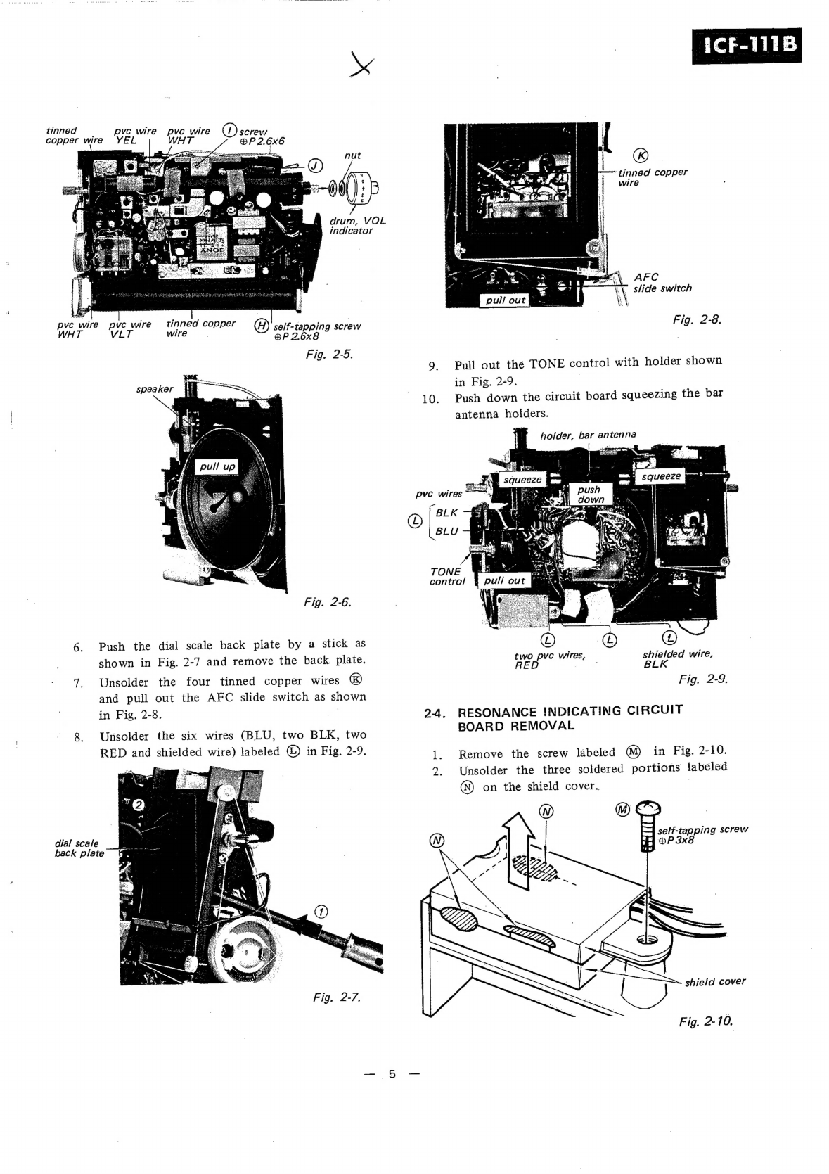
5
2-5.
Dial
Cord
Stringing
...................
seetanuaes
scuawedsastecdcieootearee
enealsscedenedeeemes
6
3.
CIRCUIT
ADJUSTMENTS
............
Hae
bs
6s
Gaaieiseadacaed
leone
vactaawsncussaesavciaianouneesoes
6
3-1.
Fm
If
Alignment
oo...
eee
ise
cist
cssheae
SacuTe
cise
was
earaneeee
Gataaenccsatiane
6
3-2.
A-m
I-f
Alignment
..........c.ccccsscecsssssondéccocssescnsetccencccetensenscsaseceoeaseneanccees
7
3-3.
Frequency
Coverage
and
Tracking
AGIUSEMENE
|
-ccessiiiviiaseccecce
ce
eesaes
see
7
3-4.
Current
Adjustment
..............
enoubeusende
yas
Sal
cuebdaan
ease
voie
da
vouenosvieadesnsvnese:
8
4.
SCHEMATIC
AND
MOUNTING
BINGHAM
atid
Boneh
eee
ae
oO
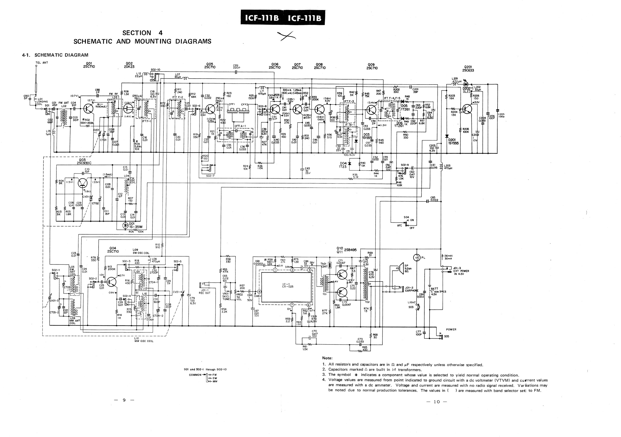
4].
“Schematic
Digsram
-
cccwcccseaisisecadedsatnss
ovaccwiagandecevasesevedusdsnoes
sesensweaeecepiae
9
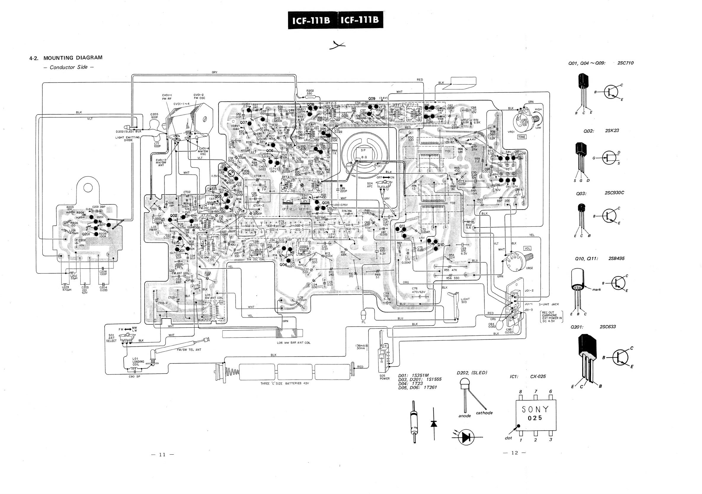
4-2.
Mounting
Diagram
—
Conductor
Side
—
ou.....eceeeccsceeeeeeceeeeeeceneeeen
ees
11
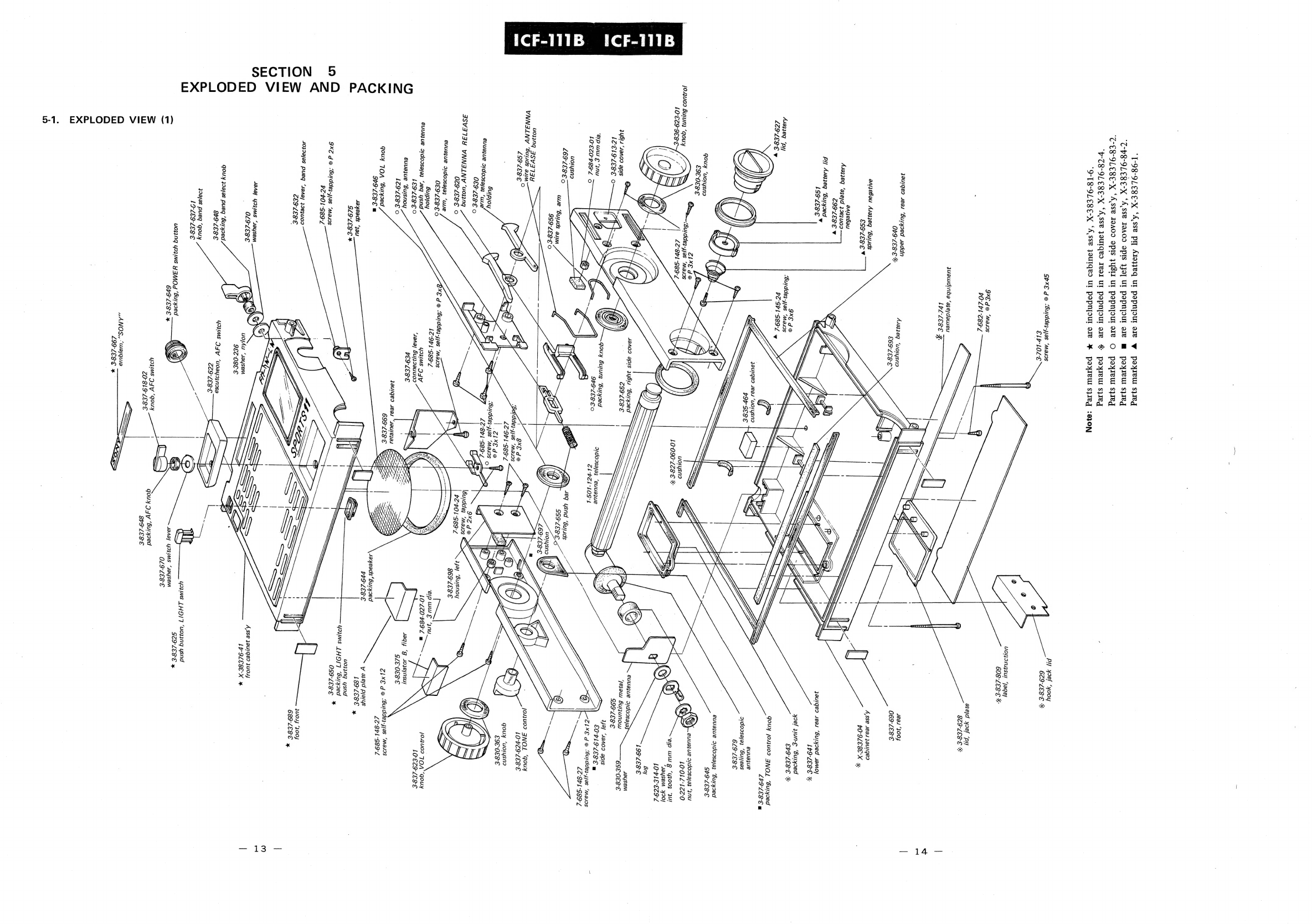
5.
EXPLODED
VIEW
AND
PACKING
.00:............
cc
ccesecsseccecceccesecescrecoscussencceees
13
5-1.
Exploded
View
(1)
wu.........eeceee
eee
Meee
sas
tae
eeauit
a
bam
ae
oane
mats
atiaea
ame
eeeeae
13
Se).
HEXPlOdEd
“VIEW
C2):
wicrscensecem
sc
esencuccoustecensacedenatisguisnedaceavengsasestauaveoasaecesees
15
Badie
“PAC
KIO
acts
ae)
ocnae
oa
nesta
sce
anuiewnas
Gaccaeisi
es
wien
buss
Gussuecues
bya
eodeeateerenieasienses
17
6.
ELECTRICAL:
PARES
[LEST
scscccscccicecicedecnticesatine
oincstiewdace
haga
eensancceesdcenau
es
18
SECTION
1
OUT
LINE
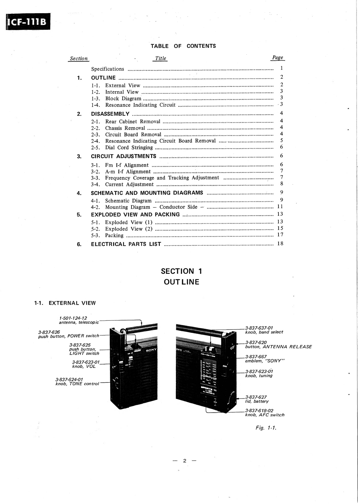
1-1.
EXTERNAL
VIEW
1-501-124-12
antenna,
telescopic
3-837-637-01
3-837-626
—
push
button,
POWER
switch
knob,
band
selec
227.
3-837-620
Deh
Bueoh
button,
ANTENNA
RELEASE
LIGHT
switch
3-837-667
3-837-623-01
emblem,
“SONY”
knob,
VOL
}
3-837-623-01
3-837-624-01
knob,
tuning
knob,
TONE
control
3-837-627
lid,
battery
3-837-618-02
knob,
AFC
switch
Fig.
1-7.