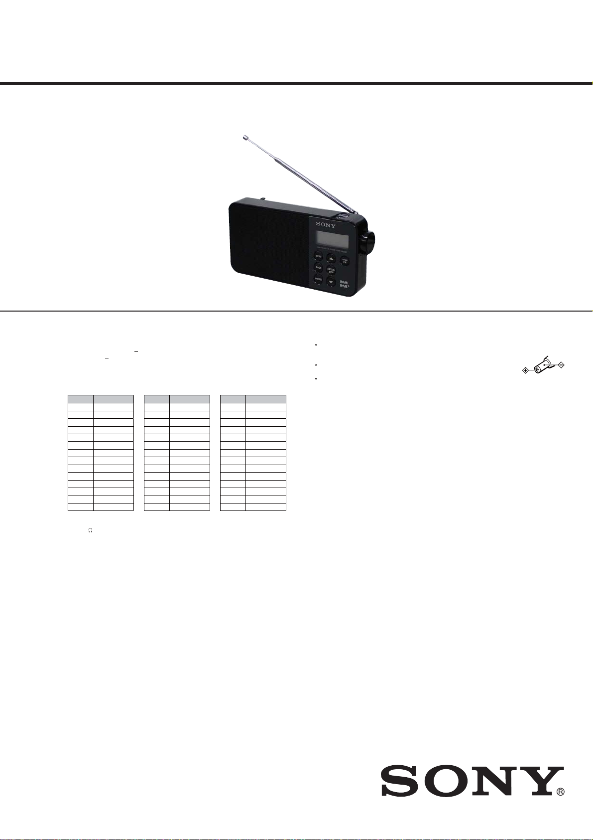
XDR-S40DBP
10
SECTION 3
TEST MODE
1. PREPARATION OF TEST MODE
Prepare the following before checking test mode.
• AC adaptor
• Regulated DC power supply
• Dry battery 4PCS. (SIZE “AA”, IEC designation LR6)
• Dummy battery
• Headphone
• Signal generator
• Oscilloscope
• Loop antenna
• Ammeter
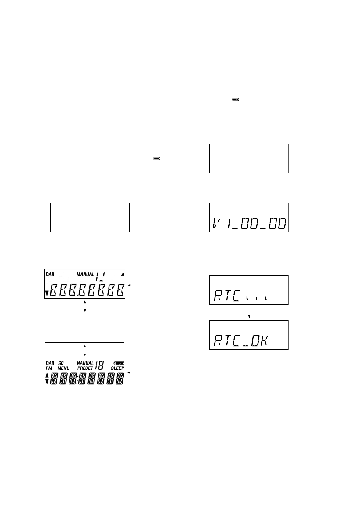
2. LCD CHECK
Procedure:
1. AC adaptor is inserted in DC jack (J201).
2. Press the [?/1] button to turn the power on.
3. Press the [DAB/FM] button, and checks that there is no “ ”
mark in the upper right of the liquid crystal display.
4. Press and hold the [?/1] button, while pressing the [MENU]
button.
5. Release the [MENU] button ([?/1] button is holding).
6. Press the [v], [V] button in order, and release the [?/1] button.
Enter the test mode and the “FW VER” appears.
7. Press the [v] or [V] buttons, select the “LCD CHK”, and press
the [ENTER/DISP] button.
8. The back light is turned on, and press the [v] or [V] buttons to
change the display pattern.
(Displayed characters in the following figure are example)
It checks that there are not contrast inconsistency and defective
indication.
9. Pull out the AC adaptor.
3. VERSION, RTC AND CURRENT CONSUMPTION
CHECK
Procedure:
1. Dummy battery is set to the unit, and it connects with a regu-
lated DC power supply, and outputs the voltage of 6V.
2. Telescopic antenna is set, and press the [?/1] button to turn the
power on.
Checks that there is “ ” mark in the upper right of the liquid
crystal display.
3. Press and hold the [?/1] button, while pressing the [MENU]
button.
4. Release the [MENU] button ([?/1] button is holding).
5. Press the [v], [V] button in order, and release the [?/1] button.
Enter the test mode and the “FW VER” appears.
6. Press the [ENTER/DISP] button to display the firmware ver-
sion.
(Displayed characters/values in the following figure are ex-
ample)
7. Press the [BACK] button, return to the test menu.
8. Press the [v] or [V] buttons, select the “RTC CHK”, and press
the [ENTER/DISP] button to start the RTC check.
The message “RTC_OK” appears on the liquid crystal display.
Press the [BACK] button, return to the test menu.
9. Press the [v] or [V] buttons, select the “INIT”, and press the
[ENTER/DISP] button twice to turn the power off.
10. Press the [?/1] button to turn the power on.
11. Press the [DAB/FM] button, change to DAB function.
Checks that current consumption is under 150 mA using an
ammeter.
12. Press the [DAB/FM] button, change to FM function.
Checks that current consumption is under 160 mA using an
ammeter.
13. Press the [?/1] button to turn the power off.
Checks that current consumption is under 30 μA using an am-
meter.
14. Remove dummy battery.
(Display is all off)
FW VER
FW VER