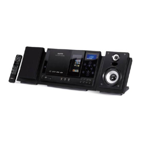
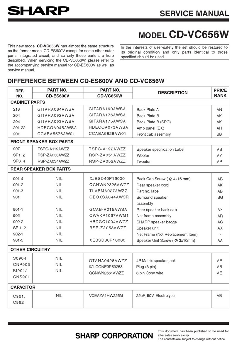
Sony FST-GTK11iP User manual

SERVICE MANUAL
Sony Corporation
Published by Sony Techno Create Corporation
SPECIFICATIONS
HOME AUDIO DOCKING SYSTEM
9-893-451-01
2012C33-1
© 2012.03
US Model
RDH-GTK33iP
AEP Model
UK Model
Saudi Arabia Model
Singapore Model
Malaysia Model
RDH-GTK11iP
E Model
FST-GTK11iP/GTK33iP
Australian Model
RDH-GTK11iP/GTK33iP
Chilean Model
Peruvian Model
FST-GTK33iP
Ver. 1.0 2012.03
FST-GTK11iP/GTK33iP/
RDH-GTK11iP/GTK33iP
License and Trademark Notice
iPhone, iPod, iPod classic, iPod nano, and iPod touch
are trademarks of Apple Inc., registered in the U.S. and
other countries.
MPEG Layer-3 audio coding technology and patents
licensed from Fraunhofer IIS and omson.
Windows Media is either a registered trademark or
trademark of Microso Corporation in the United
States and/or other countries.
is product contains technology subject to certain
intellectual property rights of Microso. Use or
distribution of this technology outside of this product
is prohibited without the appropriate license(s) from
Microso.
All other trademarks and registered trademarks are of
their respective holders. In this manual, ™and ®marks
are not specied.
Amplier section (Except US model)
e following are measured at AC 120 V 240 V, 50/60 Hz (Latin American
models (except for Mexican and Argentine models))
e following are measured at AC 127 V, 60 Hz (Mexican model)
e following are measured at AC 220 V 240 V, 50/60 Hz (European,
Russian, Australian and Argentine models)
e following are measured at AC 120 V 240 V, 50/60 Hz (Other models)
FST-GTK33iP/RDH-GTK33iP
Power output (rated):
100 W + 100 W (at 3.5 Ω, 1 kHz, 1% THD)
RMS output power (reference):
210 W + 210 W (per channel at 3.5 Ω, 1 kHz)
FST-GTK11iP/RDH-GTK11iP
Power output (rated):
55 W + 55 W (at 3 Ω, 1 kHz, 1% THD)
RMS output power (reference):
115 W + 115 W (per channel at 3 Ω, 1 kHz)
Speaker section
Speaker system: 2 way speaker system, Bass reex
Speaker units:
FST-GTK33iP/RDH-GTK33iP:
Woofer: 200 mm, cone type
Tweeter: 66 mm, cone type
FST-GTK11iP/RDH-GTK11iP:
Woofer: 160 mm, cone type
Tweeter: 40 mm, cone type
Rated impedance:
FST-GTK33iP/RDH-GTK33iP: 3.5 Ω
FST-GTK11iP/RDH-GTK11iP: 3.0 Ω
Input
DVD/PC IN (audio in L/R):
FST-GTK33iP/RDH-GTK33iP: Sensitivity 1,000 mV, impedance 47 kΩ
FST-GTK11iP/RDH-GTK11iP: Sensitivity 1,500 mV, impedance 47 kΩ
iPod/iPhone section
iPod/iPhone connector:
Output voltage: DC 5 V
Maximum output current: 1 A
Compatible iPod/iPhone models:
iPod touch 4th generation
iPod touch 3rd generation
iPod touch 2nd generation
iPod nano 6th generation
iPod nano 5th generation (video camera)
iPod nano 4th generation (video)
iPod nano 3rd generation (video)
iPod classic
iPhone 4S
iPhone 4
iPhone 3GS
iPhone 3G
“Made for iPod,” and “Made for iPhone” mean that an electronic accessory has
been designed to connect specically to iPod or iPhone, respectively, and has
been certied by the developer to meet Apple performance standards. Apple
is not responsible for the operation of this device or its compliance with safety
and regulatory standards. Please note that the use of this accessory with iPod
or iPhone may aect wireless performance.
USB section
Supported bit rates:
MP3 (MPEG 1 Audio Layer-3): 32 kbps 320 kbps, VBR
WMA: 48 kbps 192 kbps, VBR
AAC: 48 kbps 320 kbps
Sampling frequencies:
MP3 (MPEG 1 Audio Layer-3): 32/44.1/48 kHz
WMA: 44.1 kHz
AAC: 44.1 kHz
(USB) port: Type A, maximum current 500 mA
Tuner section
FM stereo, FM/AM superheterodyne tuner
Antenna:
FM lead antenna
AM loop antenna
FM tuner section:
Tuning range:
87.5 MHz 108.0 MHz (50 kHz step) (Except US model)
AM tuner section:
Tuning range:
European, Russian and Saudi Arabian models:
531 kHz 1,602 kHz (9 kHz step)
US and Latin American models:
530 kHz 1,710 kHz (10 kHz step)
531 kHz 1,710 kHz (9 kHz step)
Australian model:
531 kHz 1,710 kHz (9 kHz step)
530 kHz 1,710 kHz (10 kHz step)
Other models:
531 kHz 1,602 kHz (9 kHz step)
530 kHz 1,610 kHz (10 kHz step)
General
Power requirements:
Latin American models (except for Mexican and Argentine models):
AC
US model:
120 V 240 V, 50/60 Hz
Mexican model:
AC 127 V, 60 Hz
European, Russian, Australian and Argentine models:
AC 220 V 240 V, 50/60 Hz
Other models:
AC 120 V 240 V, 50/60 Hz
Power consumption:
FST-GTK33iP/RDH-GTK33iP: 75 W (0.5 W at the Power Saving mode)
FST-GTK11iP/RDH-GTK11iP: 45 W (0.5 W at the Power Saving mode)
Dimensions (W/H/D):
FST-GTK33iP/RDH-GTK33iP: Approx. 768.5 mm × 323 mm × 385 mm
FST-GTK11iP/RDH-GTK11iP: Approx. 678.5 mm × 323 mm × 385 mm
Mass:
FST-GTK33iP/RDH-GTK33iP: Approx. 14.0 kg
FST-GTK11iP/RDH-GTK11iP: Approx. 12.5 kg
Quantity of the unit: 1 piece
Supplied accessories: Remote Commander (1), R6 (Size AA) batteries (2),
FM lead/AM loop antenna (1)
Design and specications are subject to change without notice.
AUDIO POWER SPECIFICATIONS
POWER OUTPUT AND TOTAL HARMONIC DISTORTION:
(e United States model only)
With 3.5 ohm loads, both channels driven, from 120 10,000 Hz; rated
50 watts per channel minimum RMS power, with no more than 0.7% total
harmonic distortion from 250 milliwatts to rated output.
Amplier section (US model)
RMS output power (reference):
210 W + 210 W (per channel at 3.5 Ω, 1 kHz)
87.5 MHz 108.0 MHz (100 kHz step) (US model)
AC 120 V, 60 Hz
Photo: RDH-GTK33iP
FST-GTK11iP/GTK33iP/RDH-GTK11iP/GTK33iP
2
NOTES ON CHIP COMPONENT REPLACEMENT
• Never reuse a disconnected chip component.
• Notice that the minus side of a tantalum capacitor may be dam-
aged by heat.
SAFETY CHECK-OUT
After correcting the original service problem, perform the follow-
ing safety check before releasing the set to the customer:
Check the antenna terminals, metal trim, “metallized” knobs,
screws, and all other exposed metal parts for AC leakage.
Check leakage as described below.
LEAKAGE TEST
The AC leakage from any exposed metal part to earth ground and
from all exposed metal parts to any exposed metal part having a
return to chassis, must not exceed 0.5 mA (500 microamperes.).
Leakage current can be measured by any one of three methods.
1. A commercial leakage tester, such as the Simpson 229 or RCA
WT-540A. Follow the manufacturers’ instructions to use these
instruments.
2. A battery-operated AC milliammeter. The Data Precision 245
digital multimeter is suitable for this job.
3. Measuring the voltage drop across a resistor by means of a
VOM or battery-operated AC voltmeter. The “limit” indication
is 0.75 V, so analog meters must have an accurate low-voltage
scale. The Simpson 250 and Sanwa SH-63Trd are examples
of a passive VOM that is suitable. Nearly all battery operated
digital multimeters that have a 2 V AC range are suitable. (See
Fig. A)
1.5 kΩ0.15 μF
AC
voltmeter
(0.75 V)
To Exposed Metal
Parts on Set
Earth Ground
Fig. A. Using an AC voltmeter to check AC leakage.
SAFETY-RELATED COMPONENT WARNING!
COMPONENTS IDENTIFIED BY MARK 0OR DOTTED LINE
WITH MARK 0ON THE SCHEMATIC DIAGRAMS AND IN
THE PARTS LIST ARE CRITICAL TO SAFE OPERATION.
REPLACE THESE COMPONENTS WITH SONY PARTS
WHOSE PART NUMBERS APPEAR AS SHOWN IN THIS
MANUAL OR IN SUPPLEMENTS PUBLISHED BY SONY.

FST-GTK11iP/GTK33iP/RDH-GTK11iP/GTK33iP
3
1. SERVICING NOTES ............................................. 4
2. DISASSEMBLY
2-1. Disassembly Flow........................................................... 12
2-2. Side Panel (R) ................................................................. 13
2-3. Side Panel (L-base)......................................................... 14
2-4. Cover (Back) Block ........................................................ 15
2-5. Back Panel Block (GTK11iP)......................................... 16
2-6. Back Panel Block (GTK33iP)......................................... 17
2-7. Shield (Main) Block........................................................ 18
2-8. Panel Right Assy............................................................. 19
2-9. USB Board...................................................................... 20
2-10. Stage (Bottom-i-ph) Block.............................................. 20
2-11. Spring (PWB) ................................................................. 21
2-12. IP Board .......................................................................... 21
2-13. Spring (Lock 2) ............................................................... 22
2-14. MAIN Board ................................................................... 23
2-15. Shield (Power) Block...................................................... 24
2-16. Power Cord (AC1) .......................................................... 25
2-17. GTK11-SMPS Board (GTK11iP) /
GTK33-SMPS Board (GTK33iP)................................... 26
2-18. Chassis Block, Reinforcement (Back Panel) Block ....... 27
2-19. Ornament Base Block ..................................................... 27
2-20. Front Panel Assy ............................................................. 28
2-21. Loudspeaker (16 cm) (SP1, AP2) (GTK11iP) ................ 29
2-22. Loudspeaker (20 cm) (SP1, AP2) (GTK33iP) ................ 30
3. TEST MODE ............................................................ 31
4. ELECTRICAL CHECK ......................................... 32
5. DIAGRAMS
5-1. Block Diagram - MAIN Section -................................... 33
5-2. Block Diagram - AMP Section - ..................................... 34
5-3. Block Diagram - REGULATOR Section -...................... 35
5-4. Block Diagram - POWER SUPPLY Section -................ 36
5-5. Printed Wiring Board
- MAIN Board (Component Side) -................................ 38
TABLE OF CONTENTS
5-6. Printed Wiring Board
- MAIN Board (Conductor Side) -.................................. 39
5-7. Schematic Diagram - MAIN Board (1/4) -..................... 40
5-8. Schematic Diagram - MAIN Board (2/4) -..................... 41
5-9. Schematic Diagram - MAIN Board (3/4) -..................... 42
5-10. Schematic Diagram - MAIN Board (4/4) - ..................... 43
5-11. Printed Wiring Boards - AUDIO INPUT Section - ........ 44
5-12. Schematic Diagram - AUDIO INPUT Section -............. 45
5-13. Printed Wiring Boards - PANEL Section - ..................... 46
5-14. Schematic Diagram - PANEL Section -.......................... 47
5-15. Printed Wiring Board
- GTK11-SMPS Board - (GTK11iP) .............................. 48
5-16. Schematic Diagram
- GTK11-SMPS Board - (GTK11iP) .............................. 49
5-17. Printed Wiring Board
- GTK33-SMPS Board - (GTK33iP) .............................. 50
5-18. Schematic Diagram
- GTK33-SMPS Board - (GTK33iP) .............................. 51
6. EXPLODED VIEWS
6-1. Side Panel Section .......................................................... 61
6-2. Back Cover Section ........................................................ 62
6-3. Back Panel Section (GTK11iP) ...................................... 63
6-4. Back Panel Section (GTK33iP) ...................................... 64
6-5. Ornament Section ........................................................... 65
6-6. Top Panel Section ........................................................... 66
6-7. Front Panel Section......................................................... 67
6-8. DC Fan Section............................................................... 68
6-9. MAIN Board Section ...................................................... 69
6-10. Chassis Section ............................................................... 70
6-11. SPK Box Section (GTK11iP) ......................................... 71
6-12. SPK Box Section (GTK33iP) ......................................... 72
6-13. LED Board Section ......................................................... 73
7. ELECTRICAL PARTS LIST .............................. 74
Accessories are given in the last of the electrical parts list.

FST-GTK11iP/GTK33iP/RDH-GTK11iP/GTK33iP
4
SECTION 1
SERVICING NOTES
UNLEADED SOLDER
Boards requiring use of unleaded solder are printed with the lead-
free mark (LF) indicating the solder contains no lead.
(Caution: Some printed circuit boards may not come printed with
the lead free mark due to their particular size)
: LEAD FREE MARK
Unleaded solder has the following characteristics.
• Unleaded solder melts at a temperature about 40 °C higher
than ordinary solder.
Ordinary soldering irons can be used but the iron tip has to be
applied to the solder joint for a slightly longer time.
Soldering irons using a temperature regulator should be set to
about 350 °C.
Caution: The printed pattern (copper foil) may peel away if
the heated tip is applied for too long, so be careful!
• Strong viscosity
Unleaded solder is more viscous (sticky, less prone to flow)
than ordinary solder so use caution not to let solder bridges
occur such as on IC pins, etc.
• Usable with ordinary solder
It is best to use only unleaded solder but unleaded solder may
also be added to ordinary solder.
MODEL IDENTIFICATION
– Bottom side view –
Model No.
OME AUDIO DOCKING SYSTEM
R
Power requirements
Displayed characters/
values are example.
The written example of
model number label.
Displayed characters/
values are example.
The written example of
stamp.
Power requirements
Model Power requirements
GTK11iP: AEP, UK, AUS AC:220 - 240V -50/60Hz 45W
GTK11iP: RU -220 - 240V 50/60Hz 45W
GTK11iP: E2, EA, SP6 AC:120 - 240V -50/60Hz 45W
GTK11iP: MX ca 127 V -60 Hz 45 W
GTK33iP: US AC:120V -60Hz 75W
GTK33iP: E2, E51 AC:120 - 240V -50/60Hz 75W
GTK33iP: MX ca 127 V -60 Hz 75 W
GTK33iP: AUS AC:220 - 240V -50/60Hz 75W
• Abbreviation
AUS : Australian model
E2 : 120V AC area in E model
E51 : Chilean and Peruvian models
EA : Saudi Arabia model
MX : Mexican model
RU : Russian model
SP6 : Singapore and Malaysia models
NOTE THE D009 AND D010 ON THE LED (L) BOARD
REPLACING
D009 and D010 on the LED (L) board cannot exchange with
single. When these parts are damaged, exchange the complete
mounted board.
NOTE THE D009 AND D010 ON THE LED (R) BOARD
REPLACING
D009 and D010 on the LED (R) board cannot exchange with
single. When these parts are damaged, exchange the complete
mounted board.
THE OPERATION CHECK AFTER REPAIR
After repair is completed, connect corresponding “iPhone” etc.
to this unit and perform operation checks (playback, recording,
charging, etc.).
NOTE OF PERFORMING THE OPERATION CHECK
Don’t perform the operation check in the state where the heat sink
was removed from this unit, by any means. When the operation
check is performed, be sure to fix the heat sink to the board in
advance.
NOTE OF REPLACING THE IC702 ON THE MAIN
BOARD AND THE COMPLETE MAIN BOARD
When IC702 on the MAIN board and the complete MAIN board
are replaced, it is necessary to spread the compound between parts
and heat sink.
Part No. Description
J-2501-221-A THERMAL COMPOUND (G747)
Spread the compound referring to the figure below.
IC702
– MAIN Board (Component Side) –
IC702

FST-GTK11iP/GTK33iP/RDH-GTK11iP/GTK33iP
5
CAPACITOR ELECTRICAL DISCHARGE PROCESSING
When checking the board, the electrical discharge is necessary for
the electric shock prevention.
Connect the resistors referring to the figure below.
• Connetion position
1. MAIN board (Ref. No. C734) (page 5)
2. GTK11-SMPS board (Ref. No. C914) (GTK11iP only)
(page 5)
3. GTK33-SMPS board (Ref. No. C914) (GTK33iP only)
(page 6)
1. MAIN board (Ref. No. C734)
The MAIN board can be discharged by two kinds of following
methods.
1. Both ends of C734.
– MAIN Board (Conductor Side) –
C734
C734
800 :/2 W
2. Ground terminal (ET703) and R727.
Note: When you use this connection, confirm that the GTK11-SMPS
board (GTK11iP) or the GTK33-SMPS board (GTK33iP) is not
connected with CN811 on the MAIN board.
– MAIN Board (Component Side) –
CN811
Not connect
0 :
R727
ET703
R727
ET703
2. GTK11-SMPS board (Ref. No. C914) (GTK11iP only)

The GTK11-SMPS board can be discharged by two kinds of fol-
lowing methods.
1. Both ends of C914.
– GTK11-SMPS Board (Conductor Side) –
C914
C914
800 :/2 W
2. Heat sink (A930) and R914.
– GTK11-SMPS Board (Component Side) –
A930
0 :
R914
A930
R914

FST-GTK11iP/GTK33iP/RDH-GTK11iP/GTK33iP

6
3. GTK33-SMPS board (Ref. No. C914) (GTK33iP only)
The GTK33-SMPS board can be discharged by two kinds of fol-
lowing methods.
1. Both ends of C914.
– GTK33-SMPS Board (Conductor Side) –
C914
C914
800 :/2 W
2. Heat sink (A930) and R914.
A930
0 :
– GTK33-SMPS Board (Component Side) –
R914
R914
A930
BOND FIXATION OF ELECTRIC PARTS
When MAIN board is replaced or the following object parts are
replaced, it is necessary to fix parts to the boards by using a speci-
fied bond without fail.
• Object boards
Complete MAN board
• Object parts
Board Ref. No.
GTK11-SMPS C905, C914, C967, C969, L903, L904, R933,
R934, T901, VDR901
GTK33-SMPS C905, C911, C912, C914, C943, C944, C986,
L901, L902, R930, R931, T901, T903, VDR901
MAIN
C730, C731, C732, C733, C734, C811, L703,
L704, L705, L706, L707, L708, L709, L710,
R727
• Use bond
Part No. Description
7-432-912-52 BOND, SONY (SC-608LV)
• Parts position
1. MAIN board (page 7)
2. GTK11-SMPS board (GTK11iP only) (page 8)
3. GTK33-SMPS board (GTK33iP only) (page 9)

FST-GTK11iP/GTK33iP/RDH-GTK11iP/GTK33iP
7
1. MAIN board
– MAIN Board (Component Side) –
C811
C734
C734
J301
HS1
C730 L703
L707
L708
L709
L710
L704
L705
L706
C731
C732
C733
R727
The portion which applies bond:

FST-GTK11iP/GTK33iP/RDH-GTK11iP/GTK33iP
8
2. GTK11-SMPS board (GTK11iP only)
– GTK11-SMPS Board (Component Side) –
C905
VDR901
C914
A930
A931
C967
T901
R933
R934
C969
Fix the 180-degree or larger
circumferences of C914.
Fix the 90-degree or larger
circumferences of C967.
Fix the 90-degree or larger
circumferences of C969.
Fix both the sides of
L903 and L904 with the board.
Fix both the sides of
T901 with the board.
Fix A931 with the board.
Fix A930 with the board.
Fix R933 and R934
with the board.
Apply bond on
C905 and VDR901.
L904
L903
The portion which applies bond:

FST-GTK11iP/GTK33iP/RDH-GTK11iP/GTK33iP
9
3. GTK33-SMPS board (GTK33iP only)
– GTK33-SMPS Board (Component Side) –
A932A930
L902
L901
C905
VDR901
A931
C986
C944 C943
T901
T903
R930
R931
C914
C911
C912
Fix the 180-degree or larger
circumferences of C914, and
fix C911 and C912 with the board.
Fix circumferences of C986.
Fix circumferences of C943 and C944.
Fix both the sides of
L901 and L902 with the board.
Fix A930 with the board.
Fix A931 with the board.
Fix T901 with the board.
Fix T903 with the board.Fix R930 and R931 with the board.
Fix A932 with the board.
Apply bond on
C905 and VDR901.
The portion which applies bond:

FST-GTK11iP/GTK33iP/RDH-GTK11iP/GTK33iP
10
MAIN BOARD SERVICE POSITION
GTK11-SMPS/GTK33-SMPS BOARD SERVICE POSITION
MAIN board
GTK11-SMPS board (GTK11iP)/
GTK33-SMPS board (GTK33iP)
Note: Please spread a sheet under a unit
not to injure front grille.
– Top rear view –
MAIN board
GTK11-SMPS board (GTK11iP)/
GTK33-SMPS board (GTK33iP)
Note: Please spread a sheet under a uni
t
not to injure front grille.
–
Top rear view –

FST-GTK11iP/GTK33iP/RDH-GTK11iP/GTK33iP
11
PANEL BOARD, IP BOARD, USB BOARD SERVICE POSITION
LED BOARD SERVICE POSITION
MAIN board
USB board
IP board
PANEL board
– Rear left view –
LED board
LED board
–
Front left view –

FST-GTK11iP/GTK33iP/RDH-GTK11iP/GTK33iP
12
SECTION 2
DISASSEMBLY
• This set can be disassembled in the order shown below.
2-1. DISASSEMBLY FLOW
SET
2-2. SIDE PANEL (R)
(Page 13)
2-3. SIDE PANEL (L-BASE)
(Page 14)
2-13. SPRING (LOCK 2)
(Page 22)
2-4. COVER (BACK) BLOCK
(Page 15)
2-7. SHIELD (MAIN) BLOCK
(Page 18)
2-8. PANEL RIGHT ASSY
(Page 19)
2-9. USB BOARD
(Page 20)
2-14. MAIN BOARD
(Page 23)
2-15. SHIELD (POWER) BLOCK
(Page 24)
2-16. POWER CORD (AC1)
(Page 25)
2-19. ORNAMENT BASE BLOCK
(Page 27)
2-20. FRONT PANEL ASSY
(Page 28)
2-18. CHASSIS BLOCK,
REINFORCEMENT (BACK PANEL) BLOCK
(Page 27)
2-17. GTK11-SMPS BOARD (GTK11iP)/
GTK33-SMPS BOARD (GTK33iP)
(Page 26)
2-10. STAGE (BOTTOM-I-PH)
BLOCK
(Page 20)
2-11. SPRING (PWB)
(Page 21)
2-12. IP BOARD
(Page 21)
2-5. BACK PANEL BLOCK (GTK11iP)
(Page 16)
2-6. BACK PANEL BLOCK (GTK33iP)
(Page 17)
2-21. LOUDSPEAKER (16 cm) (SP1, AP2) (GTK11iP)
(Page 29)
2-22. LOUDSPEAKER (20 cm) (SP1, AP2) (GTK33iP)
(Page 30)

FST-GTK11iP/GTK33iP/RDH-GTK11iP/GTK33iP
13
Note: Follow the disassembly procedure in the numerical order given.
2-2. SIDE PANEL (R)
2cover screw
tweezers etc.
6side panel (R)
5two cushions (E)
5two cushions (E)
slot
slot
slot
slot
slot
slot
2cover screw
2cover screw
2cover screw
3screw
(BVTP3 u10)
3screw
(BVTP3 u10)
3screw
(BVTP3 u10)
3screw
(BVTP3 u10)
&RYHUVFUHZVHWWLQJ
:LUHVHWWLQJ
slot
slot
1Insert tweezers etc. in the slot on four cover
screws and remove so that it may hollow.
Note: Do not damage cover screw.
–,QQHUYLHZ––2XWHUYLHZ–
–,QQHUYLHZ––2XWHUYLHZ– –,QQHUYLHZ––2XWHUYLHZ–
–,QQHUYLHZ––2XWHUYLHZ–
–5LJKWVLGHYLHZ–
–5LJKWVLGHYLHZ–
4Remove the side
panel (R) block in
the direction of an
arrow.

FST-GTK11iP/GTK33iP/RDH-GTK11iP/GTK33iP
14
2-3. SIDE PANEL (L-BASE)
2foot
6side panel (L-base)
2foot
2foot
5foot (bottom) 5foot
(bottom) 2foot
– Rear left view –
– Left side view –
3tapping screw
(3.5 u20) 3tapping screw
(3.5 u20)
3tapping screw
(3.5 u20)
3tapping screw
(3.5 u20)
:ire settiQJ
1Insert tweezers etc. in the slot on four foots
and remove so that it may hollow.
Note: Do not damage foot.
tweezers etc.
4Remove the side panel (L-base) block
in the direction of an arrow.

FST-GTK11iP/GTK33iP/RDH-GTK11iP/GTK33iP
15
2-4. COVER (BACK) BLOCK
– Top rear view –
– Right side view –
8cover (back) block
5Move the cover (back) block
in the direction of an arrow.
6Remove the cover (back)
block in the direction of
an arrow.
2screw (BV/ring)
2screw
(BV/ring)
3two lug wires
tape
rear side
top side
45 ± 5 mm
tape
1three tapping screws
(3.5 u20)
4screw
(BVTP3 u10) 4screw
(BVTP3 u10)
Wire setting
Note 1: Please spread a sheet under a unit
not to injure front grille.
Note 2: When installing the flexible
flat cable, ensure the coloured
line.
No slanting after insertion.
coloured line
coloured line
Insert is straight to the interior.
Insert is incline
flexible flat
cable
flexible flat
cable
connector
connector
OK
NG
Distance
is near.
OK NG
Distance
is far.
7flexible flat cable (9 core)
(CN101)

FST-GTK11iP/GTK33iP/RDH-GTK11iP/GTK33iP
16
2-5. BACK PANEL BLOCK (GTK11iP)
2cord bushing (2104)
1Remove the power cord.
0back panel
block
7four screw caps
7four screw
caps
4four claws
4four claws
4four claws
4four claws
5screw cover (back panel)
5screw cover
(back panel)
5screw cover
(back panel)
– Top rear view –
Note 3: Please spread a sheet under a unit
not to injure front grille.
8four screws
(BVTP3 u10)
8four screws
(BVTP3 u10)
8two screws
(BVTP3 u10)
9tapping screw
(3.5 u20)
9tapping screw
(3.5 u20)
9two tapping screws
(3.5 u20)
tweezers etc.
tweezers etc.
3Insert tweezers etc. in the slot on four screw
covers (back panel) and remove so that it may hollow.
Note 1: Do not damage screw cover (back panel).
6Insert tweezers etc. in the slot on eight screw
caps and remove so that it may hollow.
Note 2: Do not damage screw cap.
cord bushing (2104)
ferrite core
power cord
290 ± 5 mm
Power cord setting

FST-GTK11iP/GTK33iP/RDH-GTK11iP/GTK33iP
17
2-6. BACK PANEL BLOCK (GTK33iP)
2cord bushing (2104)
1Remove the power cord.
4four claws
4four claws
5screw cover (back panel)
5screw cover
(back panel)
9two tapping screws
(3.5 u20)
0back panel
block
7five screw caps
7five screw caps
4four claws
4four claws
5screw cover (back panel)
5screw cover
(back panel)
8five screws
(BVTP3 u10)
8five screws
(BVTP3 u10)
8two screws
(BVTP3 u10)
9tapping screw
(3.5 u20)
9tapping screw
(3.5 u20)
– Top rear view –
Note 3: Please spread a sheet under a unit
not to injure front grille.
cord bushing (2104)
ferrite core
power cord
290 ± 5 mm
Power cord setting
tweezers etc.
tweezers etc.
3Insert tweezers etc. in the slot on four screw
covers (back panel) and remove so that it may hollow.
Note 1: Do not damage screw cover (back panel).
6Insert tweezers etc. in the slot on ten screw
caps and remove so that it may hollow.
Note 2: Do not damage screw cap.

FST-GTK11iP/GTK33iP/RDH-GTK11iP/GTK33iP
18
2-7. SHIELD (MAIN) BLOCK
– Top right view –
Note: Please spread a sheet under a unit
not to injure front grille.
(GTK33iP)
1screw (BV/ring)
3screw (BV/ring)
3screw (BV/ring)
3screw (BV/ring)
3screw (BV/ring)
1two screws (BV/ring)
3two screws (BV/ring)
3three screws (BV/ring)
2shield (main-U)
4shield (main) block

FST-GTK11iP/GTK33iP/RDH-GTK11iP/GTK33iP
19
2-8. PANEL RIGHT ASSY
1flexible flat cable (13 core)
(CN501)
2connector
(CN301)
4two bosses
4three bosses
5panel right assy
– Bottom right view –
Note 1: Please spread a sheet under a unit
not to injure front grille.
3five tapping screws
(3.5 u20)
3two tapping screws
(3.5 u20)
3tapping screw
(3.5 u20)
Note 3: When installing the flexible flat cable, ensure the coloured line.
No slanting after insertion.
coloured line coloured line
Insert is straight to the interior. Insert is incline
flexible flat
cable
flexible flat
cable
connectorconnector
OK NG
Note 2: When you install the connector, please install themcorrectly.
There is a possibility that this machine damages when not
correctly installing it.
Insert is shallow
Insert is straight
to the interior.
connector
Insert is incline
connector connector connector
connector connector
NGOK NG

FST-GTK11iP/GTK33iP/RDH-GTK11iP/GTK33iP
20
2-10. STAGE (BOTTOM-I-PH) BLOCK
2-9. USB BOARD
1two screws
(BVTP2.6)
4USB board
3connector (CN562)
2Remove the USB board in
the direction of an arrow.
Insert is shallow
Insert is straight
to the interior.
connector
Insert is incline
connector connector connector
connector connector
NGOK NG
– Panel right assy rear view –
Note: When you install the connector, please install themcorrectly.
There is a possibility that this machine damages when not
correctly installing it.
2two screws
(BVTP2.6)
3stage (bottom-I-PH) block
1two screws
(BTP2.6 u8)
– Panel right assy rear view –
This manual suits for next models
3
Table of contents
Other Sony Stereo System manuals

Sony
Sony MHC-EX66 User manual

Sony
Sony MHC-BX6AV User manual

Sony
Sony CMT-CNEZ3 User manual

Sony
Sony HCD-CX4iP User manual

Sony
Sony LBT-GV10AV User manual

Sony
Sony MHC-RX90 User manual

Sony
Sony LBT-ZX8 - Mini Hi-fi Component System User manual

Sony
Sony GTK-X1BT User manual

Sony
Sony LBT-ZUX10D User manual

Sony
Sony CMT HPZ7 User manual

Sony
Sony HCD-RG55 User manual

Sony
Sony SRS-XB3 User manual

Sony
Sony MHC-GX99 User manual

Sony
Sony CMT-SP55MD User manual

Sony
Sony HCD-GRX3 User manual

Sony
Sony HCD-BX3 User manual

Sony
Sony LBT-DR5 User manual

Sony
Sony MEX-BT3100P User manual

Sony
Sony MHC-GRX5 User manual

Sony
Sony CMT-CP1 - Micro Hi Fi Component System User manual