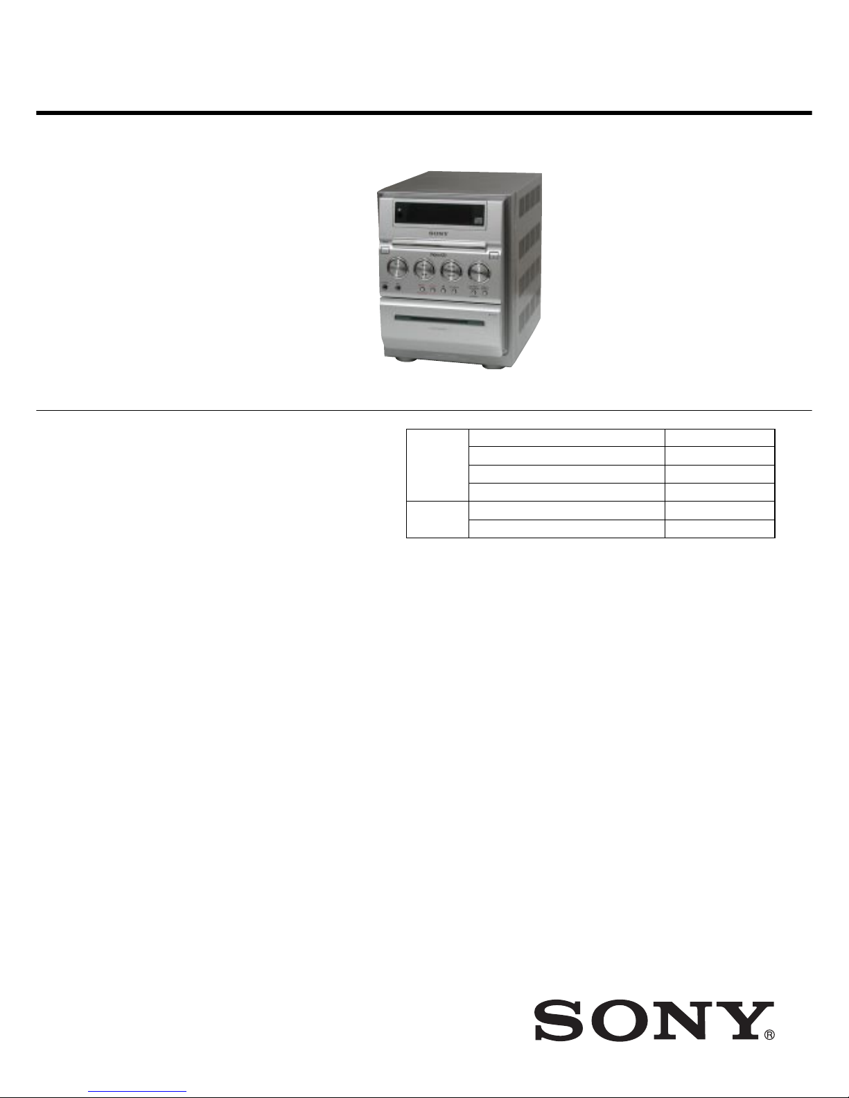
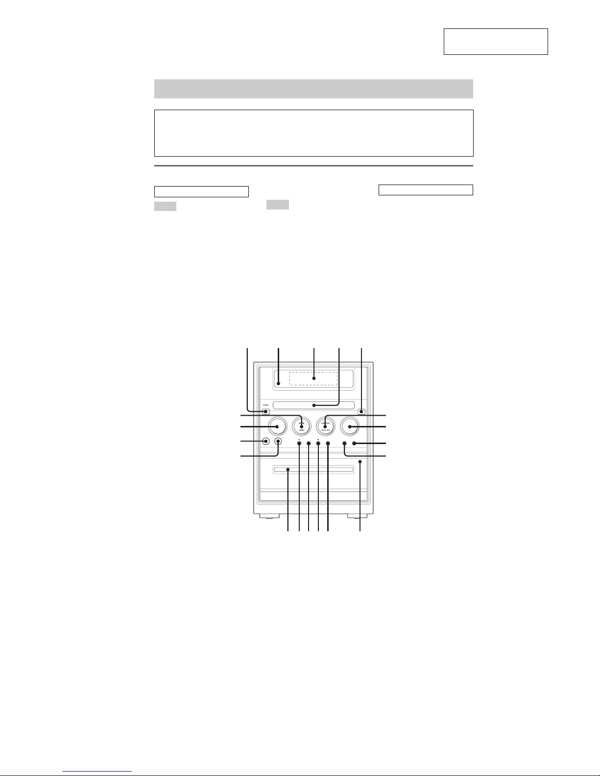
Sony HCD-GP6V User manual

SERVICE MANUAL
Sony Corporation
Audio Group
Published by Sony Engineering Corporation
E Model
MICRO HI-FI COMPONENT SYSTEM
9-877-654-03
2004I16-1
© 2004.09
Ver 1.2 2004.09
SPECIFICATIONS
HCD-GP6V
Model Name Using Similar Mechanism CX-LFAV500
CD CD Mechanism Type CDM55A-30BD61S
Section Base Unit Name BU-30BD61S
Optical Pick-up Name A-MAX.3
Tape deck Model Name Using Similar Mechanism HCD-GP5
Section Tape Transport Mechanism Type CMAL1Z240A
HCD-GP6V is the Amplifier, Video CD/CD player,
Tape Deck and Tuner section in CMT-GP6V.
— Continued on next page —
Amplifier section
The following measured at AC 240 V or AC 120 V, 50/
60 Hz
DIN power output (rated): 20 + 20 W
(6 ohms at 1 kHz, DIN)
Continuous RMS power output (reference):
30 + 30 W
(6 ohms at 1 kHz, 10%
THD)
Inputs
MD IN (phono jacks): Sensitivity 500 mV,
impedance 47 kilohms
MIC (phone jack): Sensitivity 1 mV,
impedance 10 kilohms
Outputs
PHONES (stereo minijack):
Accepts headphones with
an impedance of 8 ohms or
more
VIDEO OUT (phono jack):Max. output level 1Vp-p,
unbalanced, Sync
negative, load impedance
75 ohms
SPEAKERS: Accepts impedance of 6 to
16 ohms.
VIDEO CD/CD player section
System Compact disc and digital
audio system
Laser Semiconductor laser
(λ=780 nm)
Emission duration:
continuous
Frequency response 2 Hz – 20 kHz (±0.5 dB)
Wavelength 780 – 790 nm
Signal-to-noise ratio More than 90 dB
Dynamic range More than 90 dB
Video color system format NTSC, PAL
Tape deck section
Recording system 4-track 2-channel stereo
Frequency response 50 – 13,000 Hz (±3 dB),
using Sony TYPE I
cassettes

2
HCD-GP6V
Tuner section
FM stereo, FM/AM superheterodyne tuner
FM tuner section
Tuning range 87.5 – 108.0 MHz
(50-kHz step)
Antenna FM lead antenna
Antenna terminals 75 ohms balanced
Intermediate frequency 10.7 MHz
AM tuner section
Tuning range
Middle Eastern model: 531 – 1,602 kHz
(with the tuning interval
set at 9 kHz)
Other models: 530 – 1,710 kHz
(with the tuning interval
set at 10 kHz)
531 – 1,602 kHz
(with the tuning interval
set at 9 kHz)
Antenna AM loop antenna, external
antenna terminal
Intermediate frequency 450 kHz
General
Power requirements
Saudi Arabian model: 120 – 127/220 V AC, 50/
60 Hz
Adjustable with voltage
selector
Other models: 110 –120/220–240V AC,
50/60 Hz
Adjustable with voltage
selector
Power consumption 70 watts
Dimensions (w/h/d) Approx. 190 ×250 ×295
mm
Mass Approx. 4.7 kg
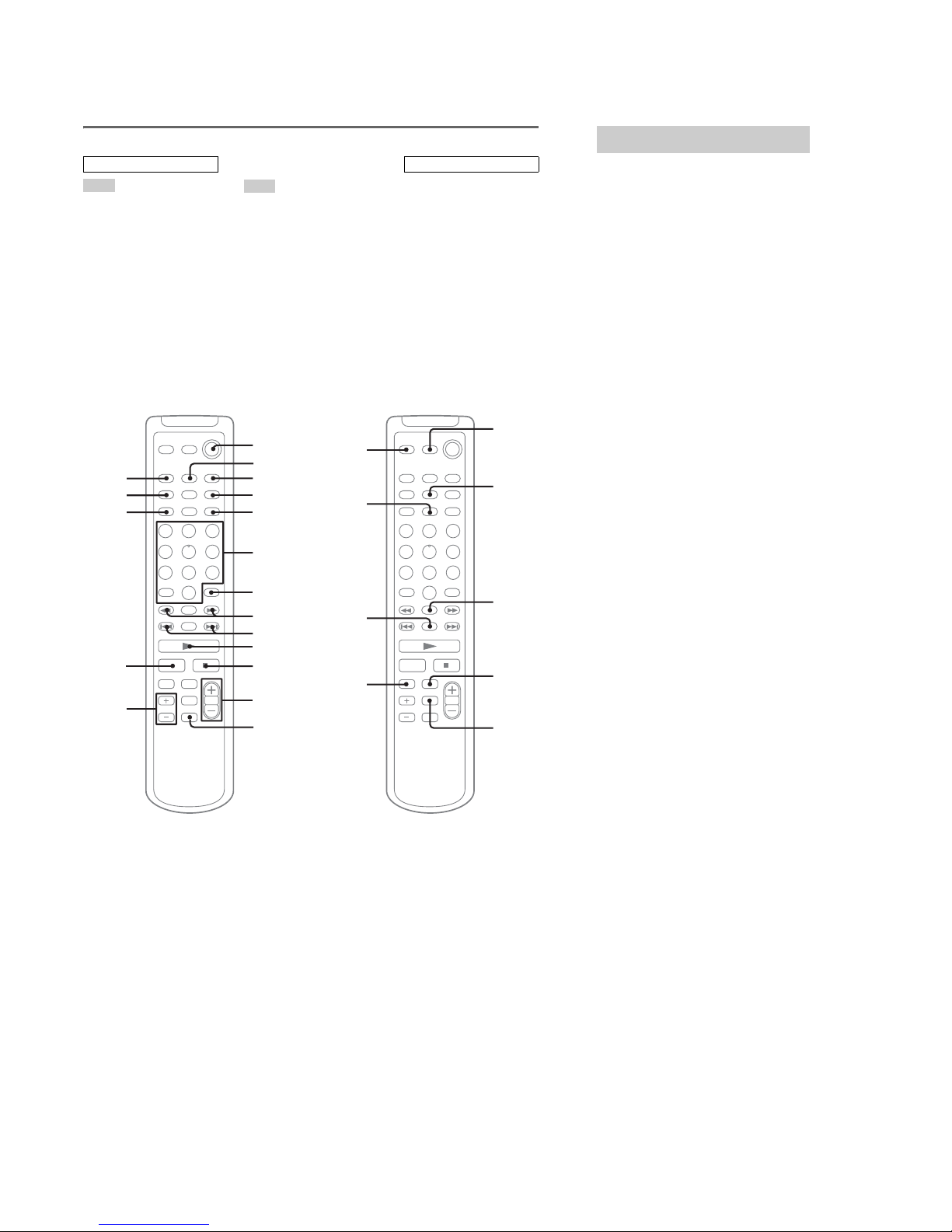
Supplied accessories Remote (1)
R6 (size AA) batteries (2)
AM loop antenna (1)
FM lead antenna (1)
Video cable (1)
Design and specifications are subject to change
without notice.
TABLE OF CONTENTS
1. SERVICING NOTES ................................................ 3
2. GENERAL ................................................................... 5
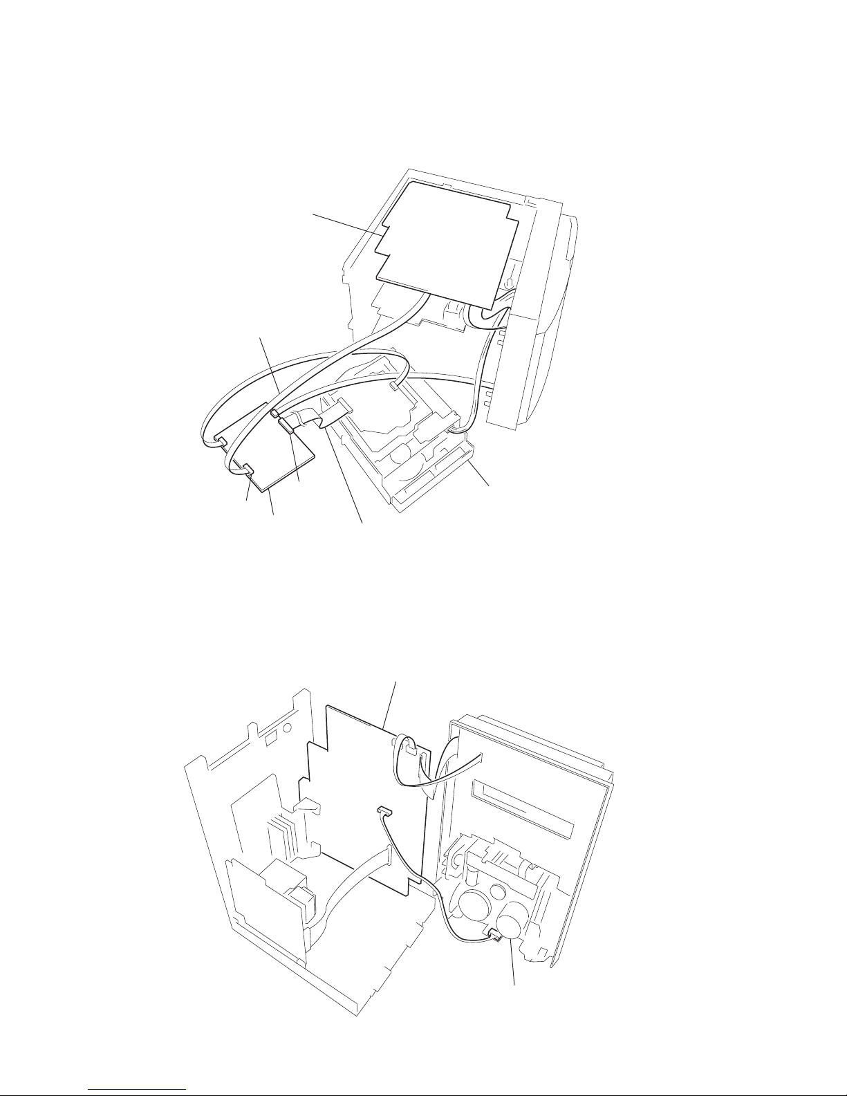
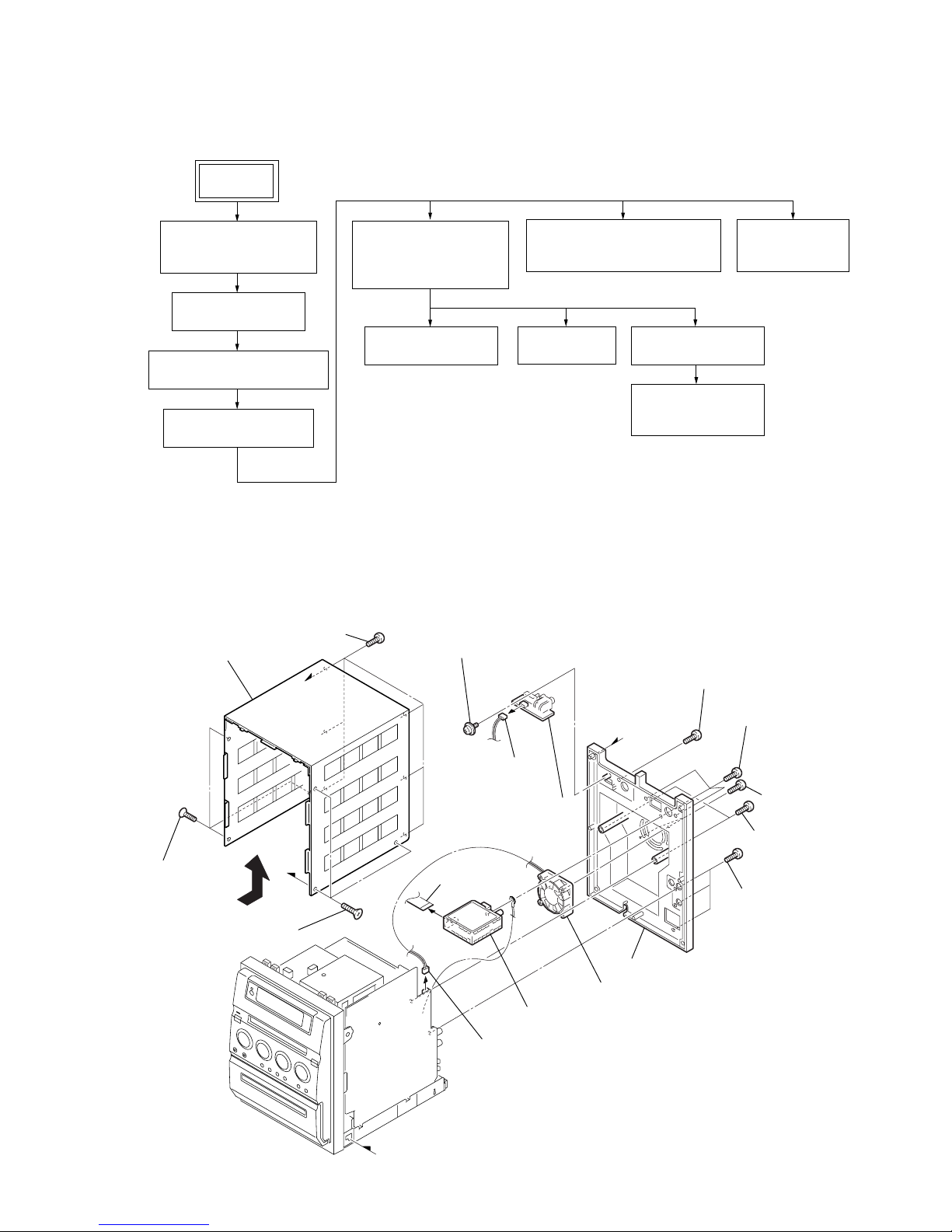
3. DISASSEMBLY
3-1. Top Cabinet, V-OUT Board, DC Fan .............................. 7
3-2. MIC/ECHO Board........................................................... 8
3-3. CD Mechanism Section................................................... 8
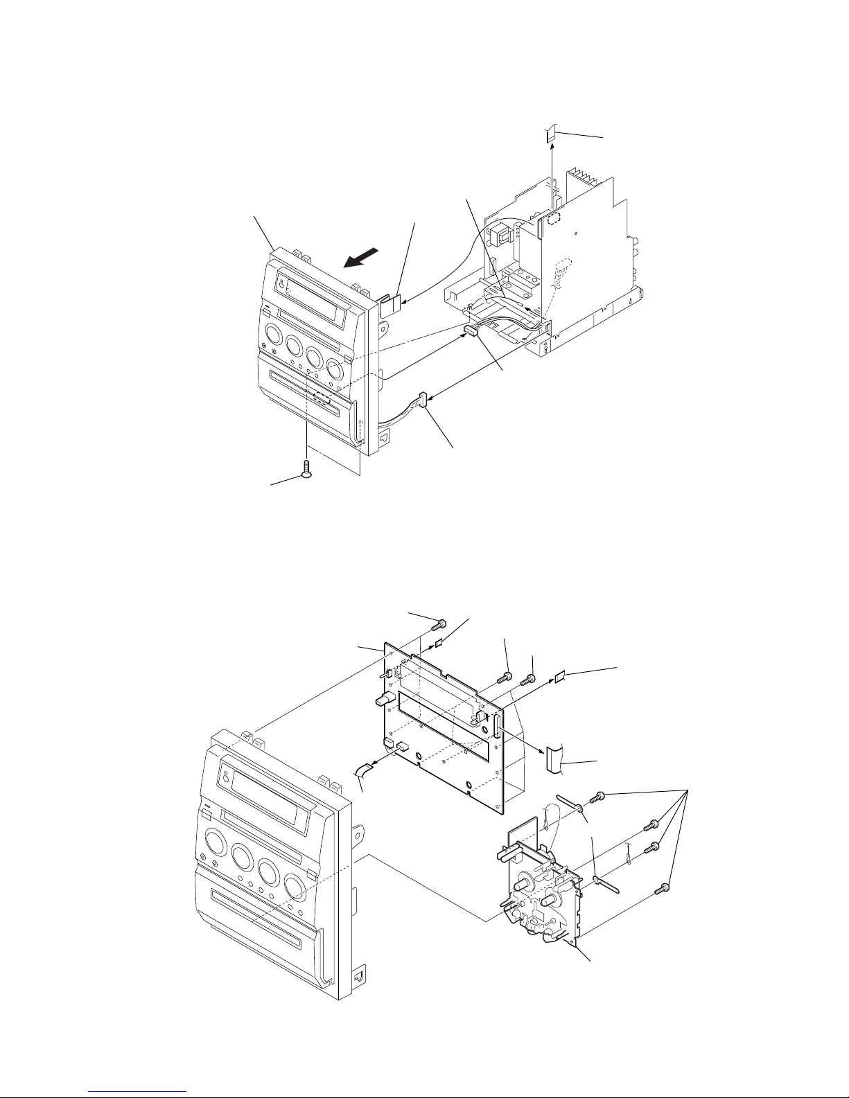
3-4. Front Panel Assy.............................................................. 9
3-5. CONTROL Board, Single Cassette Mechanism ............. 9
3-6. MAIN Board, POWER Board ......................................... 10
3-7. VCD Board,
CD Mechanism Deck (CDM55A-30BD61S).................. 11
3-8. LOADING Board ............................................................ 11
3-9. BD Board......................................................................... 12
3-10. Tray (CDM55D) .............................................................. 12
3-11. Base Unit (BU-30BD61S) ............................................... 13
4. TEST MODE ............................................................... 14
5. MECHANICAL ADJUSTMENTS......................... 15
6. ELECTRICAL ADJUSTMENTS .......................... 16
7. DIAGRAMS ................................................................. 19
7-1. Block Diagram
– BD Section – ................................................................ 20
– VCD Section –.............................................................. 21
– MAIN Section – ........................................................... 22
7-2. Printed Wiring Board – BD Section – ............................ 23
7-3. Schematic Diagram – BD Section – ............................... 24
7-4. Printed Wiring Board – VCD Section – ......................... 25
7-5. Schematic Diagram – VCD Section (1/2) – ................... 26
7-6. Schematic Diagram – VCD Section (2/2) – ................... 27
7-7. Printed Wiring Board – MAIN Section – ....................... 28
7-8. Schematic Diagram – MAIN Section –.......................... 29
7-9. Printed Wiring Boards – CONTROL Section – ............. 30
7-10. Schematic Diagram – CONTROL Section –.................. 31
7-11. Printed Wiring Boards
– MIC ECHO/PHONE Section – .................................... 32
7-12. Schematic Diagram – MIC ECHO/PHONE Section – .. 33
7-13. Printed Wiring Board – POWER Section –.................... 34
7-14. Schematic Diagram – POWER Section – ...................... 35
8. EXPLODEDVIEWS
8-1. Overall Section ................................................................ 41
8-2. Front Section ................................................................... 42
8-3. Chassis Section................................................................ 43
8-4. CD Mechanism Deck Section ......................................... 44
8-5. Base Unit Section ............................................................ 45
9. ELECTRICAL PARTS LIST .................................. 46

3
HCD-GP6V
Notes on chip component replacement
•Never reuse a disconnected chip component.
•Notice that the minus side of a tantalum capacitor may be
damaged by heat.
Flexible Circuit Board Repairing
•Keep the temperature of the soldering iron around 270 °C
during repairing.
•Do not touch the soldering iron on the same conductor of the
circuit board (within 3 times).
•Be careful not to apply force on the conductor when soldering
or unsoldering.
SAFETY-RELATED COMPONENT WARNING!!
COMPONENTS IDENTIFIED BY MARK 0OR DOTTED LINE
WITH MARK 0ON THE SCHEMATIC DIAGRAMS AND IN
THE PARTS LIST ARE CRITICAL TO SAFE OPERATION.
REPLACE THESE COMPONENTS WITH SONY PARTS WHOSE
PART NUMBERS APPEAR AS SHOWN IN THIS MANUAL OR
IN SUPPLEMENTS PUBLISHED BY SONY.
CAUTION
Use of controls or adjustments or performance of procedures
otherthan those specifiedherein mayresult inhazardousradiation
exposure.
UNLEADED SOLDER
Boards requiring use of unleaded solder are printed with the lead-
free mark (LF) indicating the solder contains no lead.
(Caution: Some printed circuit boards may not come printed with
the lead free mark due to their particular size)
: LEAD FREE MARK
Unleaded solder has the following characteristics.
•Unleaded solder melts at a temperature about 40 °C higher
than ordinary solder.
Ordinary soldering irons can be used but the iron tip has to be
applied to the solder joint for a slightly longer time.
Soldering irons using a temperature regulator should be set to
about 350 °C.
Caution: The printed pattern (copper foil) may peel away if
the heated tip is applied for too long, so be careful!
•Strong viscosity
Unleaded solder is more viscou-s (sticky, less prone to flow)
than ordinary solder so use caution not to let solder bridges
occur such as on IC pins, etc.
•Usable with ordinary solder
It is best to use only unleaded solder but unleaded solder may
also be added to ordinary solder.
SECTION 1
SERVICING NOTES
This appliance is classified as a CLASS 1 LASER product.
The CLASS 1 LASER PRODUCT MARKING is located on the
exterior.
Laser component in this product is capable of emitting radiation
exceeding the limit for Class 1.
The laser diode in the optical pick-up block may suffer electrostatic
break-down because of the potential difference generated by the
charged electrostatic load, etc. on clothing and the human body.
During repair, pay attention to electrostatic break-down and also
use the procedure in the printed matter which is included in the
repair parts.
The flexible board is easily damaged and should be handled with
care.
NOTES ON LASER DIODE EMISSION CHECK
The laser beam on this model is concentrated so as to be focused on
the disc reflective surface by the objective lens in the optical pick-
up block. Therefore, when checking the laser diode emission,
observe from more than 30 cm away from the objective lens.
LASER DIODE AND FOCUS SEARCH OPERATION
CHECK
Carry out the “S curve check” in “CD section adjustment”and check
that the S curve waveforms is output three times.
NOTES ON HANDLING THE OPTICAL PICK-UP
BLOCK OR BASE UNIT

4
HCD-GP6V
Service Position of the CD Mechanism Deck andVCD Board
Service Position of theTape Cassette Mechanism Deck
CD Mechanism Dec
k
(CDM55A-30BD61S)
VCD Board
CN806
MAIN Board
CN802
Extension cable J-2501-245-A
(1.00mm/23P/L300)
Extension cable J-2501-225-A
(1.00mm/9P/L300)
MAIN Board
Tape Cassette Mechanism Deck
(CMAL1Z240A)

5
HCD-GP6V
SECTION 2
GENERAL This section is extracted
from instruction manual.
Main unit
Cassette compartment qg
CD SYNC qd (18)
DIRECTION 9(17, 18, 22)
Disc tray 4
Display window 3
MD qk (26)
MIC/ECHO qa (19)
MIC jack qh
PHONES jack qj
PLAY MODE/TUNING MODE
9(9, 12, 14, 16)
Remote sensor 2
REPEAT/FM MODE 8(12, 16)
TUNER/BAND qk (14, 16)
TUNING +/– 6(14, 16)
VOLUME +/– 7(19, 21)
?/1 (power) 1(7, 8, 15, 21, 22)
.m/M> (go back/go
forward or fast forward/
rewind) 6(8, 10, 12, 13, 17,
18, 19, 21, 22, 24)
x(stop) qs (10, 11, 13, 15, 17,
18, 20, 29)
zREC PAUSE/START qf (18,
20)
CD NX (play/pause) ql (9, 11,
12, 15, 33)
TAPE nN (play) ql (17, 18)
Z(CD open/close) 5(9, 10)
Z PUSH (tape open/close) 0
(17)
List of button locations and reference pages
How to use this page
Use this page to find the location of buttons and other
parts of the system that are mentioned in the text.
Ill
us
t
ra
ti
on num
b
er
r
DISPLAY 2(16, 24)
RR
Name of button/part Reference page
ALPHABETICAL ORDER
A – M P – Z
BUTTON DESCRIPTIONS
12 345
6
7
8
ql
qk
qj
qh 9
0q
a
q
s
q
d
q
f
q
g

6
HCD-GP6V
Remote control
ALBUM +/– qf (10)
BASS/TREBLE wa (19)
CD wf (9, 12, 15)
CLEAR qk (13, 15)
CLOCK/TIMER SELECT w;
(22, 23)
CLOCK/TIMER SET 4(8, 21,
22)
DISPLAY 2(16, 24)
DSG qd (19)
ENTER 3(8, 12, 15, 21, 22)
KEY CONTROL 7(20)
K.PON/MPX ql (19)
NEXT 9(11)
Numeric buttons 6(10, 11, 13,
16)
ON SCREEN wj (25)
PICTURE EFFECT* wh
PREV 9(11)
SELECT q;
SLEEP qj (21)
SPECIAL MENU qh (13)
TAPE wd (17)
TUNER BAND ws (14, 16)
TUNING MEMORY 5(14)
VOLUME +/– qs (19, 21)
?/1 (power) 1(7, 8, 15, 21, 22)
m/M (fast forward/rewind)
8(10, 13, 17)
./> (go back/go forward)
9(8, 10, 12, 18, 19, 21, 22,
24)
x(stop) qa (10, 11, 13, 15, 17,
18, 20, 29)
X(pause) qg (10, 17)
N(play) q; (9, 11, 12, 17, 18,
33)
+/– 9
RETURN Owg (11)
*This button cannot be used in
this system.
ALPHABETICAL ORDER
A – K N – Z
BUTTON DESCRIPTIONS
`/1
X
O
1
3
2
qj
qk
qh
4
5
6
8
7
qs
qf
0
qa
qg
qd
9
`/1
X
O
w;
ql
wa
ws
wd
wf
wj
wg
wh
Use buttons on the remote for the operation.
1
Press ?/1 to turn on the system.
2
Press CLOCK/TIMER SET.
3
Press ./> repeatedly to set the
hour.
4
Press ENTER.
5
Press ./> repeatedly to set the
minute.
6
Press ENTER.
The clock starts working.
To adjust the clock
1Press CLOCK/TIMER SET.
2Press ./> to select “CLOCK”, then
press ENTER.
3Do the same procedures as step 3 to 6
above.
Setting the clock

7
HCD-GP6V
SECTION 3
DISASSEMBLY
•This set can be disassembled in the order shown below.
3-6.MAIN BOARD,
POWER BOARD
(Page 10)
3-8.LOADING BOARD
(Page 11) 3-9.BD BOARD
(Page 12) 3-10.TRAY (CDM55D)
(Page 12)
3-11.BASE UNIT
(BU-30BD61S)
(Page 13)
3-7.VCD BOARD,
CD MECHANISM DECK
(CDM55A-30BD61S)
(Page 11)
3-5.CONTROL BOARD,
SINGLE CASSETTE MECHANISM
(Page 9)
3-4.FRONT PANEL ASSY
(Page 9)
3-3.CD MECHANISM SECTION
(Page 8)
3-2.MIC/ECHO BOARD
(Page 8)
SET
3-1.TOP CABINET,
V-OUT BOARD, DC FAN
(Page 7)
7
two screws
(+BVTP 3
×
10)
qh
two screws
(+BVTP 3
×
10)
qd
screw
(+BVTP 3
×
10)
qs
screw (+BVWH 3
×
10)
6
three screws
(+BVTP 3
×
10)
4
qk
rear panel
qj
DC fan
q;
tuner (FM/AM)
9
wire (flat type)
11p
a
a
b
b
5
top cabinet
1
three screws
(+KTP 3
×
12)
2
three screws
(+KTP 3
×
12)
3
six screws
(+BVTP 3
×
10)
8
three screws
(+BVTP 3
×
10)
qa
connector 4p
(CN202)
qf
V-OUT board
qg
connector 2p
(CN401)
Note: Follow the disassembly procedure in the numerical order given.
3-1. TOP CABINET,V-OUT BOARD, DC FAN

8
HCD-GP6V
3-2. MIC/ECHO BOARD
3-3. CD MECHANISM SECTION
3
two screws
(+BVTP 3
×
10)
1
connector 4p
(CN501)
4
MIC/ECHO board
2
wire (flat type) 6p (CN502
)
6
four screws
(+BVTP 3
×
10)
3
screw (+BVTP 3
×
10)
8
wire (flat type) 5p (CN801
)
q;
CD mechanism section
7
4
wire (flat type) 11p (CN303)
5
wire 1p (CLP401)
9
connector 5p (CN1)
1
four claws
2
CD lid

9
HCD-GP6V
3-4. FRONT PANEL ASSY
3-5. CONTROL BOARD, SINGLE CASSETTE MECHANISM
1
two screws
(+KTP 3
×
12)
3
wire (flat type) 21p (CN302)
4
8
front panel assy
5
connector 6p
6
connector 5p (CN201)
2
wire (flat type) 6p (CN305
)
7
wire 1p (CLP201)
qa
single cassette mechanism
(CMAL1Z240A)
8
CONTROL board
1
four screws (+BVTP 3
×
10)
2
four screws (+BVTP 3
×
10)
3
five screws (+BVTP 3
×
10)
9
four screws
(+BVTP 3
×
10
)
6
wire (flat type) 21p (CN601)
4
wire (flat type) 5p (CN602)
5
wire (flat type) 6p (CN605)
7
wire (flat type)
8p (CN603)
q;
two clamp

10
HCD-GP6V
3-6. MAIN BOARD, POWER BOARD
qa
four screws
(+B 4
×
8)
8
heat sink assy
1
connector 11p (CN801)
a
a
q;
MAIN board
2
two screws (+BVTP 3
×
10)
3
screw (+BVTP 3
×
10)
4
holder heat sink
qs
silicon shield plate
6
two screws
(+BTP 2.6
×
8)
5
two screws
(+BVTP 3
×
10)
7
two screws
(+BVTP 3
×
10
)
qd
TRANSFORMER
board
qf
power transformer
9
wire (flat type)
6p (CN306)

11
HCD-GP6V
3-7. VCD BOARD, CD MECHANISM DECK (CDM55A-30BD61S)
qd
screw (+BVTP 3
×
10)
qa
two screws (+BVTP 3
×
10)
qs
holder, shield case
8
two screws (+BVTP 3
×
10)
q;
two screws (+BVTP 3
×
10)
9
VCD board
qf
CD holder
2
two screws (+BVTP 3
×
10)
qh
CD mechanism
deck
4
lid (VCD), shield case
3
wire assy
6
wire (flat type) 23p (CN802
)
1
wire (flat type) 9p (CN803)
7
wire (flat type) 11p (CN806)
5
connector
4p (CN804)
qg
CD plate
5
LOADING board
2
two screws (+BTP 2.6
×
6)
4
motor (LD) assy
(M901)
1
Remove the belt.
3
Remove soldering from the two points.
3-8. LOADING BOARD

12
HCD-GP6V
3-9. BD BOARD
2
Remove soldering
from the four points.
5
BD board
1
wire (flat type) 25p (CN103)
4
wire (flat type) 16
p
3
claw
2
tray
1
While pressing the two protrusions
A
and
B
to unlock the two claws as shown,
pull the tray in the direction of the arrow
C
. (Be careful of the claws.)
claw
claw
C
A
B
3-10. TRAY (CDM55D)

13
HCD-GP6V
4
two floating screw
s
(+PTPWH M2.6)
3
two floating screws
(+PTPWH M2.6)
1
floating screws
(+PTPWH M2.6)
2
5
BU holder (BU-30)
7
two insulators
6
two insulators
base unit
(BU-30BD61S)
8
wire (flat type) 9p (CN105)
3-11. BASE UNIT (BU-30BD61S)

14
HCD-GP6V
[Cold Reset]
•The cold reset clears all data including preset data stored in
the RAM to initial conditions. Execute this mode when re-
turning the set to the customer.
Procedure:
1. Press the "/1button to turn off the main power.
2. While depressing the x button, press the "/1button.
3. The fluorescent indicator tube does not display any message
and the set is reset.
[Fluorescent IndicatorTube Test Mode]
•Fluorescent segments are tested when this test is activated.
Procedure:
1. Extract an AC plug.
2. While depressing the CD ubutton, insert an AC plug.
3. All segments of the fluorescent indicator tube turn on.
4. CD test mode is activated.
5. To exit from this mode, press the "/1button or disconnect the
power cord.
[Version Display Mode]
•The model and the version are displayed.
Procedure:
1. Press the "/1button to turn the set on.
2. To enter the test mode, press two buttons x and "/1simulta-
neously for more than five seconds. The model and the ver-
sion are displayed.
[AMPTest]
•This mode is used to check the function of the amplifier.
Procedure:
1. Extract an AC plug.
2. While depressing the [MD] button, insert an AC plug to enter
the AMP test mode. The message “AMP TEST” is displayed.
3. The message “Volume MAX” is displayed, when pressing the
[VOLUME +] button. The message “Volume MIN” is displayed,
when pressing the [VOLUME --] button.
4. Each time pressing the [PLAY MODE/TUNING MODE] button,
the message “EQ MAX”, “EQ MIN” or “EQ FLAT” is dis-
played in this order.
5. To release from this mode, disconnect the AC plug and turn
the power off.
[AM Channel Step 9 kHz/10kHz Selection Mode]
•Either the 9 kHz step or 10 kHz step can be selected for the
AM channel step.
Procedure:
1. Set the function to AM.
2. While depressing the [TUNER/BAND] button, press the "/1
button.
3. The channel step is changed over.
[TCTest Mode]
Procedure:
1. Extract an AC plug.
2. While depressing the TAPE nN button, insert anAC plug.
3. The message “TC TEST” is displayed and TC test mode is
activated.
•Zero Return
1. Press the + > M or – .m button.
2. The tape is rewound to the counter zero position.
•Automatic record/playback test
1. Press the [REC START/REC PAUSE] button.
2. The message “MD” is displayed and AUX input is selected.
3. The tape is rewound to the counter zero position and record-
ing is started automatically.
4. When the x button is pressed, the tape is rewound to the
recording stated point and the set starts playback.
5. To exit from this mode, press the "/1button or disconnect the
power cord.
SECTION 4
TEST MODE

15
HCD-GP6V
SECTION 5
MECHANICAL ADJUSTMENTS
3.04 – 6.96 mN • m
(31 to 71 g • cm)
(0.43 – 0.98 oz • inch)
0.20 – 0.58 mN • m
(2 to 6 g • cm)
(0.02 – 0.08 oz • inch)
3.04 – 6.96 mN • m
(31 to 71 g • cm)
(0.43 – 0.98 oz • inch)
0.20 – 0.58 mN • m
(2 to 6 g • cm)
(0.02 – 0.08 oz • inch)
6.97 – 14.02 mN • m
(71 to 143 g • cm)
(0.98 – 1.99 oz • inch)
9.8 mN • m or more
(100 g • cm or more)
(1.4 oz • inch or more)
9.8 mN • m or more
(100 g • cm or more)
(1.4 oz • inch or more)
CQ-102C
CQ-102C
CQ-102RC
CQ-102RC
CQ-201B
CQ-403A
CQ-403R
Precaution
1. Clean the following parts with a denatured alcohol-moistened
swab:
record/playback heads pinch rollers
erase head rubber belts
capstan idlers
2. Demagnetize the record/playback head with a head demag-
netizer.
3. Do not use a magnetized screwdriver for the adjustments.
4. After the adjustments, apply suitable locking compound to the
parts adjusted.
5. The adjustments should be performed with the rated power
supply voltage unless otherwise noted.
Torque Measurement
Mode
FWD
FWD
back tension
REV
REV
back tension
FF/REW
FWD tension
REV tension
Torque meter Meter reading

16
HCD-GP6V SECTION 6
ELECTRICAL ADJUSTMENTS
[Record/Playback Head Azimuth Adjustment]
Procedure:
1. Mode : Playback
2. Turn the adjustment screw and check output peaks. If the peaks
do not match for L-CH and R-CH, turn the adjustment screw
so that outputs match within 1 dB of peak.
test tape
P-4-A100
(10kHz, –10dB) MAIN board
J203
speaker terminal
level meter
set +
–
L-CH
peak
R-CH
peak
screw
position
output
level within
1 dB
L-CH
peak R-CH
peak
screw
position
within 1dB
Signal Used forTape
P-4-A100
WS-48B
10 kHz, –10 dB
3 kHz, 0 dB
Azimuth Adjustment
Tape Speed Adjustment
DECK SECTION 0 dB=0.775V
1. Demagnetizethe record/playbackheadwithaheaddemagnetizer.
2. Do not use a magnetized screwdriver for the adjustments.
3. After the adjustments, apply suitable locking compound to the
parts adjusted.
4. The adjustments should be performed with the rated power
supply voltage unless otherwise noted.
5. The adjustments should be performed in the order given in this
service manual. (As a general rule, playback circuit adjustment
should be completed before performing recording circuit
adjustment.)
6. The adjustments should be performed for both L-CH and R-
CH.
7. Switches and controls should be set as follows unless otherwise
specified.
4. After the adjustments, apply suitable locking compound to the
parts adjusted.
Adjustment Location:Record/Playback/Erase Head
[Tape Speed Check]
Procedure:
1. Turn the power on.
2. Insert the WS-48B into deck.
3. Press the Ybutton of deck.
4. Check the reading of frequency counter becomes 3000 ± 90 Hz.
Sample Value of Wow and flutter
W.RMS (JIS) less than 0.3%
(test tape: WS-48B)
3. Mode: Playback
test tape
P-4-A100
(10kHz, –10dB) oscilloscope
set
Waveform of oscilloscope
in phase 45
°
90
°
135
°
180
°
good wrong
MAIN board
J203
speaker terminal
L
R

17
HCD-GP6V
RFDC signal waveform
Checking Location: BD board (Conductor side)
RFAC Level Check
Connection:
Procedure:
1. Connect an oscilloscope to test point TP6 (RFAC) and TP7
(VC) on the BD board.
2. Turn the power on.
3. Put the disc (YEDS-18) in to playback the number five track.
4. Confirm that oscilloscope waveform is clear and check RFAC
signal level is correct or not.
Note: A clear RFAC signal waveform means that the shape “◊” can be
clearly distinguished at the center of the waveform.
RFAC signal waveform
Checking Location: BD board (Conductor side)
CD SECTION
Note:
1. CD Block is basically designed to operate without adjustment. There-
fore, check each item in order given.
2. UseYEDS-18 disc (3-702-101-01) unless otherwise indicated.
3. Use an oscilloscope with more than 10MΩimpedance.
4. Clean the object lens by an applicator with neutral detergent when the
signal level is low than specified value with the following checks.
S-curve Check
Connection:
Procedure:
1. Connect an oscilloscope to test point TP4 (FE) and TP7 (VC)
on the BD board.
2. Turn the power on.
3. Put the disc (YEDS-18) in and turned power switch on again
and actuate the focus search. (actuate the focus search when
disc table is moving in and out)
4. Check the oscilloscope waveform (S-curve) is symmetrical
betweenA and B.And confirm peak to peak level within 2 ± 1
Vp-p.
S-curve waveform
Note: •Try to measure several times to make sure than the ratio of A : B
or B : A is more than 10 : 7.
•Take sweep time as long as possible and light up the
brightness to obtain best waveform.
Checking Location: BD board (Conductor side)
RFDC Level Check
Connection:
Procedure:
1. Connect an oscilloscope to test point TP6 (RFDC) and TP7
(VC) on the BD board.
2. Turn the power on.
3. Put the disc (YEDS-18) in to playback the number five track.
4. Confirm that oscilloscope waveform is clear and check RFDC
signal level is correct or not.
Note: A clear RFDC signal waveform means that the shape “◊” can be
clearly distinguished at the center of the waveform.
+
–
BD board
TP4 (FE)
TP7 (VC)
oscilloscope
A
B
symmetry
within 2
±
1 Vp-p
+
–
BD board
TP6 (RFDC)
TP7 (VC)
oscilloscope
VOLT/DIV: 200 mV
TIME/DIV: 500 ns
level: 0.7
±
0.2 Vp-p
+
–
BD board
TP6 (RFAC)
TP7 (VC)
oscilloscope
VOLT/DIV: 200 mV
TIME/DIV: 500 ns
level: 1.0
±
0.4 Vp-p

18
HCD-GP6V
Connecting Location:
– BD BOARD (Conductor Side) –
IC101
TP7
(VC)
IC103
TP8
(RFAC)
TP6
(RFDC)
TP4
(FE)
TP2
(TE)
Ver 1.1

1919
HCD-GP6V
SECTION 7
DIAGRAMS
•Circuit Boards Location
For Schematic Diagrams.
Note:
•All capacitors are in µF unless otherwise noted. (p: pF)
50 WV or less are not indicated except for electrolytics and
tantalums.
•All resistors are in Ωand 1/4W or less unless otherwise
specified.
• f: internal component.
•5: fusible resistor.
•C: panel designation.
•A: B+ Line.
•H: adjustment for repair.
•Voltages and waveforms are dc with respect to ground un-
der no-signal (detuned) conditions.
no mark: CD PLAY
( ):TAPE REC
•Voltages are taken with aVOM (Input impedance 10 MΩ).
Voltage variations may be noted due to normal production
tolerances.
•Waveforms are taken with a oscilloscope.
Voltage variations may be noted due to normal production
tolerances.
•Circled numbers refer to waveforms.
•Signal path.
F: TUNER (FM/AM)
J: CD PLAY
E: TAPE PLAY
a: REC
j: AUX (VIDEO) IN
L: VIDEO OUT
•Abbreviation
EA : Saudi Arabia model
MY : Malaysia model
SP : Singapore model
For Printed Wiring Boards.
Note:
•X: parts extracted from the component side.
•Y: parts extracted from the conductor side.
•W : indicates side identified with part number.
• f: internal component.
•: Pattern from the side which enables seeing.
(The other layers' patterns are not indicated.)
THIS NOTE IS COMMON FOR PRINTEDWIRING BOARDS AND SCHEMATIC DIAGRAMS.
(In addition to this, the necessary note is printed in each block.)
Note: The components identified by mark 0or dotted
line with mark 0are critical for safety.
Replace only with part number specified.
Caution:
Pattern face side:Parts on the pattern face side seen from
(Side B) the pattern face are indicated.
Parts face side: Parts on the parts face side seen from
(Side A) the parts face are indicated.
•Indication of transistor.
C
BThese are omitted.
E
Q
B
These are omitted.
CE
Q
B
These are omitted.
CE
Q
MAIN board
BD board
LOADING board
CONTROL board
PHONE board
V-OUT BOARD
MIC/ECHO BOARD
VCD BOARD
POWER BOARD
1.0
±
0.4Vp-p
Approx. 360mVp-p
Approx. 1.2Vp-p
0.6
±
0.15Vp-p
3.7Vp-p
59.1ns
4.6Vp-p
37 ns
5.5Vp-p
30.6
µ
s
2.4Vp-p
115ns
•Waveforms
– BD Board – –VCD Board –
11.7Vp-p
11.7
µ
s
1IC103 qg (RFAC)
(CD play mode)
200 mV/DIV 1
µ
s/DIV
2IC101 qh (FE)
(CD play mode)
100 mV/DIV 200
µ
s/DIV
6IC802 ua (XOUT)
1 V/DIV 10 ns/DIV
7Q301 collector
(REC mode)
2 V/DIV 5
µ
s/DIV
8IC601 qd (O-XT2)
1 V/DIV 10
µ
s/DIV
9IC601 qh (XOUT)
1 V/DIV 50 ns/DIV
4IC103 wk (RFDC)
(CD play mode)
5IC101 us (XTAO)
100 mV/DIV 1
µ
s/DIV
1 V/DIV 20 ns/DIV
3IC101 qk (TE)
(CD play mode)
500 mV/DIV 200
µ
s/DIV
– CONTROL Board –
– MAIN Board –

2020
HCD-GP6V
7-1. BLOCK DIAGRAM — BD SECTION —
: CD
• Signal Path
OPTICAL PICK-UP
BLOCK
PD1
PD2
I5-10
I1-6
LD
VC
VCC
7
5
3
1
2
4+3.3V
GND
IL-SW
PD
VR
LD
DRIVE
FOCUS
COIL
TRACKING
COIL
Q101
RF AMP
IC103
VC
27
A
6
B
7
C
8
D
9
E
10
F
11
LD
1
PD
2
IC102
MOTOR/COIL DRIVE
VO1+
52
VO1-
47
VO2+
56
VO2-
55
VO3+
2
VO3-
1
M
(SLED)
M102
M101 VO4+
10
VO4-
5
M
(SPINDLE)
F+
F-
T+
T-
35
IN1+
34
IN1-
32
IN2+
31
IN2-
27
IN3+
26
IN3-
24
IN4R
8
STBY
MDP
25
SRDR
30
SFDR
29
TRDR
32
TFDR
31
FRDR
34
FFDR
33
DIGITAL SIGNAL PROC.
IC101
DIGITAL SERVO
RFAC
50
29
RFDCI
28
RFDC
16
FE
17
FEI
12
SWTE_BAL
RFDC
43
FE
39
TE
41
SE
40
SSTP
26
66
PCMD
4
DATA
16.9344MHz
6
CLOK
5
XLAT
DATA
XLAT
77
SQCK SQCK
8
SCLK
15
SCOR
76
SQSO
2
XRST
XRST
RF-SW
PWM3
PWM2
PWM1
7
SENS
SCOR
SQSO
SENS
14
C2PO C2PO
15
RF AC
18
TE
67
BCLK
65
LRCK
13
GFS
22
FOK
PCMD
CLK
BCLK
LRCK
GFS
FOK
71
XTAI
72
XTAO
19
RV101
X201
AVDD(3.3V)
AVCD
SECTION
BVCD
SECTION
CVCD
SECTION
Table of contents
Other Sony Stereo System manuals

Sony
Sony HCD-H5 User manual

Sony
Sony HCD-CP33 User manual

Sony
Sony HCD-CPZ1DAB User manual

Sony
Sony HCD-GX25 - System Components User manual

Sony
Sony MEX-GS820BT User manual

Sony
Sony HCD-VR90AV User manual

Sony
Sony ZS-X1 - Cd Boombox User manual

Sony
Sony HCD-PX333 User manual

Sony
Sony LBT-D670AV - Compact Hifi Stereo System User manual

Sony
Sony SRS-BTX500 User manual

Sony
Sony HCD-H66 User manual

Sony
Sony MHC-GT4D User manual

Sony
Sony CMT-CP333 - Micro Hi Fi Component System Setup guide

Sony
Sony HCD-H1200 User manual

Sony
Sony MHC-M20D Quick start guide

Sony
Sony LBT-DR7AV User manual

Sony
Sony LBT-LX5 User manual

Sony
Sony SRS-X33 Reference guide

Sony
Sony MHC-DX20 User manual

Sony
Sony ZS-BTY50 User manual