Sony HCD-RXD2 User manual

HCD-RXD2
US Model
SERVICE MANUAL
MINI Hi-Fi COMPONENT SYSTEM
MICROFILM
SPECIFICATIONS
HCD-RXD2 is the tuner, deck, CD and
amplifiersectioninMHC-RXD2.
Model Name Using Similar Mechanism HCD-G101
CD Mechanism Type CX3
Base Unit Type KSM-213ECM
Optical Pick-up Type KSS-213ECM/C2NP
Model Name Using Similar Mechanism NEW
Tape Transport Mechanism Type CWL-44-FF
CD
SECTION
TAPE
DECK
SECTION

— 2 —
After correcting the original service problem, perform the following
safety checks before releasing the set to the customer:
Checktheantennaterminals, metaltrim, “metallized”knobs, screws,
and all other exposed metal parts forAC leakage. Check leakage as
described below.
LEAKAGE
The AC leakage from any exposed metal part to earth ground and
from all exposed metal parts to any exposed metal part having a
return to chassis, must not exceed 0.5 mA (500 microamperes).
Leakage current can be measured by any one of three methods.
1. A commercial leakage tester, such as the Simpson 229 or RCA
WT-540A. Follow the manufacturers’instructions to use these
instruments.
2. A battery-operated AC milliammeter. The Data Precision 245
digital multimeter is suitable for this job.
3. Measuring the voltage drop across a resistor by means of a
VOM or battery-operatedAC voltmeter.The “limit” indication
is 0.75 V, so analog meters must have an accurate low-voltage
scale. The Simpson 250 and Sanwa SH-63Trd are examples of
a passive VOM that is suitable. Nearly all battery operated
digital multimeters that have a 2VAC range are suitable. (See
Fig. A)
SAFETY CHECK-OUT
To Exposed Metal
Parts on Set
0.15
µ
F1.5 k
Ω
AC
Voltmeter
(0.75 V)
Earth Ground
Fig.A. Using anAC voltmeter to checkAC leakage.
This appliance is classified as a CLASS 1 LASER product. The
CLASS 1 LASER PRODUCT MARKING is located on the rear
exterior.
Laser component in this product is capable of emitting radiation
exceeding the limit for Class 1.
CAUTION
Use of controls or adjustments or performance of procedures
otherthan thosespecified hereinmay resultin hazardousradiation
exposure.
SAFETY-RELATED COMPONENT WARNING!!
COMPONENTS IDENTIFIED BY MARK !OR DOTTED LINEWITH
MARK !ON THE SCHEMATIC DIAGRAMS AND IN THE PARTS
LIST ARE CRITICAL TO SAFE OPERATION. REPLACE THESE
COMPONENTS WITH SONY PARTS WHOSE PART NUMBERS
APPEAR AS SHOWN IN THIS MANUAL OR IN SUPPLEMENTS
PUBLISHED BY SONY.

— 3 —
TABLE OF CONTENTS
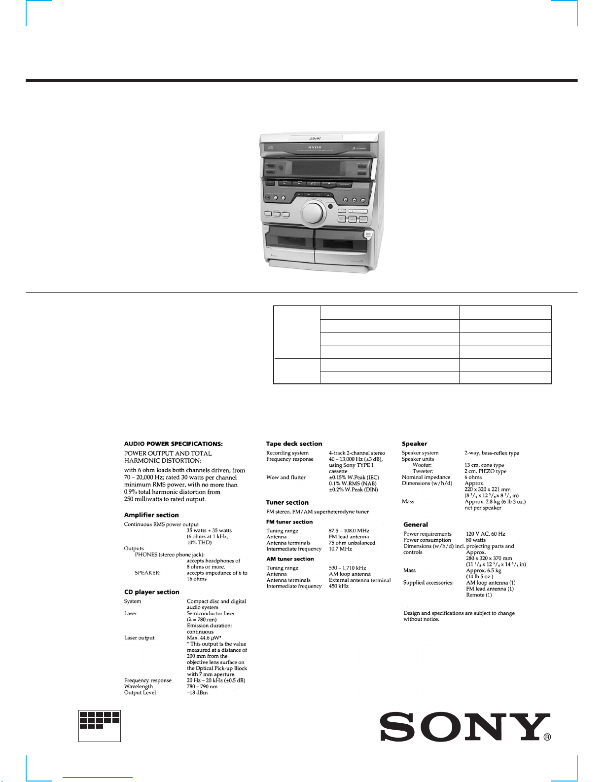
1. GENERAL ·········································································· 4
2. DISASSEMBLY
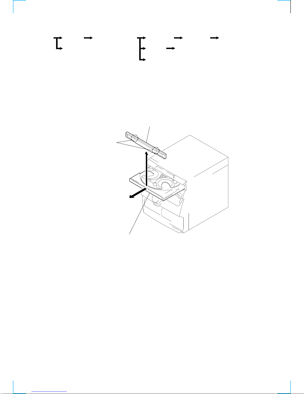
2-1. CD Door ············································································· 5
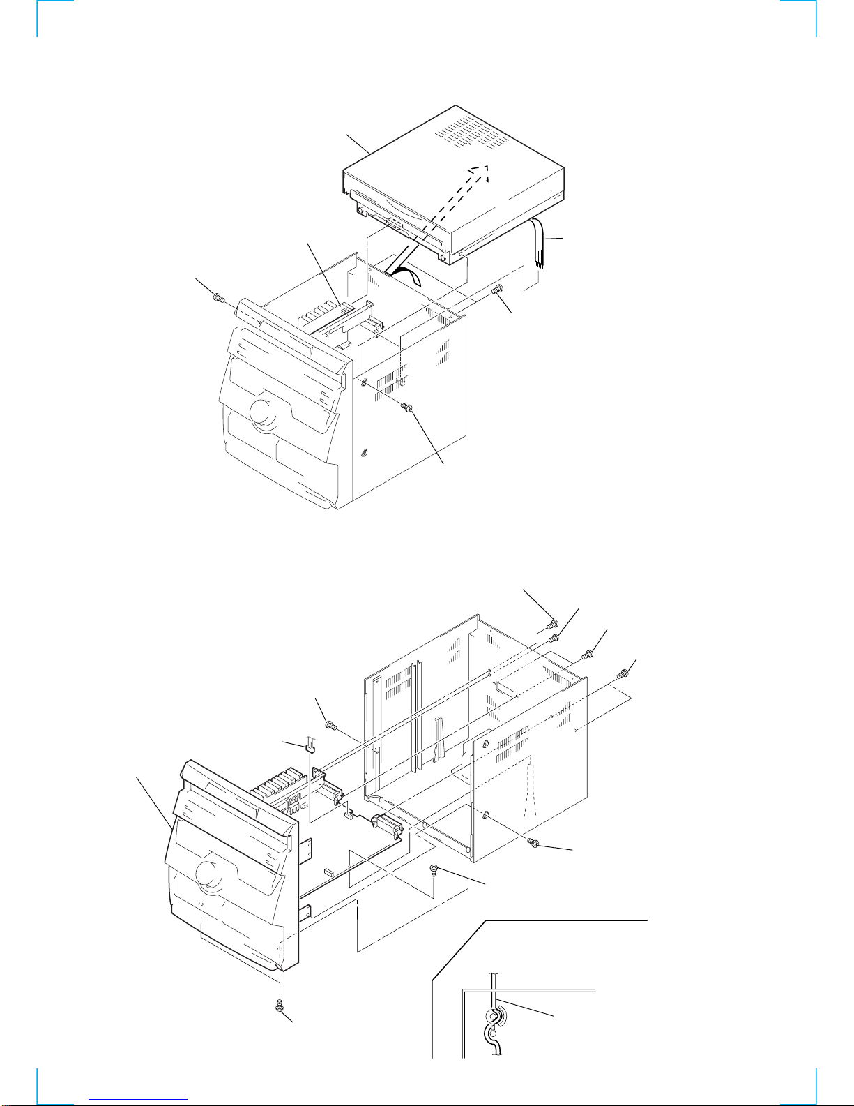
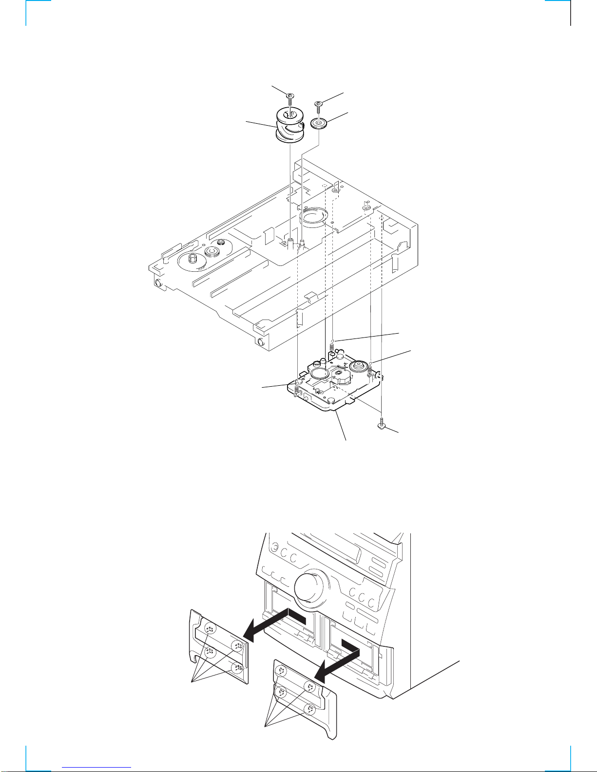
2-2. CD Mechanism Deck ························································· 6
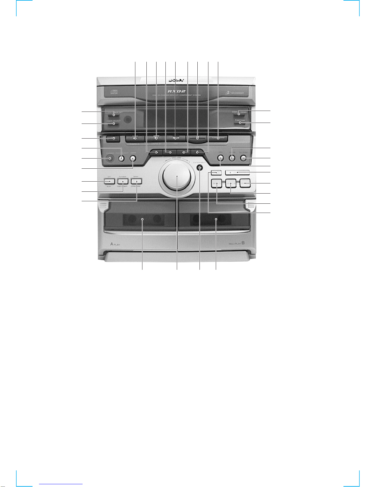
2-3. Front Panel ········································································· 6
2-4. Main Board········································································· 7
2-5. Front Board········································································· 7
2-6. CD Tray ·············································································· 8
2-7. CD Decord Board ······························································· 8
2-8. Base Unit ············································································ 9
2-9. Cassette Lid (L) / (R)·························································· 9
3. TEST MODE···································································· 10
4. MECHANICAL ADJUSTMENTS ····························· 11
5. ELECTRICAL ADJUSTMENTS ······························· 11
6. DIAGRAMS
6-1. Circuit Boards Location ··················································· 16
6-2. Block Diagrams ································································ 17
•Tuner, CD Section ························································· 17
•Main Section·································································· 19
6-3. Printed Wiring Board – CD Decoder Section – ··············· 23
6-4. Schematic Diagram – CD Decoder Section – ·················· 25
6-5. Printed Wiring Board – Front Section – ··························· 27
6-6. Schematic Diagram – Front Section –······························ 29
6-7. Printed Wiring Board – Main Section – ··························· 31
6-8. Schematic Diagram –Main (1/4) Section – ······················ 33
6-9. Schematic Diagram – Main (2/4) Section – ····················· 35
6-10. Schematic Diagram – Main (3/4) Section – ····················· 37
6-11. Schematic Diagram – Main (4/4) Section – ····················· 39
6-12. IC Pin Function ································································ 41
6-13. IC Block Diagrams ··························································· 43
7. EXPLODEDVIEWS
7-1. Cabinet Section································································· 47
7-2. Front Panel Section ·························································· 48
7-3. CD Mechanism Deck Section-1 ······································· 49
7-4. CD Mechanism Deck Section-2 ······································· 50
7-5. Base Unit Section (KSM-213ECM)································· 51
8. ELECTRICAL PARTS LIST ······································· 52

— 4 —
SECTION 1
GENERAL
4
3
2
1
#™
#¡
#º
@ª
@•
@¶
@§ @∞ @¢ @£
@™
@¡
@º
!ª
!•
!¶
!§
!∞
!¢
!£
56789!º !¡ !™
11/u(Power) button
2TIMER SELECT button
3CLOCK/TIMER button
4TAPE A (button and indicator
5–, 0button
6TAPE B (button and indicator
7=button
8CD, ^button and indicator
9+button
!º pbutton
!¡ +, )button
!™ TUNER/BAND button
!£ DISPLAY/DEMO button
!¢ FUNCTION button
!∞ PAUSE button and indicator
!§ CD SYNC button
!¶ REC button and indicator
!• 6OPEN/CLOSE button
!ª DISC 3 button
@º DISC 2 button
@¡ DISC 1 button
@™ DISC SKIP, EX-CHANGE button
@£ Tape deck B
@¢ ENTER/NEXT button
@∞ VOLUME knob
@§ Tape deck A
@¶ REPEAT, STEREO/MONO button
@• PLAY MODE, TUNER MEMORY button
@ª EDIT, REPLAY button
#º DBFB button
#¡ PHONES jack
#™ FILE SELECT button

— 5 —
SECTION 2
DISASSEMBLY
SET CD DOOR
(Page 5) CD MECHANISM DECK
(Page 6) FRONT PANEL
(Page 6) MAIN BOARD
(Page 7) FRONT BOAR
D
(Page 7)
CASSETTE LID (L)/(R)
(Page 9) CD TRAY
(Page 8)
CD DECORD BOARD
(Page 8)
BASE UNIT
(Page 9)
Note : Follow the disassembly procedure in the numerical order given.
1
Pull out the CD tray and remove the CD door
with releasing claws into the direction of arrow.
2
CD door
Two claws
2-1. CD DOOR

— 6 —
6
CD mechanism deck
3
Two screws (+BVTP 3
×
10)
1
Screw (+PTPWH 3
×
10)
2
Screw (+PTPWH 3
×
10)
4
Flat type wire (CN09)
5
Harness (CN301
)
8
Screw
(+PTPWH 3
×
10)
3
Screw (+BVTP 3
×
10)
4
Screw (+BVTP 3
×
10)
5
Two screws (+BVTP 3
×
10)
6
Two screws
(+BVTP 3
×
10)
7
Screw (+PTPWH 3
×
10)
9
Screw (+BVTP 3
×
10)
2
Two screws
(+BVTP 3
×
10)
1
Connector (CN701)
!º
Front panel
HOW TO SET THE
POWER CORD
power cord
2-2. CD MECHANISM DECK
2-3. FRONT PANEL

— 7 —
2
Flat type wire (CN251)
1
Harness (CN502)
3
Connector (CN203)
4
Connector (CN201)
5
Connector (CN202)
7
Nylon rivet
8
MAIN boar
d
6
Two screws
(+KTP 3
×
8)
1
Five screws (BVTP3
×
10)
2
Seven screws
(BVTP3
×
10)
5
Button
(Release the two claws)
4
Front board
6
Button
(Release the two claws
)
7
Button
(Release the
three claws)
3
Harness
(CN603)
9
Button
(Release the three claws)
!¡
Button
!™
Button
(Release the
three claws)
!£
Lens (Release
the two claws)
!º
Button
(Release the claw)
8
Button
(Release the two claws)
2-4. MAIN BOARD
2-5. FRONT BOARD

— 8 —
1
Screw (+P 2.6
×
4)
2
Bracket
4
Bracket
5
Flat type wire
(CN06)
3
Screw (+P 2.6
×
4)
6
CD tray
1
Two screws (+BVTP 3
×
10)
2
Two screws (+BVTP 3
×
10)
Two claws
7
CD decord board
3
Belt
6
Flat type wire (CN06)
5
Flat type wire (CN01)
4
Connector (CN05)
!º
Connector (CN03)
8
Two screw
(+BVTP 3
×
10)
9
Sheet
Claw
Claw
2-6. CDTRAY
2-7. CD DECORD BOARD

— 9 —
1
Two screws (+KTP 3
×
8
)
2
Screw (+PTPWH 3
×
8)
3
UD-gear
4
Screw (+PTPWH 2.6
×
8)
5
UD-cam
6
Spring
7
Spring
8
Spring
9
Base unit
1
Remove the cassette lids in the direction of arrow.
Four claws
Four claws
2-8. BASE UNIT
2-9. CASSETTE LID (L) / (R)

— 10 —
SECTION 3
TEST MODE
Function Key combination Description
Initialization
STOP + POWER OFF All preset data is re-set to the initial
(default) value.
Model display
STOP + DISC 1 Mode name is displayed.
Destination display
STOP + DISC 2 Destination is displayed.
Version display
STOP + DISC 3Version number of the
microprocessor is displayed.
CD aging mode
STOP + DISC SKIP/EX-CHANGE Set discs to DISC 1 and DISC
3. The following operations are repeated when aging
starts:
1. DISC 1: TOC Read
2. Plays back the last music of the DISC 1
3. DISC 3 : TOC Read
4. Plays back the last music of the DISC 3.
5. STOP
6. Tray is open and closed.
TAPE aging mode
STOP + PLAY A Insert a commercially available cassette tape (10
min.)tothe decksA andB. Whenaging starts,each tapeis rewound
and the following
operations are repeated:
1. TAPE A: FWD PLAY for one minute
2. TAPE A: FWD STOP for one second
3. TAPE A: FWD PLAY for three minutes
4. TAPE A: FWD FF to tape end
5. TAPE B: FWD PLAY for one minute
6. TAPE B: FWD REC PAUSE for one second
7. TAPE B: FWD REC for three minutes
8. TAPE B: FWD FF to tape end
9. TAPE B: REV PLAY for one minute
10. TAPE B: REV REC PAUSE for one second
11. TAPE B: REV REC for three minutes
12. TAPE B: REV FF to tape end.
CD service mode
STOP + OPEN/CLOSEThe message “CD S - -” is displayed on the
screen. The sled is moved to the outer circumference
while the FF button is pressed. Also, the SLED is moved to the
inner
circumference while the REW button is pressed. After pressing the
PLAY
button, FOCUS is turned ON, CLV-S is set, TRACKING and SLED
servos
are turned OFF and ADDRESS 3 = 3F, 37 is set.
Display
STOP + DBFBAll displays are turned ON.
Balance adjustment value
STOP + DISPLAY/DEMO The balance adjustment value is
displayed.
Key check
STOP + FILE SELECT Function of the pressed key is displayed.

— 11 —
Precaution
1. Clean the following parts with a denatured alcohol-moistened
swab:
record/playback head pinch rollers
erase head rubber belts
capstan idlers
2. Demagnetize the record/playback head with a head
demagnetizer.
3. Do not use a magnetized screwdriver for the adjustments.
4. After the adjustments, apply suitable locking compound to the
parts adjusted.
5. The adjustments should be performed with the rated power
supply voltage unless otherwise noted.
Torque Measurement
SECTION 4
MECHANICAL ADJUSTMENTS
Meter reading
40 to 70 g • cm
(0.56 - 0.97 oz • inch)
1 to 5 g • cm
(0.01 - 0.07 oz • inch)
55 to 140 g • cm
(0.76 - 1.94 oz • inch)
Torque
FWD
FWD
back tension
FF/REW
Torque meter
CQ-102C
CQ-102C
CQ-201B
SECTION 5
ELECTRICAL ADJUSTMENTS
1. Demagnetize the record/playback head with a head
demagnetizer.
2. Do not use a magnetized screwdriver for the adjustments.
3. After the adjustments, apply suitable locking compound to the
parts adjusted.
4. The adjustments should be performed with the rated power
supply voltage unless otherwise noted.
5. The adjustments should be performed in the order given in this
service manual. (As a general rule, playback circuit adjustment
should be completed before performing recording circuit
adjustment.)
6. The adjustments should be performed for both L-CH and R-
CH.
Record/Playback Head Azimuth Adjustment
(Deck A, Deck B)
Note: Perform this adjustments for both decks.
Procedure:
1. Mode : Playback
2. Turn the adjustment screw and check output peaks. If the peaks
do not match for L-CH and R-CH, turn the adjustment screw
so that outputs match within 2 dB of peak.
DECK SECTION 0 dB=0.775V
Tape
P-4-A100
WS-48B
Signal
10 kHz, –10 dB
3 kHz, 0 dB
Used for
Azimuth Adjustment
Tape Speed Adjustment
test tape
P-4-A100
(10kHz, –10dB)
set
SPEAKER
terminal (JK501)
level meter
L-CH
peak
R-CH
peak
screw
position
output
level within
2dB
L-CH
peak R-CH
peak
screw
position
within 2dB

— 12 —
3. Mode: Playback
4. After the adjustments, apply suitable locking compound to the
parts adjusted.
Adjustment Location:
Remove the cassette lid before adjustment (See page 9)
Tape Speed Adjustment (Deck A)
Procedure:
1. Mode: Playback
2. Adjust the SFR251 so that the frequency counter reads 3,000
Hz ± 90Hz.
Adjustment Location: MAIN board
Sample Value of Wow and flutter
W. RMS (JIS) within 0.3%
(test tape: WS-48B)
[MAIN BOARD] — Component side —
test tape
P-4-A100
(10kHz, –10dB) SPEAKER
terminal (JK501)
(L-CH)
SPEAKER
terminal (JK501)
(R-CH)
oscilloscop
e
L
R
Waveform of oscilloscope
in phase 45˚ 90˚ 135˚ 180˚
good wrong
Adjustment screws
REC/PB head (deck B)
or PB head (deck A)
test tape
WS-48B
(3kHz, 0dB)
set
SPEAKER
terminal (JK501)
frequency counte
r
+
–
Tape Speed CN251
CN601
SFR251

— 13 —
TUNER SECTION 0 dB=1µV
AMTuning Voltage Adjustment
Procedure:
1. Set the reception frequency of the unit to 530 kHz.
2. Adjust L105 for 1.2 ± 0.05 V reading on the DC voltmeter.
3. Set the reception frequency of the unit to 1,710 kHz.
4. Confirm that the voltage reading on the DC voltmeter is within
8.0 ± 0.5 V.
Adjustment Location: MAIN board (See page 14)
AMTracking Adjustment
Procedure:
1. Tune the set to 600 kHz.
2. Set the output of AM RF SSG so that the input level of the set
will become 60 dB (µV/m).
3. Adjust L104 so that when the waveform on the oscilloscope is
maximum, no noise appears.
4. Tune the set to 1,400 kHz.
Main board
TP1
G
VT
DC voltmete
r
+
–
AM RF SSG
loop antenna
set
loop antenna
(Supplied accessories)
60 cm AM ANTENNA
terminal (TM1)
30% amplitude
modulation by
400 Hz signal Field strength dB (
µ
V/m) =SSG output level dB (
µ
V/m) –26 dB.
5. Adjust TC102 so that when the waveform on the oscilloscope
is maximum, no noise appears.
• Repeat the procedures in each adjustment several times, and the
tracking adjustment should be finally done by the trimmer
capacitors.
Adjustment Location: MAIN board (See page 14)

— 14 —
FMTuned Level Adjustment
Procedure:
1. Supply a 28 dB 98 MHz signal from theANTENNA terminal.
2. Tune the set to 98 MHz.
3. Adjust SFR101 to the point (moment) when the TUNED
indicator will change from going off to going on.
Adjustment Location: MAIN board
Adjustment Location
[MAIN BOARD] — Component side —
FM RF SSG
75
Ω
coaxial
Carrier frequency : 98 MHz
Modulation : AUDIO 1 kHz, 75 kHz
deviation (100%)
Output level : 28 dB (at 75 W open)
FM ANTENNA terminal
(JK101)
set
L104 TC102
TP1
SFR101
L105 FM Tuned Level
AM Tuning Voltage
AM Tracking
JK101

— 15 —
CD SECTION
Note:
1. CD Block is basically constructed to operate without
adjustment. Therefore, check each item in order given.
2. UseYEDS-18 disc (3-702-101-01) unless otherwise indicated.
3. Use an oscilloscope with more than 10MΩimpedance.
4. Clean the object lens by an applicator with neutral detergent
when the signal level is low than specified value with the
following checks.
5. Adjust thefocus biasadjustment whenoptical blockis replaced.
RF Level Check
Procedure :
1. Connect oscilloscope to test point TP (RF) on CD DECODER
board.
2. Turned Power switch on.
3. Put disc (YEDS-18) in and playback.
4. Confirm that oscilloscope waveform is clear and check RF
signal level is correct or not.
Note: Clear RF signal waveform means that the shape “◊” can be
clearly distinguished at the center of the waveform.
Adjustment Location:
[CD DECODER BOARD] — Component side —
CD DECODER
board
oscilloscope
TP (RF)
TP (VC)
VOLT/DIV: 200 m
V
TIME/DIV: 500 nS
level: 1.0 Vp-p
+0.3
–0.2
IC702
IC701
J778
J789
TP (VC)
TP
(RF)
CN701

— 16 —
SECTION 6
DIAGRAMS
6-1. CIRCUIT BOARDS LOCATION
CD DECORD board
FRONT board
MAIN board
SW (A) boar
d
SW (B) board
SW (C) board
SW (D) board
MOTOR board
H/P SUPPLY board
AC SUPPLY board
VR SWITCH board
TR board
SENSOR board
MOTOR (6P) (S) board

HCD-RXD2
6-2. BLOCK DIAGRAMS
—TUNER, CD SECTION —
— 17 — — 18 —
CE
16 10
6
4
5
3
22
1
PLL
IC103
FM
XO
XI CLK
DI
DO
CE
CLK
DI
DO
OPTICAL PICK-UP
BLOCK
APC
Q701 41
+5V
VC
LD
GND
A
C
B
E
F
FOCUS
COIL
F+
F
T+
T
TRACKING
COIL
36
37
42
39
38
51
APC
FOCUS PHASE
COMPENSATION
DECODER
SERIAL/
PARALLEL
CONVERTER
FE
AMP
RF
AMP
IIL
TTL
TTL
IIL
COMAND
VC
TRACKING PHASE
COMPENSATION
LD
PD
E
F
PD1
PD2
6
25
24
21
20
23
22
33
27
SENS1
RFO
FOK
C OUT
DATA
XLT
CLK
XRST
13
FEO TAO
IC703
T.T/TRAY MOTOR
DRIVER
CD RF/SERVO
PROSSESOR
IC701 (1/2)
2
5
T IN
1
3
4
VR
PD
PD
18
17
19
20
6
F IN
22
SL IN
13
T.T F IN
F+
F
T+
T
SL+
SL
SP+
SP
M
M
MOTOR
M102
SLED
MOTOR
M101
SPINDOL
EFM
DEMO.
XRST
CLV
SERVO
DIGITAL
CLV
D/A
I/F
SUB CODE
PROSSESOR
CPU I/F
7 9 4 5 6 6257
MDP
SENS
SCOR
SQSO
SQCK
CLOCK
DATA
CLK
XLT
DAT
SE
CIN
FOK
RF
SERIAL
I/F
PWM 67
70
71
NL
XTA1
XTA0 X701
MUTE
R-CH
CD DIGITAL
SIGNAL PROCESSOR
IC702
16
:FM
:CD
• SIGNAL PATH
14
7
8
4
2
1
6
10
DETECTOR
16
OSC
FM
75Ω
AM
ANTENNA
JK101 3
1RF MIX 6
4
FM FRONT END
FE101
RF IF
AMP
Q101
CF101
10.7MHz
T101 CF102
10.7MHz
L105
MW OSC
IF
G
VT
L104
AM ANT
AM RF
AMP
Q108
MPX
16
FM IF
1
OSC
23
AFC
22 AM RF
21
FM
IF
AM OUT
19
FM
DET
AM/FM
IF BUFF
AM
OSC AM
MIX
AM
DET
SMET
20
CF103
450kHz
MUTE
AGC
AM
IF
DECODER 13
L
14
R
4
2
T102
AM IFT
8
FM DET CF104
10.7MHz
R CH
FM/AM MPX
IC102
FM
TUNED
LEVEL
PD1
18
X201
7.2MHz
FM B+
7
TUB+
+12V
Q114
ST MONO
12
15
AM
OSC/FMSD
24
B+
11
SD IN 9
ST/MONO
TU LED
6
12
IF IN
SD SPEED
7
ST IND
10
AM/FM
MUTE
Q117
TU L
ST IND
TU MUTE
DO
A
MAIN
SECTION
D
5
LD
PD
F/T COIL
SL/SP MOTOR
14
15
30
31
T.T+
T.T
TR+
TR
M
M
MOTOR
T/T
MOTOR
TRAY
21
SP IN
29
TR F IN
12
T.T R IN
28
TR T IN
27
MUTE IN
IC705
IC701 (2/2)
67
REG
Q703
9
REG I
10
REG B
11
REG OUT
7
VCC 8
VCC
+5V
B+
XRST
6
SPEED
11
CONTROL
5
SWITCH
Q702
13
12
TR+
TR
7
14
T.T+
T.T
4
MUTE
3
CLOK
1
STB
IC704
MOTOR DRIVE
REG CONTROL
T.T/TRAY
35
18
11
10
12
13
14
79
21
18
SPOA
STOP
SWITCH
S05
8
XLAT
CLOCK
GEN.
PWM 74
NR MUTE
Q705,707
CD L
SCOR
SENS1
SQSO
XLAT
SQCK
DATA
CE
STB
CLK
DI
C
MAIN
SECTION
:AM
• RCH is omitted
SFR101
SENS2
LOCK
OSC
VT G
TP2
TP1
2
DATA
26
SENS2
19
LOCK
16.9344MHz
2
L MUTE
53
D OUT DIGITAL
OUT
PH701
B
MAIN
SECTION
CLK
DATA IN

HCD-RXD2
— MAIN SECTION —
— 19 — — 20 —
HP901
PB
HEAD
TAPE A
HRP901
REC/PB
HEAD
TAPE B
R CHR CH
R CH
PLAY/REC
CONTROL
Q203, 205
PLAY/REC
CONTROL
DRIVE
Q207
PLAY/REC
CONTROL
D201
L291
BIAS OSC
BIAS
OSC
Q291
HE901
ERASE
HEAD
R CH
1
2
9
3
REC OUT
PB OUT
A/B
5
19
11
10
REC/PB
EQ AMP
IC201
TAPE A/B
Q213
MUTE
Q300
AMS
Q281,282
D202
: FM
: CD
• Signal Path
• RCH is omitted
C
CD
SECTION
TU L
ST IND
TU MUTE
DO
Q551
MUTE
14 7
4
POWER AMP
IC501
SPEAKER
RELAY
DRIVE
Q521
Q523 1
26
IC502IC502
RL501
R CH
SPEAKER
PHONES
JK501
JK502
SCOR
SENS1
SQSO
XLAT
SQCK
CLK
DI
CLK
CE
STB
11
STB
21
CE
25
SCLK
27
SDATA OUT
24
DATA
22
SQCK
20
XLAT
23
SQSO
42
SENS1
4
SCOR
26
SDATA IN
MUTE
DRIVE
Q553
MUTE
SWITCH
Q603,604
62
TU MUTE
28
FM ST IND
17
CTRL
64
SYSTEM MUTE
63
POWER SW
LED DRIVE
IC602
2
3
4
19
ALATCH
5
11 LED
DRIVE
DI
CLK Q607,608
RESET
SWITCH POWER
DOWN DET
Q601
38
RESET
6
POWER DOWN
Q602
LED602-606
LED601
+5V
XTAL
40
XTAL
39
VR UP
52
X601
10MHz
VR DOWN
53
VR601
VOLUME
PIC UP
46
PIC DOWN
47
TRAY OPEN
50
TRAY CLOSE
51
TURN TABLE
49
DISC COUNT
48
AB
S02
TRAY
OPEN/CLOSE
DET
S03
DISC
COUNTER
DET
S04
TURNTABLE
OPERATION
DET
S01
CD DECK
UP/DOWN
DET
3
2
+5.6V
RM601
REMOTE
CONTROL
RECEIVER
8
REMOTE
KEY
MATRIX
S601-612
P2 P21
KI0 KI2
FLD601
FLD DISPLAY
SYSTEM CONTROLLER/
FLD DRIVER
IC601
+5.6V
REG
Q751
SWITCHING
Q705
+12V
M +12V
+7.5V
REG
Q702
CD +7.5VV +12V
REG
Q701 RECT
D701-704
P MUTE
CONT
Q704
AC OFF
DET
Q705
D551
D711
RECT
D700
-12V
-30V
+30V
-27V
REG
Q703
-27V AC
IN
PT001
AC3.4V
AC3.4V
16
A
TUNER
SECTION
: PB (DECK A)
: PB (DECK B)
: REC (DECK B)
Q207
Q201
CE
CLK
DI
12
LOCK
MUTE
Q208,209
BIAS
SWITCH
Q292,293
6
Q351
TAPE (L)
4
REC OUT (L)
1
TUNER (L)
3
CD (L)
2
B
CD
SECTION
CD L
LINE AMP
IC301
9
VOL OUT
BUS REGISTER
IC251
REC MUTE
13 A/B
11 BIAS
12 PLAY MUTE
14
DI
2CLK
3
STB
1
DI
CLK
CONT
11
4
PLAY
5SOL A
6SOL B
SOL A
DRIVE
Q255,256
M+12V
SWITCH
Q251,252
M+12V
MOT 12V
SOL B
DRIVE
Q253,254
SHIFT REGISTER
IC252
CK
2
S/L
1
QH
9
CLK 3
F REC
5PHOTO A
11
A MODE SW
13
A HALF
6PHOTO B
12
B MODE SW
14
B HALF
MECHA
BLOCK
SFR251
MOTOR H/L
Q572
MUTE
D531
D552
+5.6V
1 100 .
90 88
.
66 85 2..87
29 31 G1 G15
S614-629
Q'S
10
SCOR
DATA IN
DATA
SENS2
LOCK
13
CLOK
43
SENS2
37
AMS
12
7
9
10
13
10
S/L
9
DATA IN
D720

HCD-RXD2
— 21 — — 22 —
1
IC101 #£ (PLAY MODE)
2
IC101 2(FEI)
(PLAY MODE)
3
IC101 $¶ (TEI)
(PLAY MODE)
4
IC103 @¶ (MDP)
5
IC702 $ª (B) GFS
7
IC702 &¡ (XTAO)
Approx. 1.0Vp-p
Approx. 0.1Vp-p
Approx. 0.1Vp-p
2.4Vp-p
0.1µsec/div
0.1V/div
7.7 µsec
5.7Vp-p
4.2336MHz
16.9344MHz 5.6Vp-p
(PLAY MODE)
8
IC601 $º (X' TAL)
4.7Vp-p
10MHz
7.2MHz 3.4Vp-p
9
IC103 @™ (X OUT)
49.5kHz
49.5kHz
26Vp-p
44Vp-p
!º
L291 6, 7
!¡
L291 5(REC MODE)
(PLAY MODE)
(REC MODE)
6
IC702 %™ (A) C4M
— BD SECTION — — PANEL SECTION —
— MAIN SECTION —
•WAVEFORM
For schematic diagrams.
Note:
• All capacitors are in µF unless otherwise noted. pF: µµF
50 WV or less are not indicated except for electrolytics
and tantalums.
• All resistors are in Ωand 1/4W or less unless otherwise
specified.
• % : indicates tolerance.
•¢: internal component.
•2: nonflammable resistor.
•1: fusible resistor.
•C: panel designation.
•U: B+ Line.
•V: B– Line.
•H: adjustment for repair.
• Voltages and waveforms are dc with respect to ground
under no-signal (detuned) conditions.
• Voltages are takenwithaVOM(Input impedance 10 MΩ).
Voltage variations may be noted due to normal produc-
tion tolerances.
• Waveforms are taken with a oscilloscope.
• Circled numbers refer to waveforms.
• Signal path.
F: FM
f: AM
E: PB (DECK A)
d: PB (DECK B)
G: REC (DECK B)
J: CD
THIS NOTE IS COMMON FOR PRINTED WIRING
BOARDS AND SCHEMATIC DIAGRAMS.
(In addition to this necessary note is printed in each
block.)
The components identified by mark !or dotted
line with mark !are critical for safety.
Replace only with part number specified.
For printed wiring boards.
Note:
•X: parts extracted from the component side.
•®:Through hole.
•¢: internal component.
•b: Pattern from the side which enables seeing.

HCD-RXD2
6-3.PRINTED WIRING BOARD — CD DECODER SECTION —
— 23 — — 24 —
CD DECORD BOARD
51
CN709
R779
Q705
C787
R789
R790
C788
Q706
R780
C793
C794
C792
R796
R795
D797A
CN704
C790
C790A
L704
C789
R797
R748A
Q707
Q708
C795
R798L
R778L
R798R
R778R
C780A
C779A
C751
R777
R795A
R796A
D707
R778
D708
C791
CN705
R780A
22
R767A
R787
R788
C768
R767
R766
C797 IC704
D703
C746A Q702
R747A R746
R775
R747
C732
C733
R751
C745
C752
C744
R752
C703
C704
R744
R745
R748
IC 705 C742
C743
C738
R753
C707
R705
CN702
C737
C741
Q703
C740 R742
IC703
C706
R707
C735
C734
C701
R701 C736 R768A
C798 C746
C785
C773 C774
R774
R773
Q701
C705
C702
R721
R706
R704
C731
C708
R717
R715
R716
R713
R718
R714
IC701
C719
C721
C720
C715
C725
C730
R726
R732
C729
C727 R727
T.P02
(E-F) T.P01
(RF)
R734
R735
R740
R743
R728
R739
R736
R737 R722
C766
C765
C769
C778
C779
C799
C784
R786
R784
R782
C772
C782
C770
CN707
C783
R785
R783
R781
C781
C799B
XTL01
R755
C771A
C754
C753
R771
CN703
C777
C771
C764 C762
R764
R763
C761
C760
R762
C763
IC702
C755
R759
R758
C757
C759
R731
R756
R765
R733
C756
R760
R761
C728 R741
R730 C718
R729
C726
C724
C723
R725
R726A
C726A C722
C717
R723
R724
C712
C716
C711
R720
R710
R711
C713
C714
R719
C767
C780 R766A
C786
BE
BE
1
8
1
6
116
17 32
E
B
81
E
B
18
916
E
B
E
B
1
2
21 17
1
20 21
40
41
60
61
80
31
1
1314
26
27
39 40
52
E
B
CN701
1
216
15
C
TO
FRONT BOARD
CN705
(SEE PAGE 28)
MOTOR
M102
SLED
CN03
6
1
M101
SPINDLE
MOTOR
M
_
+
_
S05
LIMIT
+
_
M
_
51
1
2
12
21
CN19
CN18
C01
C82A
CN06
M
_
M103
TURN TABLE
MOTOR
12
CN19 S03
1-674-789-
1-674-788-
CN18 S04
1-674-792-
1-639-678-
TURN TABLE
OPERATION
DET
1
3
51
CN05
CN16
S01
1-674-791-
(4145258230)
(4145258240)
(4145258210)
(4142269810)
1-674-793-
(4145258220)
(4145258250)
OPTICAL
PIC-UP
DET OPEN/CLOSE
DET
1
3
S02
CN16
1-674-790-
TURN TABLE
POSITION
DET
MOTOR (6P) (S) BOARD
MOTOR BOARD SW (B) BOARD
SW (A) BOARD
SW (D) BOARD SW (C) BOARD
B
TO
MAIN BOARD
CN301
(SEE PAGE 31)
M
_
M104
TRAY
MOTOR
OPTICAL
PICKUP
BLOCK
KSM-213ECM/C2NP
YY
_
11
11
(11)
11
(11)
11
(11)
11
(11) 11
(11)
16
7+
6–
+B
11
(11)
L705
L704
12
A
B
C
D
E
F
G
H
I
J
3456789101112
Ref. No. Location
D703 G-7
D707 E-7
D708 F-7
D797A E-6
IC701 H-9
IC702 E-10
IC703 I-7
IC704 F-7
IC705 H-6
Q701 H-8
Q702 G-6
Q703 I-6
Q705 E-6
Q706 F-6
Q707 E-7
Q708 E-7
• Semiconductor
Location
• Refer to page 16 for Circuit Boards Location.
Table of contents
Other Sony Stereo System manuals

Sony
Sony ZS-XN30 - Cd Boombox User manual

Sony
Sony ZS-X1 - Cd Boombox User manual

Sony
Sony HCD-GRX8 User manual

Sony
Sony HCD-GRX10AV User manual

Sony
Sony HCD-GNX780 User manual

Sony
Sony SHAKE-X30 User manual

Sony
Sony HCD-RX110AV User manual

Sony
Sony CPF-IX001 - Wireless PC-Linked Audio System User manual

Sony
Sony HCD-DX90 User manual

Sony
Sony HCD-NEZ31 User manual

Sony
Sony MHC-BX2 User manual

Sony
Sony MHC-EC69i User manual

Sony
Sony MHC-C55 User manual

Sony
Sony MEX-GS810BH User manual

Sony
Sony MHC-DX90 User manual

Sony
Sony SRS-XB12 User manual

Sony
Sony MHC-RXD5 User manual

Sony
Sony LBT-V3900 User manual

Sony
Sony CMT-NEZ30 Marketing User manual

Sony
Sony CMT-X5CD User manual