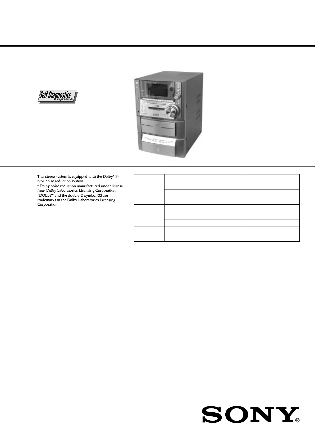
6
TABLE OF CONTENTS
MODEL IDENTIFICATION
— BACK PANEL —
•Abbreviation
G : German model
AED : North European model
MX : Mexican model
AR : Argentine model
HK : Hong Kong model
MY : Malaysia model
SP : Singapore model
KR : Korean model
AUS : Australian model
MODEL
US model
AEP, UK, G,AED, CIS model
MY, SP model
E model
AR model
HK model
MX model
AUS model
KR model
PARTS No.
4-227-556-0s
4-227-556-2s
4-227-556-3s
4-227-556-4s
4-227-556-5s
4-227-556-6s
4-227-556-7s
4-227-556-8s
4-227-556-9s
Parts No.
1. SERVICING NOTES ............................................. 7
2. GENERAL ........................................................................ 15
3. DISASSEMBLY
3-1. Case .................................................................................. 18
3-2. Front Panel Section .......................................................... 18
3-3. MD Mechanism Section
Tape Mechanism Deck Section (TCM-230AWR12)........ 19
3-4. Back Panel Section ........................................................... 19
3-5. MD Mechanism Deck Section (MDM-7B)...................... 20
3-6. Main Board, Front AMP Board ........................................ 20
3-7. CD Base Unit (BU-K4BD40)........................................... 21
3-8. CD Mechanism Deck Section (CDM53F-K4BD40)........ 21
3-9. Fitting Base (Guide) Assy, Bracket (Chassis) and
Fitting Base (Magnet) Assy ..............................................22
3-10. Tray (Sub) ......................................................................... 22
3-11. Chassis (Mold B) Section, Stocker Section and
Slider (Selection) ............................................................. 23
3-12. Gears Installation.............................................................. 23
3-13. Slider (Selection) Installation ........................................... 24
3-14. Stocker Section Installation .............................................. 24
3-15. Chassis (Mold B) Section Installation.............................. 25
3-16. BD Board.......................................................................... 25
4.TEST MODE...................................................................... 26
5. MECHANICAL ADJUSTMENTS............................... 35
6. ELECTRICAL ADJUSTMENTS................................. 35
7. DIAGRAMS
7-1. Circuit Boards Location ...................................................... 51
7-2. Block Diagrams
•CD Section ....................................................................... 54
•MD Section ...................................................................... 55
•SYSCON/SERVO Section ............................................... 56
•MAIN Section.................................................................. 57
7-3. Printed Wiring Board –Deck Section –.............................. 58
7-4. Schematic Diagram –Deck Section –................................ 59
7-5. Printed Wiring Board –CD Section –................................. 60
7-6. Schematic Diagram –CD Section –................................... 61
7-7. Printed Wiring Board –MD Section –................................ 62
7-8. Schematic Diagram –MD (1/2) Section –.......................... 63
7-9. Schematic Diagram –MD (2/2) Section –.......................... 64
7-10. Printed Wiring Board –Main Section –........................... 65
7-11. Schematic Diagram –Main (1/4) Section –..................... 66
7-12. Schematic Diagram –Main (2/4) Section –..................... 67
7-13. Schematic Diagram –Main (3/4) Section –..................... 68
7-14. Schematic Diagram –Main (4/4) Section –..................... 69
7-15. Printed Wiring Board –Digital (Side A) Section –.......... 70
7-16. Printed Wiring Board –Digital (Side B) Section –.......... 71
7-17. Schematic Diagram –Digital (1/2) Section –.................. 72
7-18. Schematic Diagram –Digital (2/2) Section –.................. 73
7-19. Printed Wiring Board
–AMP (US, AEP, UK, G, AED, CIS model) Section –.. 74
7-20. Schematic Diagram
–AMP (US, AEP, UK, G, AED, CIS model) Section –.. 75
7-21. Printed Wiring Board –AMP (E, MX,AR, HK,
MY, SP, KR, AUS model) Section –................................ 76
7-22. Schematic Diagram –AMP (E, MX,AR, HK,
MY, SP, KR, AUS model) Section –................................ 77
7-23. Printed Wiring Board –Panel Section –........................... 78
7-24. Schematic Diagram –Panel Section –............................. 79
7-25. Printed Wiring Board –Switch Section –........................ 80
7-26. Schematic Diagram –Switch Section –........................... 81
7-27. Printed Wiring Board –CD Mechanism Section –.......... 82
7-28. Schematic Diagram –CD Mechanism Section –............. 83
7-29. Printed Wiring Board –Leaf SW Section –..................... 84
7-30. Schematic Diagram –Leaf SW Section –........................ 84
7-31. Printed Wiring Board –MIC Section –............................ 85
7-32. Schematic Diagram –MIC Section –............................... 85
7-33. Printed Wiring Board –Power Supply (US, AEP, UK,
G, AED, CIS model) Section –........................................ 86
7-34. Schematic Diagram –Power Supply (US, AEP, UK,
G, AED, CIS model) Section –........................................ 87
7-35. Printed Wiring Board –Power Supply (E, MX, AR, HK,
MY, SP, KR, AUS model) Section –................................ 88
7-36. Schematic Diagram –Power Supply (E, MX, AR, HK,
MY, SP, KR, AUS model) Section –................................ 89
7-37. IC Block Diagrams........................................................... 90
7-38. IC Pin Functions............................................................... 94
8. EXPLODEDVIEWS
8-1. Back Panel Section ......................................................... 106
8-2. Front Panel Section ........................................................ 107
8-3. Chassis Section ............................................................... 108
8-4. CD Mechanism Deck Section-1 ..................................... 109
8-5. CD Mechanism Deck Section-2 ..................................... 110
8-6. Base Unit Section ........................................................... 111
8-7. Tape Mechanism Deck Section-1 ................................... 112
8-8. Tape Mechanism Deck Section-2 ................................... 113
8-9. MD Mechanism Section-1.............................................. 114
8-10. MD Mechanism Section-2.............................................. 115
9. ELECTRICAL PARTS LIST ...................................... 117