Sony LBT-LX5 User manual

SERVICE MANUAL
MICROFILM
Sony Corporation
Home Audio Division Company
COMPACT Hi-Fi STEREO SYSTEM
2000A001685-1
Printed in Japan ©2000.1
Published by Quality Assurance Dept.
9-929-066-11
US Model
LBT-LX30/LX50
Canadian Model
LBT-LX50
AEP Model
UK Model
LBT-LX5
E Model
Australian Model
LBT-LX6
COMPONENT MODEL NAME FOR LBT-LX5/LX6/LX30/LX50
• LBT-LX5/LX6/LX30/LX50 is composed following models.
Asfortheservicemanual,itisissuedforeachcomponentmodel,
then, please refer to it.
COMPACT DISC DECK
RECEIVER SYSTEM
SPEAKER SYSTEM SS-LX5
PARTS LIST
Ref No. Description Remark
ACCESSORIES & PACKING MATERIALS
********************************
1-475-572-41 COMMANDER, STANDARD (RM-SR5B)
1-501-374-11 ANTENNA, LOOP (AM)
1-501-804-11 ANTENNA (FM)
1-775-512-21 CORD, SPEAKER CONNECTION (FOR SPEAKER)
4-210-254-01 CUSHION (FOOT)(FOR SPEAKER)
4-227-074-12 MANUAL, INSTRUCTION (ENGLISH)
4-227-074-21 MANUAL, INSTRUCTION (FRENCH)(CND, EA)
4-227-074-31 MANUAL, INSTRUCTION (SPANISH)(MX, AR)
4-227-074-41 MANUAL, INSTRUCTION (FRENCH, SPANISH)(AEP, E, MY, SP)
4-227-074-51 MANUAL, INSTRUCTION (GERMAN, DUTCH, SWEDISH)(AEP)
4-227-074-61 MANUAL, INSTRUCTION (ITALIAN, PORTUGUESE)(AEP)
4-227-074-71 MANUAL, INSTRUCTION (POLISH, RUSSIAN)(CIS)
4-227-074-81 MANUAL, INSTRUCTION (ARABIC)(EA)
4-227-074-91 MANUAL, INSTRUCTION (CHINESE)(MY, SP)
4-227-075-11 MANUAL, INSTRUCTION (CZECH)(CIS)
4-227-075-21 MANUAL, INSTRUCTION (HUNGARIAN)(CIS)
4-227-075-31 MANUAL, INSTRUCTION (GREEK)(CIS)
4-227-075-41 MANUAL, INSTRUCTION (TURKISH)(CIS)
4-228-574-11 MANUAL, INSTRUCTION (ENGLISH, FRENCH, GERMAN, SPANISH, DUTCH,
SWEDISH, ITALIAN, PORTUGUESE, POLISH, RUSSIAN, DANISH, FINNISH,
HUNGARIAN, CZECH, GREEK, TURKISH) (SS-LX5)
4-991-151-31 COVER, BATTERY (FOR RM-SR5B)
LBT-LX5/LX6/LX30/LX50
HCD-LX5 HCD-LX6 HCD-LX30 HCD-LX50
LBT-LX5 LBT-LX6 LBT-LX30 LBT-LX50
SS-LX6
• Abbreviation
AR : Argentine
EA : Saudi Arabia
MY : Malaysia
SP : Singapore

SERVICE MANUAL
COMPACT Hi-Fi STEREO SYSTEM
US Model
HCD-LX30/LX50
Canadian Model
HCD-LX50
AEP Model
UK Model
HCD-LX5
E Model
Australian Model
HCD-LX6
SPECIFICATIONS
HCD-LX5/LX6/LX30/LX50
Photo: HCD-LX50
Dolby noise reduction manufactured under license
from Dolby Laboratories Licensing Corporation.
“DOLBY” and the double-D symbol ;are trade-
marks of Dolby Laboratories Licensing Corporation.
Model Name Using Similar Mechanism HCD-D290/G3300/XB3
CD Mechanism Type CDM37M-5BD32L
Base Unit Name BU-5BD32L
Optical Pick-up Name KSS-213D/Q-NP
Model Name Using Similar Mechanism HCD-DR4
Tape Transport Mechanism Type TCM-230PWR1
HCD-LX5/LX6/LX30/LX50 are the
Amplifier, CD player, Tape Deck and Tuner
section in LBT-LX5/LX6/LX30/LX50.
CD
Section
TAPE
Section
– Continued on next page –

2
ATTENTION AU COMPOSANT AYANT RAPPORT
À LA SÉCURITÉ!
LES COMPOSANTS IDENTIFIÉS PAR UNE MARQUE 0
SUR LES DIAGRAMMES SCHÉMATIQUES ET LA LISTE
DES PIÈCES SONT CRITIQUES POUR LA SÉCURITÉ
DE FONCTIONNEMENT. NE REMPLACER CES COM-
POSANTS QUE PAR DES PIÈCES SONY DONT LES
NUMÉROS SONT DONNÉS DANS CE MANUEL OU
DANS LES SUPPLÉMENTS PUBLIÉS PAR SONY.
SAFETY-RELATED COMPONENT WARNING!!
COMPONENTS IDENTIFIED BY MARK 0OR DOTTED
LINE WITH MARK 0ON THE SCHEMATIC DIAGRAMS
AND IN THE PARTS LIST ARE CRITICAL TO SAFE
OPERATION. REPLACE THESE COMPONENTS WITH
SONY PARTS WHOSE PART NUMBERS APPEAR AS
SHOWN IN THIS MANUAL OR IN SUPPLEMENTS PUB-
LISHED BY SONY.

3
SECTION 1
SERVICING NOTES
1. SERVICING NOTES ............................................... 3
2. GENERAL
Location of Controls ....................................................... 4
Setting the Time .............................................................. 6
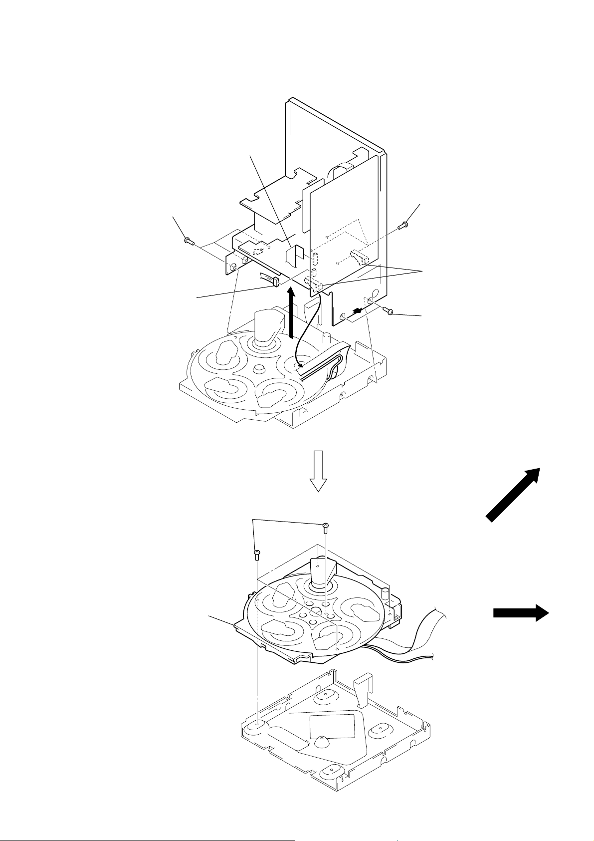
3. DISASSEMBLY ......................................................... 7
4. DIAGRAMS
4-1. Note for Printed Wiring Boards and
Schematic Diagrams ....................................................... 11
4-2. Printed Wiring Board – BD Board – .............................. 12
4-3. Schematic Diagram – BD Board – ................................ 13
4-4. Printed Wiring Boards – CD MOTOR Section – .......... 14
4-5. Schematic Diagram – CD MOTOR Section – .............. 15
4-6. Printed Wiring Board – AUDIO Board – ...................... 16
4-7. Schematic Diagram – AUDIO Board – ......................... 17
4-8. Printed Wiring Board – LEAF SW Board –.................. 18
4-9. Schematic Diagram – LEAF SW Board –..................... 18
4-10. Printed Wiring Board – MAIN Board – ........................ 19
4-11. Schematic Diagram – MAIN Board (1/3) – .................. 20
4-12. Schematic Diagram – MAIN Board (2/3) – .................. 21
4-13. Schematic Diagram – MAIN Board (3/3) – .................. 22
4-14. Printed Wiring Board – PANEL FL Board –................. 24
4-15. Schematic Diagram – PANEL FL Board –.................... 25
4-16. Printed Wiring Board – PANEL VR Board – ................ 26
4-17. Schematic Diagram – PANEL VR Board –................... 27
4-18. Printed Wiring Boards – TC-A/TC-B/CD-L/
CD-L2/CD-R/CD-R2 Boards – ...................................... 28
4-19. Schematic Diagram – TC-A/TC-B/CD-L/
CD-L2/CD-R/CD-R2 Boards – ...................................... 29
4-20. Printed Wiring Boards – FRONT INPUT/
HEADPHONE/MIC Boards – ........................................ 30
4-21. Schematic Diagram – FRONT INPUT/
HEADPHONE/MIC Boards – ........................................ 31
4-22. Printed Wiring Board – PA Board – .............................. 32
4-23. Schematic Diagram – PA Board – ................................. 33
4-24. Printed Wiring Boards – TRANS/SUB TRANS
(LX5/LX30/LX50) Boards – .......................................... 34
4-25. Schematic Diagram – TRANS/SUB TRANS
(LX5/LX30/LX50) Boards – .......................................... 35
5. EXPLODED VIEWS................................................ 38
6. ELECTRICAL PARTS LIST ............................... 46
TABLE OF CONTENTS
SAFETY CHECK-OUT
After correcting the original service problem, perform the follow-
ing safety check before releasing the set to the customer:
Check the antenna terminals, metal trim, “metallized” knobs,
screws, and all other exposed metal parts for AC leakage.
Check leakage as described below.
LEAKAGE TEST
TheAC leakage from any exposed metal part to earth ground and
from all exposed metal parts to any exposed metal part having a
return to chassis, must not exceed 0.5 mA (500 microamperes.).
Leakage current can be measured by any one of three methods.
1. A commercial leakage tester, such as the Simpson 229 or RCA
WT-540A. Follow the manufacturers’instructions to use these
instruments.
2. A battery-operatedAC milliammeter. The Data Precision 245
digital multimeter is suitable for this job.
3. Measuring the voltage drop across a resistor by means of a
VOM or battery-operated AC voltmeter. The “limit” indica-
tion is 0.75 V, so analog meters must have an accurate low-
voltage scale. The Simpson 250 and Sanwa SH-63Trd are ex-
amples of a passive VOM that is suitable. Nearly all battery
operated digital multimeters that have a 2VAC range are suit-
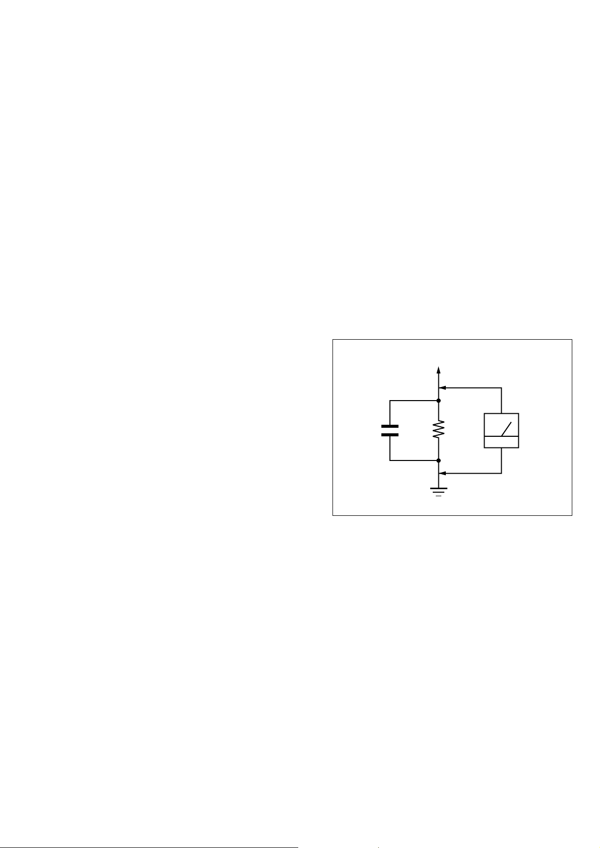
able. (See Fig. A)
Fig. A. Using an AC voltmeter to check AC leakage.
1.5 k
Ω
0.15 µF
AC
voltmeter
(0.75 V)
To Exposed Metal
Parts on Set
Earth Ground

4
This appliance is classified as a CLASS 1 LASER product.
The CLASS 1 LASER PRODUCT MARKING is located on
the rear exterior.
Laser component in this product is capable of emitting radiation
exceeding the limit for Class 1.
The following caution label is located inside the unit.
The laser diode in the optical pick-up block may suffer electro-
static break-down because of the potential difference generated
by the charged electrostatic load, etc. on clothing and the human
body.
During repair, pay attention to electrostatic break-down and also
use the procedure in the printed matter which is included in the
repair parts.
The flexible board is easily damaged and should be handled with
care.
NOTES ON LASER DIODE EMISSION CHECK
The laser beam on this model is concentrated so as to be focused
on the disc reflective surface by the objective lens in the optical
pick-up block. Therefore, when checking the laser diode emis-
sion, observe from more than 30 cm away from the objective lens.
Notes on chip component replacement
• Never reuse a disconnected chip component.
• Notice that the minus side of a tantalum capacitor may be dam-
aged by heat.
Flexible Circuit Board Repairing
• Keep the temperature of the soldering iron around 270 ˚C dur-
ing repairing.
• Do not touch the soldering iron on the same conductor of the
circuit board (within 3 times).
• Be careful not to apply force on the conductor when soldering
or unsoldering.
NOTES ON HANDLING THE OPTICAL PICK-UP
BLOCK OR BASE UNIT
CAUTION
Use of controls or adjustments or performance of procedures
other than those specified herein may result in hazardous ra-
diation exposure.
SECTION 2
GENERAL
LOCATION OF CONTROLS
– Front Panel –
1
wf
ws
wd
ql
wa
w;
qk
qj
5
7
6
8
9
0
qa
qs
qd
qfqgqh
2 43
2
1
9
8
7
6
5
4 3
– Rear Panel –

5
1?/1(POWER) button
2DAILY button
REC button
SLEEP button
c/CLOCK SET button
3Display
4SYNC EQ button
SYNC BASS button
SURROUND button
MIX GUITAR/KARAOKE button
5FUNCTION button
6v/B/V/bbutton
7VOLUME control
8DECK B
9PHONES jack
0DECK B operating button
gbutton Gbutton xbutton
mbutton Mbutton Xbutton
zREC button HI SPEED DUB button
CD SYNC button
qa .AMS >control
qs CD operating button
GXbutton xbutton mbutton
Mbutton DISC SKIP button
qd VIDEO 2 INPUT jack
qf PLAY MODE button
REPEAT button
qg ZA EJECT
ZB EJECT
qh DISC1-5 button
qj LOOP button
FLASH button
NON-STOP button
EDIT button
qk DECK A operating button
gbutton Gbutton xbutton
mbutton Mbutton
DIRECTION button
DOLBY NR button
ql MIC MIX jack
GUITAR jack
w; DECK A
wa SUPPER WOOFER MODE button
MIC LEVEL control
GUITAR LEVEL control
ws EJECT button
GROOVE button
SUPER WOOFER button
wd TUNER/BAND button
TUNING +/– button
ENTER/NEXT button
TUNER MEMORY button
STEREO/MONO button
TUNING MODE button
PTY button (LX5 only)
wf POWER SAVE/DEMO (STAND BY) button
DISPLAY button
SPECTRUM ANALYZER button
1DJ MIX jack
2ANTENNA terminal
3REAR SURROUND SPEAKER terminal (LX50 only)
4FRONT SPEAKER terminal
5CD DIGITAL OUT terminal
6VIDEO OUT jack
7VIDEO 1 jack
8MD IN/OUT jack
9PHONO IN jack

6

7
CASE
FRONT PANEL SECTION
Note: Follow the disassembly procedure in the numerical order given.
SECTION 3
DISASSEMBLY
2five screws
(BVTT3 ×6)
6case
3two screws
(BVTP3 ×8)
1three screws
(CASE3 TP2)
1three screws
(CASE3 TP2)
4
4
5
5
5four screws
(BVTP3 ×8)
5screw (BVTP3 ×8)
2connector
(CN802)
4two lugs
6claw
3screw
(BVTP3 ×8
)
2two connectors
(CN452, 702)
1wire (flat type)
(15 core) (CN303)
1wire (flat type)
(17 core) (CN304)
1wire (flat type)
(13 core) (CN431)
3three screws
(BVTP3 ×8)
4lug
7front panel section
MAIN BOARD (Page 8)
CD MECHANISM DECK
(Page 9)

8
TAPE MECHANISM DECK (TCM-230PWR1)
MAIN BOARD
1wire (flat type) (17 core)
(CN1001)
2two screws
(BVTP3 ×8)
1wire (flat type) (15 core)
(CN601)
2two screws
(BVTP3 ×8)
3tape mechanism deck
(TCM-230PWR1)
7wire (flat type) (19 core)
(CN411)
2nine screws
(BVTP3 ×8)
6back panel
1wire (flat type) (15 core) (LX5)
wire (flat type) (13 core) (LX6/LX30/LX50)
(CN441)
3jumper plug
(LX5/LX6: Mexican/LX30/LX50)
2screw (BVTP3 ×8)
(LX5/LX6: Mexican/
LX30/LX50)
2three screws (BVTP3 ×8)
2screw (BVTP3 ×8)
(LX50)
2two screws (BVTP3 ×8)
5connector (CN903)
qa MAIN board
4
0two connector
(CN803, 804)
8connector
(CN412)
9two screws
(BVTP3 ×8)

9
CD MECHANISM DECK (CDM37M-5BD32L)
7five screws
(BVTP3 ×8)
8CD mechanism deck
(CDM37M-5BD32L)
3three screws
(BVTP3 ×8)
3three screws
(BVTP3 ×8)
2connector
(CN412)
1wire (flat type) (19 core)
(CN411)
5Open the two cable clamps.
4
4
6
3two screws
(BVTP3 ×8)

10
BASE UNIT (BU-5BD32L)
3base unit
(BU-5BD32L)
1BU fitting scre
w
2boss
DISC TABLE
Note: When the disc table is installed, adjust the positions of roller cam
and mark
B
as shown in the figure, then set to the groove of disc
table.
1two screws
(BVTP3 ×8)
A
2two brackets (BU)
3step screw
4disc tabl
e
A

1111
SECTION 4
DIAGRAMS
4-1. NOTE FOR PRINTED WIRING BOARDS AND SCHEMATIC DIAGRAMS
(In addition to this, the necessary note is printed in each block)
Note on Printed Wiring Board:
•X: parts extracted from the component side.
•Y: parts extracted from the conductor side.
•f: internal component.
•b: Pattern from the side which enables seeing.
(The other layers' patterns are not indicated.)
Caution:
Pattern face side: Partsonthe pattern facesideseen from
(Side B) the pattern face are indicated.
Parts face side: Parts on the parts face side seen from
(Side A) the parts face are indicated.
Note on Schematic Diagram:
• All capacitors are in µF unless otherwise noted. pF: µµF
50 WV or less are not indicated except for electrolytics
and tantalums.
• All resistors are in Ωand 1/4W or less unless otherwise
specified.
•f: internal component.
•2: nonflammable resistor.
•5: fusible resistor.
•C: panel designation.
•U: B+ Line.
•V: B– Line.
•H: adjustment for repair.
• Voltages aretaken with aVOM(Input impedance10 MΩ).
Voltage variations may be noted due to normal produc-
tion tolerances.
• Waveforms are taken with a oscilloscope.
Voltage variations may be noted due to normal produc-
tion tolerances.
• Circled numbers refer to waveforms.
• Signal path.
F: TUNER (FM/AM)
E: PLAYBACK (DECK A)
d: PLAYBACK (DECK B)
G: RECORD
J: CD PLAY (ANALOG OUT)
c: CD PLAY (DIGITAL OUT)
N: MIC INPUT
• Abbreviation
AUS : Australian model
AR : Argentine model
EA : Saudi Arabia model
MY : Malaysia model
MX : Mexican model
SP : Singapore model
Note:
The components identi-
fied by mark 0or dotted
linewith mark 0are criti-
cal for safety.
Replace only with part
number specified.
Note:
Lescomposants identifiéspar
une marque 0sont critiques
pour la sécurité.
Ne les remplacer que par une
pièce portant le numéro
spécifié.
• Circuit Boards Location
PANEL FL board
TRANS board
SUB TRANS board
(LX5/LX30/LX50)
TUNER (FM/AM)
MAIN board
PA board
HEADPHONE boar
d
TC-B board
CD-R board FRONT INPUT board
CD-L board
TC-A board
MIC board
PANEL VR board
LEAF SW board TABLE SENSOR board
BD boar
d
AUDIO board
LED board
CD MOTOR board
•Indication of transisitor.
C
BThese are omitted.
E
Q
B
These are omitted.
CE
Q
B
These are omitted.
CE
Q

1212
HCD-LX5/LX6/LX30/LX50
4-2. PRINTED WIRING BOARD – BD Board – • See page 11 for Circuit Boards Location.
05 05
KSS-213D/Q-NP
19
)(
)(
)(
TP(VC)
TP(RF)
TP(TE)
TP(FE1)
TP(FE)
TP
(AGCCON)
TP(GND)
21
21
31
31
,
,
21
21
31
31
,
,
• Semiconductor
Location
(Side A)
Ref. No. Location
Q101 C-3
• Semiconductor
Location
(Side B)
Ref. No. Location
IC101 C-2
IC102 B-1
IC103 B-1
(Page 19)

1313
HCD-LX5/LX6/LX30/LX50
4-3. SCHEMATIC DIAGRAM – BD Board – • See page 23 forWaveforms. •See page 36 for IC Block Diagrams.
• Voltages and waveforms are dc with respect to ground
under no-signal conditions.
no mark : CD STOP
( ) : CD PLAY
The components identified by mark 0or dotted
line with mark 0are critical for safety.
Replaceonly withpart numberspecified.
Lescomposantsidentifiés parunemarque 0sont
critiques pour la sécurité. Ne les remplacer que
par une pièce portant le numéro spécifié.
(Page 21)

1414
HCD-LX5/LX6/LX30/LX50
B
C
D
D
C
4-4. PRINTED WIRING BOARDS – CD MOTOR Section – • See page 11 for Circuit Boards Location.
(Page 19)TO
LED BOARD
TO
TABLE SENSOR BOARD
TO
CD MOTOR BOARD
TO
CD MOTOR BOARD

1515
HCD-LX5/LX6/LX30/LX50
4-5. SCHEMATIC DIAGRAM – CD MOTOR Section – •See page 36 for IC Block Diagrams.
B
• Voltages are dc with respect to ground under no-signal
conditions.
no mark : CD STOP
(Page 21)

1616
HCD-LX5/LX6/LX30/LX50
4-6. PRINTED WIRING BOARD – AUDIO Board – • See page 11 for Circuit Boards Location.
05
E
()
(Page 19)

1717
HCD-LX5/LX6/LX30/LX50
4-7. SCHEMATIC DIAGRAM – AUDIO Board – • See page 36 for IC Block Diagrams.
• Voltages are dc with respect to ground under no-signal
conditions.
no mark : TAPE PLAY
( ) : RECORD
The components identified by mark 0or dotted
line with mark 0are critical for safety.
Replaceonly withpart numberspecified.
Lescomposantsidentifiés parunemarque 0sont
critiques pour la sécurité. Ne les remplacer que
par une pièce portant le numéro spécifié.
PB LEVEL (L)
(DECK A)
PB LEVEL (R)
(DECK A)
PB LEVEL (L)
(DECK B)
PB LEVEL (R)
(DECK B)
PB EQ AMP
(DECK A)
PB EQ AMP
(DECK B)
SWITCHING
REC BIAS (L)
(DECK B)
REC BIAS (R)
(DECK B)
BIAS OSC
REC BIAS
-6.8
(PLAYBACK)
E
NC
A +7.5V
APB–LCH
APB–RCH
AGND
BPB–LCH
BPB–RCH
A –7.5V
–VBIAS (–7.5V)
+VBIAS (+7.5V)
B–REC–RCH
B–REC–LCH
TC–HEAD–GND
(Page21)

1818
HCD-LX5/LX6/LX30/LX50
4-8. PRINTED WIRING BOARD – LEAF SW Board – • See page 11 for Circuit Boards Location.
05
DECK A
PLUNGER
DECK B
PLUNGER
(DECK A PLAY)
(DECK A HALF) (DECK A 120/70) (DECK A REC)
(DECK B HALF)
(DECK B PLAY)
(DECK B 120/70)
(DECK B REC)
12
12
F
4
12
34
12
3
()
4-9. SCHEMATIC DIAGRAM – LEAF SW Board –
DECK B
PLUNGER DECK A
PLUNGER
(CAPSTAN)
(DECK A 120/70)
(DECK A HALF)
(DECK A REC)
(DECK B HALF)
(DECK B REC)
(DECK B 120/70)
ROTATION DETECT SENSOR
(DECK A)
ROTATION DETECT
SENSOR (DECK B)
(DECK A PLAY) (DECK B PLAY)
F
CONTROL SWITCH
CAPM–
CAPM+
CAPM–H/L
A–TRGM
TRGM–GND
B–TRGM
A–SHUT
DGND
A–HALF
+5V
A–120/70
B–SHUT
A PLAY
B–HALF / REC–A / REC–B
B–120/70
B PALY
NC
• Voltages are dc with respect to ground under no-signal
conditions.
no mark : TAPE PLAY
( ) : RECORD
∗: Impossible to measure
(Page 19)
(Page 21)

1919
HCD-LX5/LX6/LX30/LX50
4-10. PRINTED WIRING BOARD – MAIN Board – • See page 11 for Circuit Boards Location.
• Semiconductor
Location
Ref. No. Location
D191 B-7
D192 B-7
D193 A-6
D194 B-6
D333 I-3
D334 I-3
D335 I-4
D336 I-4
D501 I-6
D534 G-7
D801 I-6
D802 H-7
D803 H-8
D804 I-7
D805 H-8
D806 H-7
D807 H-8
D808 I-6
D911 E-10
D912 F-9
D913 F-10
D931 G-10
D951 B-10
IC101 D-3
IC181 B-5
IC191 B-7
IC301 G-2
IC501 H-6
IC601 B-1
IC781 A-12
IC801 I-7
IC901 C-11
IC911 E-10
IC931 G-10
IC932 G-11
IC932 G-12
IC933 H-11
IC951 B-11
Q111 D-5
Q112 D-5
Q113 D-5
Q115 D-4
Q161 E-5
Q162 E-5
Q163 E-5
Q165 E-3
Q331 I-2
Q332 I-2
Q333 I-2
Q334 I-2
Q335 I-4
Q336 I-3
Q337 I-3
Q338 I-4
Q339 I-4
Q340 I-3
Q341 I-3
Q342 I-3
Q343 I-3
Q801 H-7
Q802 H-9
Q803 H-8
Q804 I-8
Q901 C-11
Q902 B-11
Q903 B-11
Q904 B-11
Q905 B-11
Q906 B-11
Q911 F-9
Q912 F-9
Q913 F-9
Q914 F-9
Q931 G-10
Q932 G-9
Q961 A-10
Q962 A-10
(Page 26)
(Page 16)
(Page 18)
(Page 30)
(Page 32)
(Page 32)
(Page 14)(Page 12)
(Page 24)
This manual suits for next models
3
Table of contents
Other Sony Stereo System manuals

Sony
Sony MHC-DX8 User manual

Sony
Sony MHC-V83D User manual

Sony
Sony SS-CCQ1 User manual

Sony
Sony FH-SR1D User manual

Sony
Sony PHC-ZW770L User manual

Sony
Sony ZS-XN30 - Cd Boombox User manual

Sony
Sony LBT-GPX55 User manual

Sony
Sony ZS-S10CP Instruction Manual

Sony
Sony CAS-1 User manual

Sony
Sony MEX-BT3750U User manual

Sony
Sony HCD-GRX9900 User manual

Sony
Sony PMC-DR50L User manual

Sony
Sony CMT-DH7BT - Micro Hi Fi Component System User manual

Sony
Sony HCD-RG55 User manual

Sony
Sony LBT-ZX9 User manual

Sony
Sony MHC-RG295 User manual

Sony
Sony MHC-VX90AV User manual

Sony
Sony MHC-GRX990 User manual

Sony
Sony XDR-DS16iPN User manual

Sony
Sony SEN-311 User manual