Sony PMC-107L User manual

– 1 –
CD Model Name Using Similar Mechanism CFD-222L
Section CD Mechanism Type KSM-213CDM
Optical Pick-up Name KSS-213C
TC Model Name Using Similar Mechanism NEW
Section Tape Transport Mechanism Type MF-107
SERVICE MANUAL
AEP Model
UK Model
Singapore Model
PMC-107L
PERSONAL COMPONENT SYSTEM
MICROFILM
CD player section
System
Compact disc digital audio system
Laser diode properties
Material: GaAlAs
Wave length: 780 nm
Emission duration: Continuous
Laser output: Less than 44.6 µW
(This output is the value measured at a distance of
about 200 mm from the objective lens surface on
the optical pick-up block with 7 mm aperture.)
Spindle speed
200 r/min (rpm) to 500 r/min (rpm) (CLV)
Number of channels
2
Frequency response
20 - 20,000 Hz +1/–2 dB
Wow and flutter
Below measurable limit
Radio section
Frequency range
FM AEP, UK, Singapore model 87.6 - 107 MHz
Italian model 87.5 - 108 MHz
East European model 65 - 74 MHz
87.5 - 108 MHz
MW 531 - 1,602 kHz
LW 153 - 279 kHz
IF FM: 10.7 MHz
MW/LW: 450 kHz
Aerials
FM: Wire aerial
MW/LW: External aerial
SPECIFICATIONS
– Continued on next page –
Cassette-corder section
Recording system
4-track 2 channel stereo
Fast winding time
Approx. 120 s (sec.) with Sony cassette C-60
Frequency response
TYPE I (normal): 70 - 10,000 Hz
General
Speaker
Full range: 10 cm (4 in.) dia.,
3 ohms, cone type (2)
Outputs
Headphones jack (stereo minijack)
For 16 - 68 ohms impedance headphones
Maximum power output
5 W + 5 W
Power requirements
For personal component system:
230 V AC, 50 Hz
For remote control:
3 V DC, 2 R6 (size AA) batteries
Power consumption
AC 23 W
Ver 1.1 1998. 08

– 2 –
SAFETY-RELATED COMPONENT WARNING!!
COMPONENTS IDENTIFIED BY MARK !OR DOTTED LINE
WITH MARK !ON THE SCHEMATIC DIAGRAMS AND IN
THE PARTS LIST ARE CRITICAL TO SAFE OPERATION.
REPLACE THESE COMPONENTS WITH SONY PARTS WHOSE
PART NUMBERS APPEAR AS SHOWN IN THIS MANUAL OR
IN SUPPLEMENTS PUBLISHED BY SONY.
Dimensions (incl. projecting parts)
Player :Approx. 160 ×245 ×215 mm (w/h/d)
(6 3/8 ×9 3/4 ×8 1/2 inches)
Speaker :Approx. 150 ×245 ×175 mm (w/h/d)
(6 ×9 3/4 ×7 inches)
MassPlayer :Approx. 2.6 kg (5 lb. 12 oz.)
Speaker :Approx. 1.1 kg (2 lb. 7 oz.)
Supplied accessories
Remote control (RMT-C107AD) (1)
(Except East European model)
Remote control (RMT-C107A) (1)
(East European model)
MW/LW loop aerial (1)
Conversion plug adaptor (1) (UK)
Design and specifications are subject to change without
notice.
This Compact Disc player is
classified as a CLASS 1
LASER product.
The CLASS 1 LASER
PRODUCT label is located
on the bottom exterior.
CAUTION
Use of controls or adjustments or performance of proce-
dures other than those specified herein may result in haz-
ardous radiation exposure.
Flexible Circuit Board Repairing
•Keep the temperature of the soldering iron around 270˚C during
repairing.
•Do not touch the soldering iron on the same conductor of the
circuit board (within 3 times).
•Be careful not to apply force on the conductor when soldering
or unsoldering.
Notes on Chip Component Replacement
•Never reuse a disconnected chip component.
•Notice that the minus side of a tantalum capacitor may be dam-
aged by heat.
NOTES ON HANDLING THE OPTICAL PICK-UP BLOCK
OR BASE UNIT
The laser diode in the optical pick-up block may suffer electrostatic
breakdown because of the potential difference generated by the
charged electrostatic load, etc. on clothing and the human body.
During repair, pay attention to electrostatic breakdown and also use
the procedure in the printed matter which is included in the repair
parts.
The flexible board is easily damaged and should be handled with
care.
NOTES ON LASER DIODE EMISSION CHECK
The laser beam on this model is concentrated so as to be focused on
the disc reflective surface by the objective lens in the optical pick-
up block. Therefore, when checking the laser diode emission,
observe from more than 30 cm away from the objective lens.
CHUCK PLATE JIG ON REPAIRING
On repairing CD section, playing a disc without the CD lid, use
Chuck Plate jig.
• Part No. of Chuck Plate jig : X-4918-255-1
LASER DIODE AND FOCUS SEARCH OPERATION
CHECK
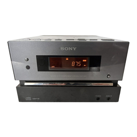
1. Open the CD lid.
2. Push on PUSH SWITCH (SW701) as following figure.
3. Confirm the laser diode emission while observing the objecting
lens. When there is no emission, Auto Power Control circuit or
Optical Pick-up is broken.
Objective lens moves up and down once for the focus search.
Push on SW701 in the
arrowed direction with
a screwdriver, etc.
SW701
– 3 –
TABLE OF CONTENTS
1. GENERAL
Playing a CD ........................................................................... 4
Listening to the radio............................................................... 5
Playing a tape .......................................................................... 6
Recording on a tape ................................................................. 7
2. DISASSEMBLY
2-1. Front Cabinet Assy .............................................................. 8
2-2. CD Chassis Assy ................................................................. 9
2-3. Power Board ........................................................................ 9
2-4. Main Board ....................................................................... 10
2-5. CD Board .......................................................................... 10
2-6. Optical Pick-up ................................................................. 11
2-7. Mechanism Deck Block .................................................... 11
2-8. Control Board.................................................................... 12
3. MECHANICAL ADJUSTMENTS ............................... 13
4. ELECTRICAL ADJUSTMENTS
Tape Section .......................................................................... 13
Tuner Section......................................................................... 14
CD Section ............................................................................ 16
5. DIAGRAMS
5-1. IC Pin Description............................................................. 20
5-2. Circuit Boards Location .................................................... 22
5-3. Block Diagram –CD Section–...........................................23
5-4. Block Diagram –Main Section–........................................ 25
5-5. Printed Wiring Boards –CD Section– ............................... 27
5-6. Schematic Diagram –CD Section–.................................... 29
5-7. Printed Wiring Boards –Panel Section– ............................ 31
5-8. Schematic Diagram –Panel Section– ................................ 33
5-9. Printed Wiring Boards –Main Section– ............................35
5-10. Schematic Diagram –Main Section (1/2)– ........................ 37
5-11. Schematic Diagram –Main Section (2/2)– ........................ 39
6. EXPLODEDVIEWS
6-1. Rear Cabinet Section......................................................... 44
6-2. Front Cabinet Section........................................................45
6-3. Upper Cabinet Section ...................................................... 46
6-4. Cassette Mechanism Section-1 ......................................... 47
6-5. Cassette Mechanism Section-2 ......................................... 48
6-6. Cassette Mechanism Section-3 ......................................... 49
6-7. Cassette Mechanism Section-4 ......................................... 50
6-8. Optical Pick-up Section..................................................... 51
6-9. Speaker Section ................................................................. 52
7. ELECTRICAL PARTS LIST......................................... 53

– 4 –
SECTION 1
GENERAL This section is extracted
from instruction manual.

– 5 –

– 6 –

– 7 –

– 8 –
SECTION 2
DISASSEMBLY
3
BVTP 3x14
1
BVTP 3x14
2
BVTP 3x1
4
4
CNP303
5
CNP301
9
CNP702
6
CNP302
7
CNP306
8
CNP308
0
front cabinet assy
• The equipment can be removed using the following procedure.
Set Front cabinet assy CD chassis assy Main board
Power board CD board Optical pick-up
Mechanism deck block
Control board
Note : Follow the disassembly procedure in the numerical order given.
2-1. FRONT CABINET ASSY

– 9 –
2-2. CD CHASSIS ASSY
2-3. POWER BOARD
2
BVTP 3x10
3
wire
5
CD chassis assy
1
BVTP 3x1
0
4
CNP901
2
BVTP 4x16
3
POWER board
1
CNP902

– 10 –
2-4. MAIN BOARD
2-5. CD BOARD
2
BVTP 3x10
1
CNP304
3
MAIN board
1
CNP701
2
CNP703
3
connector
5
BVTP 3x10
6
CD board
4
BVTP 3x10

– 11 –
2-6. OPTICAL PICK-UP
2-7. MECHANISM DECK BLOCK
3
optical pick-up
2
screws (2.6x16)
1
screws (2.6x16)
3
BVTP 3x8
2
BVTP 3x8
4
mechanism deck block
1
Open the cassette lid.

– 12 –
2-8. CONTROL BOARD
1
BVTP 3x8
2
BVTP 3x8
4
CONTROL board
3
CNP803

– 13 –
TAPE SECTION 0 dB = 0.775 V
• Standard Output Level
Output terminal HP OUT
load impedance 32 Ω
output signal level 0.25 V (–10 dB)
• Test Tape
Type Signal Used for
WS-48A 3 kHz, 0 dB tape speed adjustment
Tape Speed Adjustment
Procedure:
Mode: playback
PRECAUTION
1. Clean the following parts with a denatured-alcohol-moistened
swab :
record/playback head pinch roller
erase head rubber belts
capstan idlers
2. Demagnetize the record/playback head with a head demagne-
tizer. (Do not bring the head magnetizer close to the erase head.)
3. Do not use a magnetized screwdriver for the adjustments.
4. After the adjustments, apply suitable locking compound to the
parts adjusted.
5. The adjustments should be performed with the rated power
supply voltage unless otherwise noted.
Torque Measurement
Mode Torque meter Meter reading
FWD CQ-102C 30 – 70 g • cm
(0.42 – 0.97 oz • inch)
FWD CQ-102C 1.5 – 5.5 g • cm
Back Tension (0.021 – 0.076 oz • inch)
FF CQ-201B more than 60 g • cm
(more than 0.83 oz • inch)
REW CQ-201B more than 60 g • cm
(more than 0.83 oz • inch)
Tape Tension Measurement
Mode Tension meter Meter Reading
FWD CQ-403A more than 100 g
(more than 3.53 oz)
SECTION 4
ELECTRICAL ADJUSTMENTS
SECTION 3
MECHANICAL ADJUSTMENTS
1. Make sure that the value indicated on the frequency counter
falls into the specification.
2. If out of specification, adjust so that the value on the frequency
counter is 3 kHz.
Adjustment Value:
Digital frequency counter
2,985 to 3,015 Hz
Adjust so that the frequency at the beginning and that at the end of
tape winding are between 2,955 to 3,045 Hz.
Adjustment Location:
phones jack
set
32
Ω
test tape
WS-48A
(3 kHz, 0 dB)
digital frequency
counter
TAPE SPEED
Adjustment

– 14 –
FM FREQUENCY COVERAGE
ADJUSTMENT
Frequency Display 87.5 MHz 108 MHz
(65 MHz)
Reading on Digital voltmeter 1.8 ±0.2 V 5.6 ±0.2V
(0.9 ±0.2 V) (7.3 ±0.2 V)
Adjustment Part L6 <confirmation>
FM TRACKING ADJUSTMENT
Adjust for a maximum reading on level meter.
L5 CT1
87.5 MHz (68 MHz) 108 MHz (102 MHz)
MW FREQUENCY COVERAGE
ADJUSTMENT
Frequency Display 531 kHz 1,611 kHz
Reading on Digital voltmeter 0.9 ±0.1 V 5.6 ±0.2V
Adjustment Part L2 CT2
MW TRACKING ADJUSTMENT
Adjust for a maximum reading on level meter.
L9 CT4
621 kHz 1,404 kHz
LW FREQUENCY COVERAGE
ADJUSTMENT
Frequency Display 153 kHz 279 kHz
Reading on Digital voltmeter 0.6 ±0.1 V 5.3 ±0.2V
Adjustment Part CT3 <confirmation>
LW TRACKING ADJUSTMENT
Adjust for a maximum reading on level meter.
L10 CT5
162 kHz 261 kHz
( ) : East European model
Adjustment Location: See page 15.
TUNER SECTION 0 dB = 1 µV
• FM Section
Setting:
BAND switch: FM
22.5 kHz frequency
deviation by 400 Hz signal
output level :as low as possible
• MW/LW Section
Setting:
BAND switch: MW or LW
30% amplitude
modulation by
400 Hz signal
• Connecting Level Meter (FM, MW and LW)
• Connecting Digital Voltmeter (FM, MW and LW)
• Repeat the procedures in each adjustment several times, and the
frequency coverage and tracking adjustments should be finally
done by the trimmer capacitors.
TP (FM ANT)
FM RF signal
generator
0.01
µ
F
set
Put the lead-wire
antenna close to
the supplied MW/LW
loop antenna.
AM RF signal
generator
phones jack
set
32
Ω
level meter
(range: 0.5–5 V ac
)
digital
voltmeter
100 k
Ω
TP (VT)

– 15 –
Adjustment Location: main board
–main board (component side)–
MW
FREQUENCY
COVERAGE
Adjustment CT3
LW
FREQUENCY
COVERAGE
Adjustment
FM
TRACKING
Adjustment
TP (VT)
CT1
L6
FM
FREQUENCY
COVERAGE
Adjustment
L5
LW
TRACKING
Adjustment
CT5
L10
CT2
L2
MW
TRACKING
Adjustment CT4
L9
TP
(FM ANT)
R31

– 16 –
A
0V A=B
B
CD SECTION
Notes on Adjustment
1. Perform Traverse adjustment in test mode.
After adjustment, be sure to release test mode.
2. Perform adjustments in the order given.
3. Use the disc (YEDS-18, Part No. 3-702-101-01) only when so
indicated.
4. Short the both sides of R714 on the CD board for stop operation
of anti-shock circuit. (See page 19.)
• Switch position
FUNCTION switch : CD
• In case ofTest Mode
1. Short the solder bridge the TP801 (TEST) on the key board.
2. Insert the AC power plug.
• Release theTest Mode
Releasethe shortedsolder bridgethe TP801(TEST), thetest mode
is release.
Before Adjustment
Put the set into test mode and perform the following checks. Repair
if there are any problems.
• Sled Motor Check
Press the ±, ≠buttons and confirm that the optical pick-up
moves smoothly from the innermost to outermost circumference
and back smoothly and with no catching or abnormal noises.
±: Optical pick-up moves to the outer circumference
≠: Optical pick-up moves to the inner circumference
• Focus Search Check
1. Push the flbutton. (Focus search operation is performed
continuously.)
2. Look atthe opticalpick-upobjective lensand confirmthe itmoves
up and down smoothly, with no catching or abnormal noises.
3. Push the πbutton.
Confirm that focus search operation stops. If it does not, push the
πbutton again longer.
Traverse Adjustment
This adjustment is to be done when the optical pick-up block is
replaced.
Procedure:
1. Connect the oscilloscope between TP (TE) and TP (VC).
2. Put the set into test mode.
3. Push the CD lid to open and insert disc (YEDS-18).
4. Close the CD lid.
5. Press the ±and ≠buttons to move the optical pick-up to
the center.
6. Push the flbutton.
7. Push the πbutton.
8. Push the flbutton.
9. Adjust RV702 so that the oscilloscope traverse waveform is
symmetrical, as shown in the figure below.
10. Release test mode after adjustment is completed.
–key board (conductor side) –
Adjustment Location : See page 19.
oscilloscope
(DC range)
CD board
TP (TE)
TP (VC)
TP801
(TEST)

– 17 –
Gain
Symptoms Focus Tracking
• The time until music starts becomes longer
for πmflon automatic selection. low low or high
(≠, ±buttons pressed.)
(Normally, takes about 2 seconds.)
• Music does not start and disc continues
to rotate for πmflor automatic – low
selection.
(≠, ±buttons pressed.)
• Sound is interrupted during PLAY. Or – low
time counter display stops progressing.
• More noise during 2-axis device high high
operation.
Focus Bias Adjustment
This adjustment is to be done when the optical pick-up block is
replaced.
Procedure :
1. Connect the oscilloscope between TP (RF) and TP (VC).
2. Insert disc (YEDS-18) and push the flbutton.
3. Adjust RV701 so that the oscilloscope waveform is maximum as
shown in the figure below (eye pattern).
• RF signal reference waveform (eye pattern)
REFERENCE
Focus/Tracking Gain Adjustment
A frequency response analyzer is necessary in order to perform this
adjustment exactly.
However, this gain has a margin, so even if it is slightly off, there is
no problem. Therefore, do not perform this adjustment.
Focus/tracking gain determines the pick-up follow-up (vertical and
horizontal)relative to mechanicalnoise andmechanical shockwhen
the 2-axis device operate.
However, as these reciprocate, the adjustment is at the point where
both are satisfied.
• When gain raised, the noise when the 2-axis device operates
increases.
• When gain is lowered, it is more susceptible to machanical shock
and skipping occurs more easily.
When gain adjustment is off, the symptoms below appear.
When observing the eye pattern, set the oscilloscope for AC range
and raise vertical sensitivity.
Adjustment Location : See page 19.
oscilloscope
(DC range)
CD board
TP (RF)
TP (VC)
0V
1.1 – 1.5 V
VOLT / DIV : 0.2 V
TIME / DIV : 500 nS

– 18 –
The following is a simple adjustment method.
–SimpleAdjustment–
Note :Since exact adjustment cannot be performed, remember the
positions of the controls before performing the adjustment.
If the positions after the simple adjustment are only a little
different, return the controls to the original position.
Procedure:
1. Keep the set horizontal.
If the set not horizontal, this adjustment cannot be performed due
to the gravity against the 2-axis device.
2. Insert disc (YEDS-18) and push the flbutton.
3. Connect the oscilloscope between TP (FE) and TP (VC).
4. Adjustment RV704 so that the waveform is as shown in the
figure below. (focus gain adjustment)
• Correct Example
5. Connect the osilloscope between TP (TE) and TP (VC).
6. Adjust RV703 so that the waveform is as shown in the figure
below. (tracking gain adjustment)
• Correct Example
• Incorrect Examples (DC level changes more than on adjusted
waveform)
VOLT/DIV : 100 mV
TIME/DIV : 2 mS
0 V
100 mV
0 V
250 mV
VOLT/DIV : 100 mV
TIME/DIV : 2 mS
VOLT/DIV : 100 mV
TIME/DIV : 2 mS
0 V
75 mV
100 mV
• Incorrect Examples (fundamental wave appears)
VOLT/DIV : 100 mV
TIME/DIV : 2 mS
0 V
VOLT/DIV : 100 mV
TIME/DIV : 2 mS
0 V
0 V
VOLT/DIV : 100 mV
TIME/DIV : 2 mS
Adjustment Location : See page 19.
low focus gain
high focus gain
low tracking gain
high tracking gain
(higher fundamental wave than for low gain)
oscilloscope
(DC range)
CD board
TP (FE)
TP (TE)
TP (VC)

– 19 –
RV702
TRAVERSE
Adjustment
TP (RF)
TP (VC)
TP (FE)
TP (TE)
IC701
CNP701
R714
RV703
TRACKING GAIN
Adjustment
RV701
FOCUS BIAS
Adjustment
RV704
FOCUS GAIN
Adjustment
Adjustment Location: CD board
–CD board (conductor side)–

– 20 –
5-1. IC PIN DESCRIPTION
• IC801 CXP50716-082Q (SYSTEM CONTROL/LCD DRIVE)
Pin No. Pin Name I/O Pin Description
1 – 19 SEG0 – 18 O LCD drive segment output
20 – 23 COM0 – 3 O LCD drive common output
24 – 26 VLC-3 – 1 O LCD drive voltage terminal
27 VL O LCD drive port ON/OFF output
28 RMC I Sircs receiver input
29 C-SCOR I CD SCOR input
30 TX O Oscillation output (32.768 kHz)
31 TXE I Oscillation input (32.768 kHz)
32 RST I System reset input
33 N.C. — Not used.
34 VDD — Power supply pin (+5 V)
35 – 38 KEY1 – 4 I Key input
39 INIT O Tuner select initial setting output
40 VER I Tuner destination band select input
41 9K/10K I Tuner band 9k/10k select input
42 REG-CHK I Voltage detection input
43 N.C. — Not used.
44 C-SQCK O CD Sub-Q read clock output
45 C-SENS I CD SENSE input
46 C-SQSO I CD Sub-Q data input
47 A-MUTE O Audio mute output
48 V-DATA O Volume serial data output
49 V-CLK O Volume serial clock output
50 V-CE O Volume serial chip enable output
51 REG-CON O Regulator control output
52 TAPE O Tape control output
53 RADIO O Radio control output
54 CD O CD control output
55 REC I Tape record signal input
56 CD-DOOR I CD door detection input
57 R-COUNT I Tuner PLL data input
58 R-ST O Stereo indicator output
59 C-MUTE O CD mute output
60 PA-CON O Power-amplifier control output
61 WP I Wake-up input
62 T-PLAY I Tape play switch input
63 C-XRST O CD reset output
64 C-DATA O CD serial data output
65 C-CLK O CD serial clock output
66 C-XLAT O CD serial latch output
67 R-MUTE O Tuner mute output
68 R-DATA O Tuner PLL data output
69 R-CLK O Tuner PLL clock output
70 R-CE O Tuner PLL chip enable output
71 VSS — GND
72 XTAL O Oscillation output (4.19 MHz)
73 N.C. — Not used.
74 EXTAL I Oscillation input (4.19 MHz)
SECTION 5
DIAGRAMS
Other manuals for PMC-107L
2
Table of contents
Other Sony Stereo System manuals

Sony
Sony CMT-X7CD User manual

Sony
Sony HMK-V82 User manual

Sony
Sony MHC-V3 User manual

Sony
Sony HCD-EC55 - Receiver System User manual

Sony
Sony ZS-R100CP User manual

Sony
Sony ZS-PS55B User manual

Sony
Sony MEX-GS620BT User manual

Sony
Sony ZS-S4IP User manual

Sony
Sony CMT-CPZ1 User manual

Sony
Sony HCD-PX333 User manual

Sony
Sony MHC-BX9 User manual

Sony
Sony HCD-VP800AV User manual

Sony
Sony Giga Juke NAS-50HDE Instruction manual

Sony
Sony cmt-bx50bt User manual

Sony
Sony MHC-NX1 User manual

Sony
Sony HCD-NXM1 User manual

Sony
Sony HCD-GRX8 User manual

Sony
Sony ZS-H10CP User manual

Sony
Sony ZS-Y2L User manual

Sony
Sony MDS-EX770 User manual