Sony HCD-BX2 User manual

SERVICE MANUAL
MINI HiFi COMPONENT SYSTEM
US Model
Canadian Model
AEP Model
UK Model
HCD-BX2
E Model
HCD-DX2/DX2B
Australian Model
HCD-DX2
SPECIFICATIONS
HCD-BX2/DX2/DX2B
HCD-BX2/DX2/DX2B is the Amplifier,
CD player, Tape Deck and Tuner
section in HMC-BX2/DX2/DX2B. Photo: HCD-BX2
Dolby noise reduction manufactured under license
from Dolby Laboratories Licensing Corporation.
“DOLBY” and the double-D symbol ;are trade-
marks of Dolby Laboratories Licensing Corporation.
Model Name Using Similar Mechanism NEW
CD Mechanism Type EXL-M7
Optical Pick-up Name OPTIMA-7
Model Name Using Similar Mechanism HCD-GRX20
Tape Transport Mechanism Type CWL-44-FR
CD
Section
Tape deck
Section
AUDIO POWER SPECIFICATIONS:
(U.S.A. model only)
POWER OUTPUT AND TOTAL
HARMONIC DISTORTION:
with 6 ohm loads both channels driven, from
120 – 10,000 Hz; rated 60 watts per channel
minimum RMS power, with no more than
10% total harmonic distortion from
250 milliwatts to rated output.
Amplifier section
Canadian model:
Continuous RMS power output
50 + 50 watts
(6 ohms at 1 kHz,
10% THD)
European model:
DIN power output (Rated)40 + 40 watts
(6 ohms at 1 kHz, DIN)
Continuous RMS power output (Reference)
50 + 50 watts
(6 ohms at 1 kHz,
10% THD)
Music power output (Reference)
100 + 100 watts
(6 ohms at 1 kHz,
10% THD)
Other models:
The following measured at AC 110, 220 V 60 Hz:
DIN power output (Rated)45 + 45 watts
(6 ohms at 1 kHz, DIN)
Continuous RMS power output (Reference)
50 + 50 watts
(6 ohms at 1 kHz,
10% THD)
The following measured at AC 120, 240 V 60 Hz:
DIN power output (Rated)50 + 50 watts
(6 ohms at 1 kHz, DIN)
Continuous RMS power output (Reference)
60 + 60 watts
(6 ohms at 1 kHz,
10% THD)
Inputs
MD IN: voltage 450 mV,
(phono jacks) impedance 47 kilohms
Outputs
PHONES: accepts headphones of
(stereo mini jack) 8 ohms or more
SPEAKER:
HCD-BX2: accepts impedance of 6 to
16 ohms
HCD-DX2: accepts impedance of 6 to
16 ohms
CD player section
System Compact disc and digital
audio system
Laser Semiconductor laser
(λ=780nm)
Emission duration:
continuous
Laser output Max. 44.6
µ
W*
*This output is the value
measured at a distance of
200 mm from the
objective lens surface on
the Optical Pick-up Block
with 7 mm aperture.
Wavelength 780 – 790 nm
Frequency response 20 Hz – 20 kHz (±0.5 dB)
Signal-to-noise ratio More than 90 dB
Dynamic range More than 90 dB
CD OPTICAL DIGITAL OUT
(Square optical connector jack, rear panel)
Wavelength 660 nm
Output Level –18 dBm
Tape player section
Recording system 4-track 2-channel stereo
Frequency response 40 –13,000 Hz (±3 dB),
using Sony TYPE I
cassette
Tuner section
FM stereo, FM/AM superheterodyne tuner
FM tuner section
Tuning range 87.5 –108.0 MHz
Antenna FM lead antenna
Antenna terminals 75 ohm unbalanced
Intermediate frequency 10.7 MHz
AM tuner section
Tuning range
Pan-American model: 530 –1,710 kHz
(with the interval set at
10 kHz)
531 –1,710 kHz
(with the interval set at
9 kHz)
European and Middle Eastern models:
531 –1,602 kHz
(with the interval set at
9 kHz)
Other models: 531 –1,602 kHz
(with the interval set at
9 kHz)
530 –1,710 kHz
(with the interval set at
10 kHz)
Antenna AM loop antenna
Antenna terminals External antenna terminal
Intermediate frequency 450 kHz
–Continued on next page –
Ver 1.2 2001.07
9-929-070-13 Sony Corporation
2001G0500-1 Home Audio Company
C2001.7 ShinagawaTec Service Manual Production Group

2
ATTENTION AU COMPOSANT AYANT RAPPORT
À LA SÉCURITÉ!
LES COMPOSANTS IDENTIFIÉS PAR UNE MARQUE 0
SUR LES DIAGRAMMES SCHÉMATIQUES ET LA LISTE
DES PIÈCES SONT CRITIQUES POUR LA SÉCURITÉ
DE FONCTIONNEMENT. NE REMPLACER CES COM-
POSANTS QUE PAR DES PIÈCES SONY DONT LES
NUMÉROS SONT DONNÉS DANS CE MANUEL OU
DANS LES SUPPLÉMENTS PUBLIÉS PAR SONY.
SAFETY-RELATED COMPONENT WARNING!!
COMPONENTS IDENTIFIED BY MARK 0OR DOTTED
LINE WITH MARK 0ON THE SCHEMATIC DIAGRAMS
AND IN THE PARTS LIST ARE CRITICAL TO SAFE
OPERATION. REPLACE THESE COMPONENTS WITH
SONY PARTS WHOSE PART NUMBERS APPEAR AS
SHOWN IN THIS MANUAL OR IN SUPPLEMENTS PUB-
LISHED BY SONY.
TABLE OF CONTENTS
1. SERVICING NOTES ............................................... 3
2. GENERAL
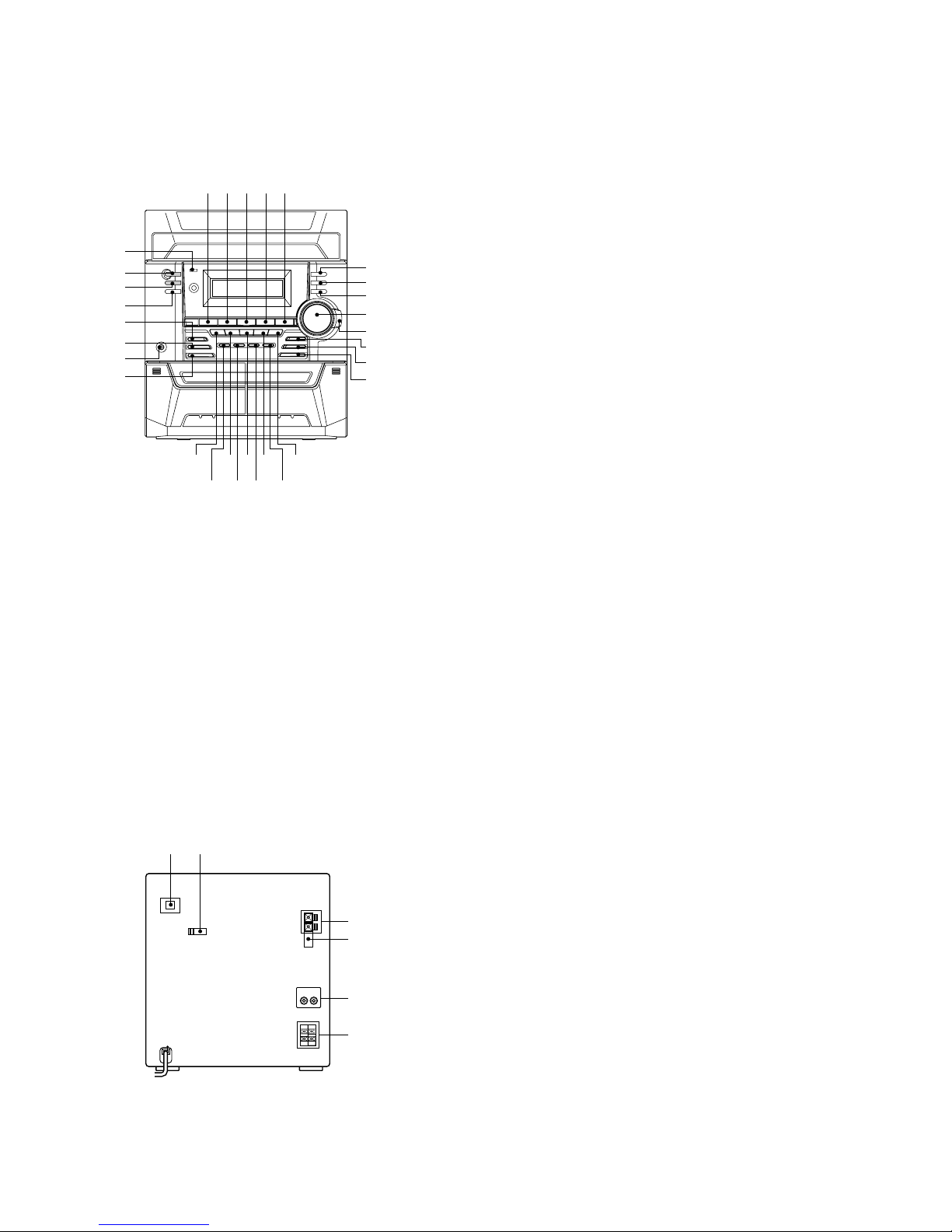
Location of Controls ....................................................... 4
Setting the Time .............................................................. 5
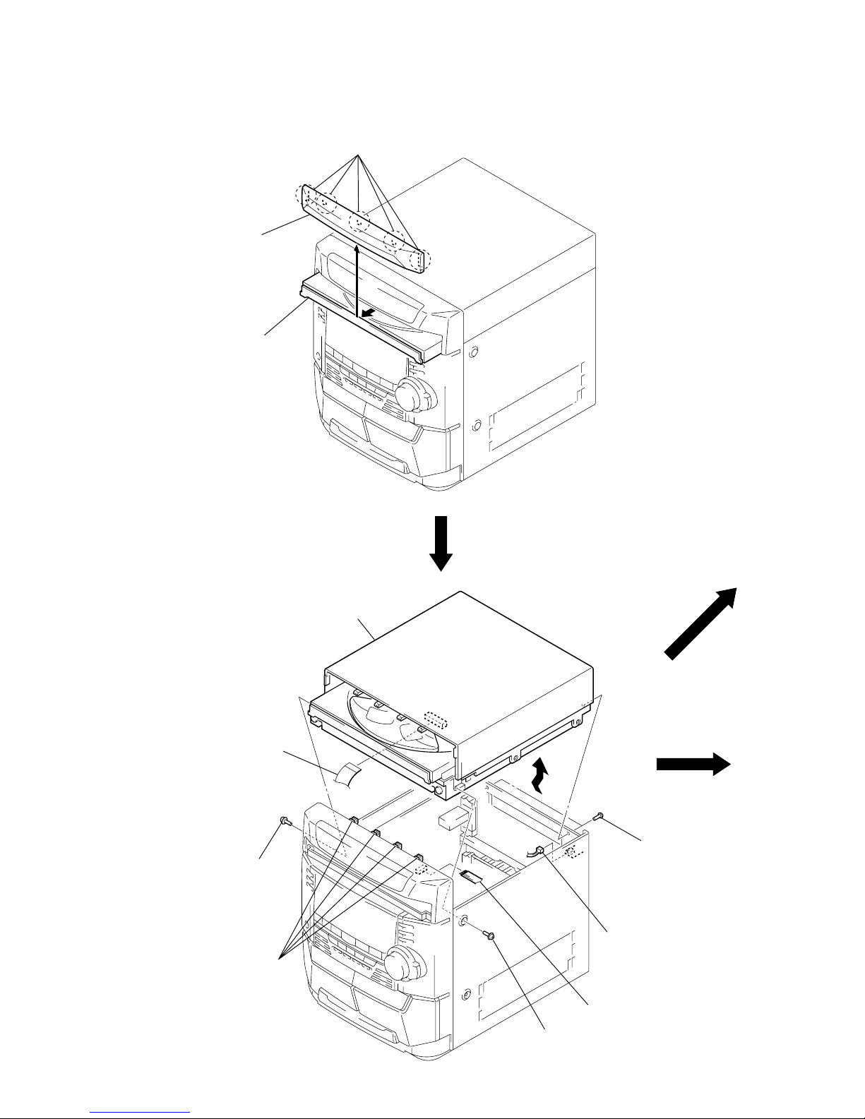
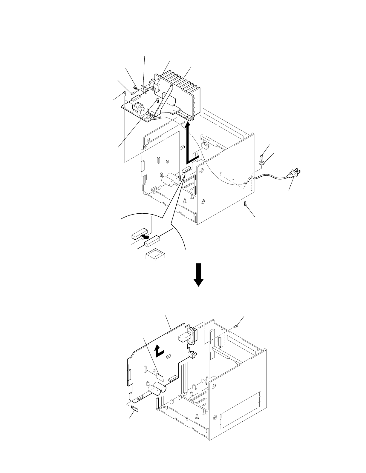
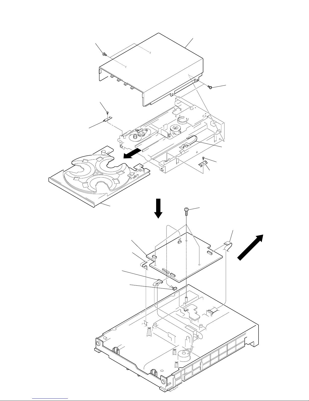
3. DISASSEMBLY ......................................................... 6
4. DIAGRAMS
4-1. Note for Printed Wiring Boards and
Schematic Diagrams ....................................................... 13
4-2. Schematic Diagram – CD Section (1/4) – ..................... 14
4-3. Schematic Diagram – CD Section (2/4) – ..................... 15
4-4. Schematic Diagram – CD Section (3/4) – ..................... 16
4-5. Schematic Diagram – CD Section (4/4) – ..................... 17
4-6. Printed Wiring Boards – CD Section – ......................... 18
4-7. Printed Wiring Boards – MAIN/TR Boards –............... 19
4-8. Schematic Diagram – MAIN Board (1/4) – .................. 20
4-9. Schematic Diagram – MAIN Board (2/4) – .................. 21
4-10. Schematic Diagram – MAIN Board (3/4) – .................. 22
4-11. Schematic Diagram
– MAIN (4/4)/TR Boards – ............................................ 23
4-12. Schematic Diagram – PANEL Section (1/3) – .............. 24
4-13. Schematic Diagram – PANEL Section (2/3) – .............. 25
4-14. Schematic Diagram – PANEL Section (3/3) – .............. 26
4-15. Printed Wiring Board – PANEL Section – .................... 27
4-16. Printed Wiring Board – AMP Board
(US, Canadian, AEP, UK, Australian models) – ............ 28
4-17. Schematic Diagram – AMP Board
(US, Canadian, AEP, UK, Australian models) – ............ 29
4-18. Printed Wiring Boards
– AMP (E model)/AC/FUSE Boards – ........................... 30
4-19. Schematic Diagram
– AMP (E model)/AC/FUSE Boards –........................... 31
5. EXPLODED VIEWS................................................ 37
6. ELECTRICAL PARTS LIST ............................... 43
General
Po er requirements
North American model: 120 V AC, 60 Hz
European model: 230 V AC, 50/60 Hz
Australian model: 220 – 240 V AC, 50/60 Hz
Mexican model: 120 V AC, 50/60 Hz
Other models: 110 – 120 V or 220 – 240 V
AC, 50/60 Hz
Adjustable ith voltage
selector
Po er consumption
U.S.A. model: 110 atts
Canadian model: 120 atts
European model: 105 atts
Other model: 120 atts
Dimensions ( /h/d)
Approx. 280 x 325 x 418 mm
Mass
U.S.A. model: Approx. 8.1 kg
Canadian model: Approx. 8.1 kg
European model: Approx. 8.2 kg
Other model: Approx. 8.3 kg
Supplied accessories: AM loop antenna (1)
FM lead antenna (1)
Remote Commander (1)
Design and specifications are subject to change
ithout notice.
CAUTION
Use of controls or adjustments or performance of procedures
other than those specified herein may result in hazardous ra-
diation exposure.
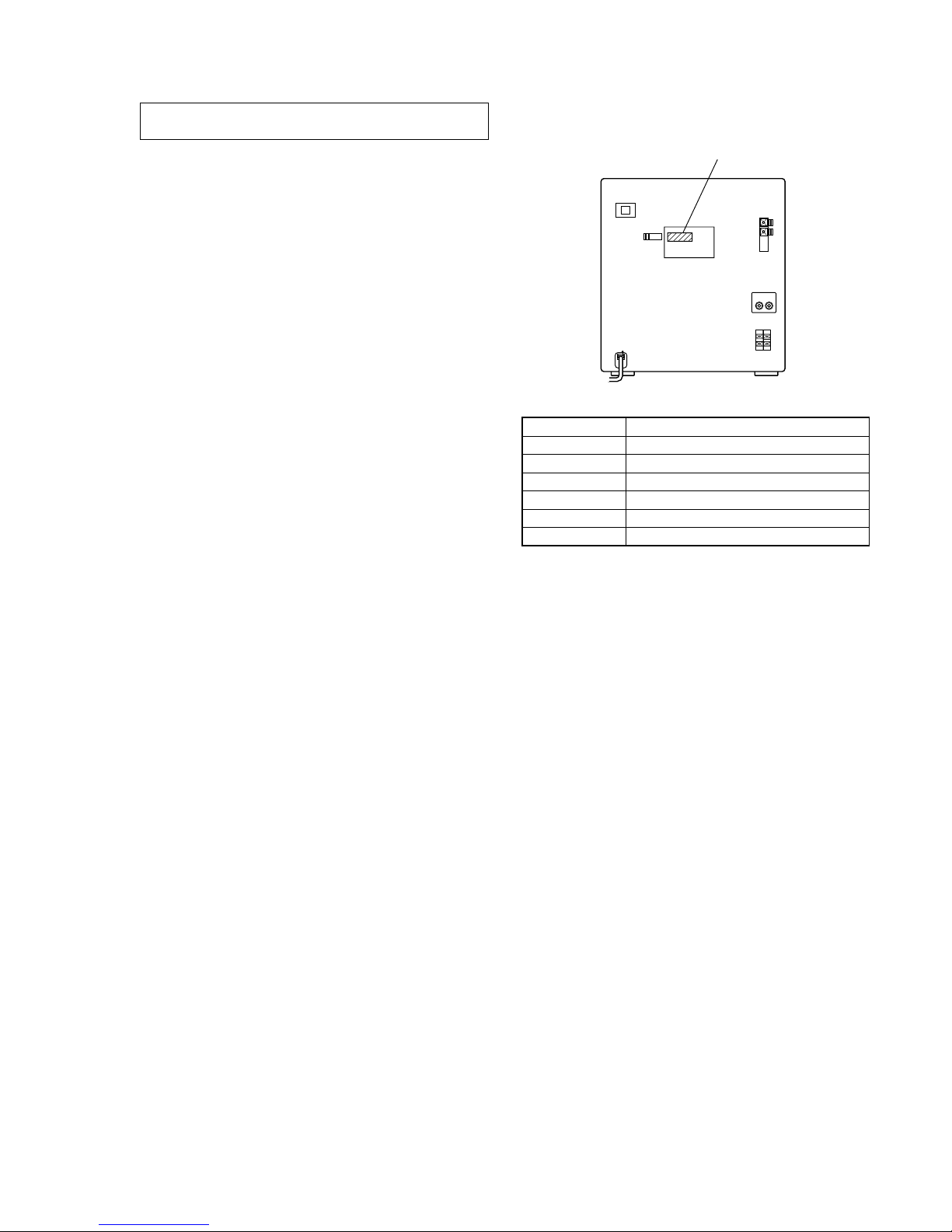
This appliance is classified as a CLASS 1 LASER product.
The CLASS 1 LASER PRODUCT MARKING is located on
the rear exterior.

3
SECTION 1
SERVICING NOTES
The laser diode in the optical pick-up block may suffer electro-
static break-down because of the potential difference generated
by the charged electrostatic load, etc. on clothing and the human
body.
During repair, pay attention to electrostatic break-down and also
use the procedure in the printed matter which is included in the
repair parts.
The flexible board is easily damaged and should be handled with
care.
NOTES ON LASER DIODE EMISSION CHECK
The laser beam on this model is concentrated so as to be focused
on the disc reflective surface by the objective lens in the optical
pick-up block. Therefore, when checking the laser diode emis-
sion, observe from more than 30 cm away from the objective lens.
Notes on chip component replacement
• Never reuse a disconnected chip component.
• Notice that the minus side of a tantalum capacitor may be dam-
aged by heat.
Flexible Circuit Board Repairing
• Keep the temperature of the soldering iron around 270 ˚C dur-
ing repairing.
• Do not touch the soldering iron on the same conductor of the
circuit board (within 3 times).
• Be careful not to apply force on the conductor when soldering
or unsoldering.
NOTES ON HANDLING THE OPTICAL PICK-UP
BLOCK OR BASE UNIT
• MODEL IDENTIFICATION
– Rear Panel –
Power Voltage Indication
Model Power Voltage Indication
US model AC: 120 V -60 Hz 110 W
Canadian model AC: 120 V -60 Hz 120 W
AEP, UK models AC: 230 V -50/60 Hz 105 W
Australian model AC: 220 – 240 V -50/60 Hz 120 W
Mexican model AC: 110 – 120 V -50/60 Hz 120 W
Other models AC: 110 – 120 V/220 – 240 V -50/60 Hz 120W

4
SECTION 2
GENERAL
• LOCATION OF CONTROLS
– FrontView –
– Rear View –
1TIMER indicator
2STANDBY ?/1button and indicator
3DISPLAY button
4SPECTRUM button
5GROOVE button and indicator
6FILE SELECT button
7PHONES jack
8ENTER button
9– .button
0xbutton
qa gGbutton and indicator
qs Xbutton
qd >+ button
qf PLAY MODE, DIRECTION button
qg REPEAT, STEREO/MONO button
qh EDIT, TUNER MEMORY button
qj VOLUME knob
qk jJbutton
ql REC button and indicator
w; REC PAUSE button and indicator
wa CD SYNC button
ws DISC SKIP EX-CHANGE button
wd MD button and indicator
wf DISC 1 button
wg TAPE A/B button and indicator
wh DISC 2 button
wj CD button and indicator
wk DISC 3 button
wl TUNER/BAND button and indicator
e; ZOPEN/CLOSE button
1CD DIGITAL OUTPUT (OPTICAL) connector
2VOLTAGE SELECTOR switch (E model)
3AM ANTENNA terminals
4FM ANTENNA jack or terminals
5MD IN jacks
6SPEAKER terminals
1
5
6
8
7
2qf
qh
ql
w;
wa
qk
qg
qj
9 0 qa qs qd
e;wk
wjwg wlwd
wfws wh
4
3
4
1 2
5
3
6

5
This section is extracted from
instruction manual.
1Press CLOCK/TIMER SET.
T e our indication flas es.
.
nN
Xx
mM
>
Step 2: Setting the
time
You must set t e time before using t e timer
functions.
T e clock uses a 24- our system on t e
European model, and a 12- our system on
ot er models.
T e 12- our system is used for illustration
purposes.
1
3,5
2,4
2Press . or > repeatedly to set
t e our.
3Press ENTER.
T e minute indication flas es.
4Press . or > repeatedly to set
t e minute.
5Press ENTER.
T e clock starts working.
Tip
If you make a mistake, start over from step 1.
To change the time
T e previous explanation s ows ow to set
t e time w ile t e power is off. To c ange t e
time w ile t e power is on, do t e following:
1Press CLOCK/TIMER SET.
2Press . or > repeatedly to select SET
CLOCK.
3Press ENTER.
4Perform steps 2 t roug 5 above.
Note
T e clock settings are canceled w en you disconnect
t e power cord or if a power failure occurs.

6
Note: Follow the disassembly procedure in the numerical order given.
SECTION 3
DISASSEMBLY
CD DOOR
CD ASS’Y
1Pull out the CD tray.
4Push the CD tray.
2five claws
3CD door
1screw
4four claws
6wire (flat type) (22core)
(CN705)
1screw
2two screw
s
3
8CD ass'y
7wire (6core)
(CN301)
5connector
(CN703)
CD TRAY (Page 10)

7
FRONT PANEL
6screw
2connector
1wire (flat type) (16core)
5three screws
6screw
CN601
3wire (flat type
)
(CN702)
4two rivets
2connector
(CN201)
8front panel section
7two claws
MECH DECK (CWL-44-FR)
1six screws
2harnes
s
3mech deck (CWL-44-FR)

8
POWER TRANSFORMER (T001)
REAR COVER
2rear cover
1eight screws
1screw
1two screws
1four screws
3four screws
4power transformer (T001
)
1Remove two solders.
2connector
(CN803)

9
AMP BOARD
0connector
(CN701)
9two screws
5screw
6harness qa AMP board
9screw
8TR board
7bracket
3AC cord washe
r
4power cord
1three screws
2screw
MAIN BOARD
3two screws
2wire (flat type) (16core)
(CN501)
1flat cable
(CN804)
4MAIN board

10
CD TRAY
1two screws
2top cabinet
1two screws
4screw
6screw
7bracket
5bracket
8CD tray
3wire (flat type) (5core
)
(CN06)
DECODE BOARD
4three screws
6DECODE board
1wire (flat type) (5core)
(CN706)
2wire (flat type) (15core)
(CN701)
3connector
(CN707)
5connector
(CN702)

11
BASE UNIT
2screw
3UD-gear
4screw
5UD-cam
8spring
7spring
6spring
1two screw
s
9base unit
CASSETTE LID
cassette door
(Note: Four claws are used.)

12
MEMO

1313
SECTION 4
DIAGRAMS
4-1. NOTE FOR PRINTED WIRING BOARDS AND SCHEMATIC DIAGRAMS
• Circuit Boards Location
Note on PrintedWiring Board:
•Y: parts extracted from the conductor side.
•b: Pattern from the side which enables seeing.
(The other layers' patterns are not indicated.)
Note on Schematic Diagram:
• All capacitors are in µF unless otherwise noted. U: µF,
pF: µµF 50 WV or less are not indicated except for
electrolytics and tantalums.
• If a numeric value of capacitor is a decimal fraction, the
preceding zero may be omitted.
(For example, .1 expresses 0.1)
• All resistors are in Ωand 1/4W or less unless otherwise
specified.
•5: fusible resistor.
•3: printed resistor.
•C: panel designation.
•U: B+ Line.
•V: B– Line.
•H: adjustment for repair.
• Voltages are taken withaVOM(Input impedance 10 MΩ).
Voltage variations may be noted due to normal produc-
tion tolerances.
• Waveforms are taken with a oscilloscope.
Voltage variations may be noted due to normal produc-
tion tolerances.
• Circled numbers refer to waveforms.
• Signal path.
F: FM
f: AM
E: TAPE PLAY (DECK A)
d: TAPE PLAY (DECK B)
G: TAPE REC
J: CD PLAY (ANALOG OUT)
c: CD PLAY (DIGITAL OUT)
• Abbreviation
AUS : Australian model
CND : Canadian model
Note:
The components identi-
fied by mark 0or dotted
linewithmark 0are criti-
cal for safety.
Replace only with part
number specified.
Note:
Lescomposants identifiés par
une marque 0sont critiques
pour la sécurité.
Ne les remplacer que par une
pièce portant le numéro
spécifié.
SW C board
SW D board
SW B board
DECODE board
MOTOR boar
d
SW A board
MAIN board
SENSOR board
FRONT board
H/P board
AMP board
SOCKET board
TR board

1414
HCD-BX2/DX2/DX2B
4-2. SCHEMATIC DIAGRAM – CD Section (1/4) – • See page 32 for Waveforms. •See page 32 for IC Block Diagrams.
• Voltages and waveforms are dc with respect to ground
under no-signal conditions.
no mark : CD PLAY
The components identified by mark 0or dotted
line with mark 0are critical for safety.
Replaceonly with part numberspecified.
Lescomposantsidentifiés par une marque 0sont
critiques pour la sécurité. Ne les remplacer que
par une pièce portant le numéro spécifié.
(Page 15)
(Page 16)

1515
HCD-BX2/DX2/DX2B
4-3. SCHEMATIC DIAGRAM – CD Section (2/4) –
• Voltages are dc with respect to ground under no-signal
conditions.
no mark : CD PLAY
(Page 17)
(Page
14)
(Page 25)
(Page 20)

1616
HCD-BX2/DX2/DX2B
4-4. SCHEMATIC DIAGRAM – CD Section (3/4) –
• Voltages are dc with respect to ground under no-signal
conditions.
no mark : CD PLAY
(Page 17)
(Page 14)

1717
HCD-BX2/DX2/DX2B
4-5. SCHEMATIC DIAGRAM – CD Section (4/4) – • See page 32 forWaveforms. •See page 32 for IC Block Diagrams.
• Voltages and waveforms are dc with respect to ground
under no-signal conditions.
no mark : CD PLAY
(Page 16)
(Page 15)

1818
HCD-BX2/DX2/DX2B
4-6. PRINTED WIRING BOARDS – CD Section – • See page 13 for Circuit Boards Location.
• Semiconductor
Location
Ref. No. Location
D703 G-7
D706 F-6
IC701 H-9
IC702 E-10
IC703 I-6
IC704 F-7
Q701 I-8
Q704 F-6
Q712 F-6
PH701 D-11
(Page 19)
(TO FRONT BOARD)

1919
HCD-BX2/DX2/DX2B
4-7. PRINTED WIRING BOARDS – MAIN/TR Boards – • See page 13 for Circuit Boards Location.
• Semiconductor
Location
Ref. No. Location
D101 E-3
D102 E-3
D103 B-3
D104 B-3
D109 D-6
D110 B-8
D111 A-9
D201 E-10
D202 D-9
D203 D-13
D301 F-14
D302 C-10
D303 F-5
D304 G-5
D305 G-6
D306 G-7
D307 D-12
D501 E-12
D502 B-12
D551 C-14
D552 C-13
D801 I-12
D804 I-14
D805 I-13
D806 I-14
D807 I-14
D808 I-14
D809 H-13
D811 H-14
D812 G-13
D813 H-15
D814 H-11
D816 G-14
IC101 B-11
IC102 B-6
IC103 D-4
IC201 F-9
IC301 F-4
IC302 G-7
IC501 C-13
IC502 E-13
Q101 B-5
Q108 A-4
Q114 D-4
Q116 C-8
Q117 B-8
Q201 G-10
Q202 F-11
Q203 G-10
Q204 E-11
Q205 G-10
Q206 E-11
Q207 E-9
Q208 D-9
Q209 E-9
Q213 G-9
Q214 F-8
Q251 D-10
Q252 D-10
Q253 B-12
Q305 G-6
Q306 F-6
Q308 C-10
Q309 F-6
Q501 B-12
Q502 B-12
Q503 B-13
Q504 B-13
Q505 B-13
Q506 B-13
Q551 F-13
Q552 F-13
Q801 H-4
Q802 I-4
Q803 I-15
Q804 I-14
Q805 G-14
(Page 28: US, CND, AEP, UK AUS models)
(Page 30: E model) (Page 18)
(Page 28: US, CND, AEP, UK AUS models)
(Page 30: E model)
(TO FRONT
BOARD)

2020
HCD-BX2/DX2/DX2B
4-8. SCHEMATIC DIAGRAM – MAIN Board (1/4) – • See page 32 forWaveforms.
• Voltages and waveforms are dc with respect to ground
under no-signal (detuned) conditions.
no mark : FM
( ) : AM
(Page 15)
(Page 22)
(Page
21)
(Page
23)
This manual suits for next models
3
Table of contents
Other Sony Stereo System manuals

Sony
Sony CMTBX1 - CMT BX1 Micro System User manual

Sony
Sony BKSR-2020 User manual

Sony
Sony SRS-BTS50 Parts list manual

Sony
Sony ZS ZS-SN10L User manual

Sony
Sony MEX-BT3100P User manual

Sony
Sony HCD-V8800 User manual

Sony
Sony LBT-D109CD User manual

Sony
Sony Psyc ZS-YN7 User manual

Sony
Sony CX-LFA500 User manual

Sony
Sony CX-JN1 User manual

Sony
Sony LBT-XG60 User manual

Sony
Sony MHC-V42D User manual

Sony
Sony MHC-771 - Mini Hi-fi Component System User manual

Sony
Sony CMT-SPZ50 User manual

Sony
Sony CMT-SBT40D User manual

Sony
Sony XDR-DS16iPN User manual

Sony
Sony CMT-DC1 User manual

Sony
Sony ZS-D5 User manual

Sony
Sony MHC-V83D User manual

Sony
Sony HCD-RXD6AV User manual