Sony ZS-PS30CP User manual

SERVICE MANUAL
Sony Corporation
Published by Sony Techno Create Corporation
ZS-PS30CP
SPECIFICATIONS
PERSONAL AUDIO SYSTEM
9-893-461-02
2012I33-1
© 2012.09
E Model
Ver. 1.1 2012.09
Model Name Using Similar Optical Pick-up Block CFD-S07CP
Optical Pick-up Block Name DA11MMVGP
CD player section
System
Compact disc digital audio system
Laser diode properties
Emission duration: Continuous
Laser output: Less than 44.6 μW
(This output is the value measured at a distance of
about 200 mm from the objective lens surface on the
optical pick-up block with 7 mm aperture.)
Number of channels
2
Frequency response
20 Hz - 20,000 Hz +1/–2 dB
Wow and utter
Below measurable limit
Radio section
Chilean, Peruvian, Asian and Argentina models
Frequency range
FM: 87.5 MHz - 108 MHz (50 kHz/100 kHz step)
AM: 531 kHz - 1,602 kHz (9 kHz step)
530 kHz - 1,610 kHz (10 kHz step)
Antennas
FM: Telescopic antenna
AM: Built-in ferrite bar antenna
USB section
Supported bit rate
MP3 (MPEG 1 Audio Layer-3):
32 kbps - 320 kbps, VBR
Sampling frequencies
MP3 (MPEG 1 Audio Layer-3):
32/44.1/48 kHz
(USB) port
USB-A (Full Speed)
General
Speaker
Full range: 8 cm dia., 8 Ω, cone type (2)
Outputs
Headphones jack (stereo minijack):
For 16 Ω - 32 Ω impedance headphones
Input
AUDIO IN jack (stereo minijack)
(USB) port: Type A, maximum current 500 mA
Power output
1.0 W + 1.0 W (at 8 Ω, 10% harmonic distortion)
Power requirements
For CD radio:
Chilean and Peruvian models: 230 V AC, 50 Hz
Asian model: 230 V AC - 240 V AC, 50 Hz
Panamanian and Taiwan models: 120 V AC, 60 Hz
Argentina model: 220 V - 230 V AC, 50 Hz
9 V DC, 6 R14 (size C) batteries (Except Argentina model)
Power consumption
AC 11 W
Battery life* (Except Argentina model)
For CD radio:
FM reception
R14P: approx. 7 h
Sony alkaline LR14: approx. 30 h
CD playback
R14P: approx. 1.5 h
Sony alkaline LR14: approx. 13 h
Dimensions
Approx. 299 mm × 126 mm × 210 mm (w/h/d)
(incl. projecting parts)
Mass
Approx. 2.4 kg (incl. batteries) (Except Argentina model)
Approx. 2 kg (Argentina model)
Supplied accessories
AC power cord (1)
*Battery life is subject to changes in surrounding temperature, usage
conditions, manufacture and battery type.
Design and specications are subject to change without notice.
Taiwan model
FM: 87.5 MHz - 108 MHz
AM: 531 kHz - 1,602 kHz
Panamanian model
FM: 87.5 MHz - 108 MHz
AM: 530 kHz - 1,710 kHz

ZS-PS30CP
2
1. SERVICING NOTES ............................................. 3
2. DISASSEMBLY
2-1. Disassembly Flow........................................................... 5
2-2. Battery Case Lid Block (Argentina model) .................... 5
2-3. Cabinet (Rear) Assy, Fuse (F901, F902)......................... 6
2-4. VOL Board...................................................................... 7
2-5. Cabinet (Front) Assy....................................................... 8
2-6. MAIN Board Block ........................................................ 9
2-7. MAIN Board ................................................................... 10
2-8. CD Block Assy................................................................ 11
2-9. Optical Pick-up (DA11MMVGP) (OP1) ........................ 11
2-10. CD Spring ....................................................................... 12
2-11. JACK (IN) Board............................................................ 12
2-12. Speaker (7.7 cm) (L-CH) (SP101).................................. 13
2-13. BUTTON (VOL) Board.................................................. 13
2-14. USB JACK Board........................................................... 14
2-15. Speaker (7.7 cm) (R-CH) (SP201).................................. 15
2-16. Telescopic Antenna (ANT1), Antenna Spring ................ 15
2-17. POWER Board................................................................ 16
3. TEST MODE ............................................................ 17
4. ELECTRICAL CHECKS ...................................... 18
5. DIAGRAMS
5-1. Block Diagram - MAIN Section -................................... 19
5-2. Block Diagram
- PANEL/POWER SUPPLY Section -............................ 20
5-3. Schematic Diagram - MAIN Section (1/2) -................... 22
5-4. Schematic Diagram - MAIN Section (2/2) -................... 23
5-5. Printed Wiring Board - MAIN Board -........................... 24
5-6. Printed Wiring Boards - MOTOR/PANEL Section - ...... 25
5-7. Printed Wiring Boards
- AUDIO/POWER SUPPLY Section -............................ 26
5-8. Schematic Diagram
- AUDIO/POWER SUPPLY Section -............................ 27
6. EXPLODED VIEWS
6-1. Overall Section ............................................................... 33
6-2. Main Section ................................................................... 34
6-3. Cabinet (Front) Section................................................... 35
6-4. Cabinet (Upper) Section ................................................. 36
6-5. CD Block Section ........................................................... 37
6-6. MAIN Board Section ...................................................... 38
6-7. Cabinet (Rear) Section.................................................... 39
7. ELECTRICAL PARTS LIST .............................. 40
Accessories are given in the last of the electrical parts list.
TABLE OF CONTENTS
NOTES ON CHIP COMPONENT REPLACEMENT
• Never reuse a disconnected chip component.
• Notice that the minus side of a tantalum capacitor may be dam-
aged by heat.
SAFETY-RELATED COMPONENT WARNING!
COMPONENTS IDENTIFIED BY MARK 0OR DOTTED LINE
WITH MARK 0ON THE SCHEMATIC DIAGRAMS AND IN
THE PARTS LIST ARE CRITICAL TO SAFE OPERATION.
REPLACE THESE COMPONENTS WITH SONY PARTS
WHOSE PART NUMBERS APPEAR AS SHOWN IN THIS
MANUAL OR IN SUPPLEMENTS PUBLISHED BY SONY.
CAUTION
Use of controls or adjustments or performance of procedures
other than those specified herein may result in hazardous radia-
tion exposure.
MPEG Layer-3 audio coding technology and patents
licensed from Fraunhofer IIS and Thomson.
Ver. 1.1

ZS-PS30CP
3
SECTION 1
SERVICING NOTES
UNLEADED SOLDER
Boards requiring use of unleaded solder are printed with the lead-
free mark (LF) indicating the solder contains no lead.
(Caution: Some printed circuit boards may not come printed with
the lead free mark due to their particular size)
: LEAD FREE MARK
Unleaded solder has the following characteristics.
• Unleaded solder melts at a temperature about 40 °C higher
than ordinary solder.
Ordinary soldering irons can be used but the iron tip has to be
applied to the solder joint for a slightly longer time.
Soldering irons using a temperature regulator should be set to
about 350 °C.
Caution: The printed pattern (copper foil) may peel away if
the heated tip is applied for too long, so be careful!
• Strong viscosity
Unleaded solder is more viscous (sticky, less prone to flow)
than ordinary solder so use caution not to let solder bridges
occur such as on IC pins, etc.
• Usable with ordinary solder
It is best to use only unleaded solder but unleaded solder may
also be added to ordinary solder.
NOTES ON HANDLING THE OPTICAL PICK-UP
BLOCK OR BASE UNIT
The laser diode in the optical pick-up block may suffer electro-
static break-down because of the potential difference generated by
the charged electrostatic load, etc. on clothing and the human body.
During repair, pay attention to electrostatic break-down and also
use the procedure in the printed matter which is included in the
repair parts.
The flexible board is easily damaged and should be handled with
care.
NOTES ON LASER DIODE EMISSION CHECK
The laser beam on this model is concentrated so as to be focused
on the disc reflective surface by the objective lens in the optical
pickup block. Therefore, when checking the laser diode emission,
observe from more than 30 cm away from the objective lens.
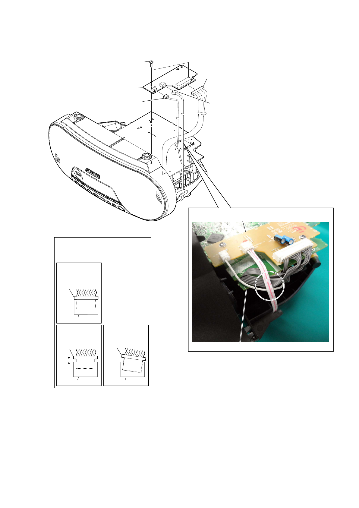
NOTE OF REPLACING THE IC1 ON THE MAIN BOARD
IC1 on the MAIN board cannot exchange with single. When this
part is damaged, exchange the complete mounted board.
TEST DISCS
Use following TEST DISC when this unit confirms the operation
and checks it.
Part No. Description
3-702-101-01 DISC (YEDS-18), TEST (for CD)
4-225-203-01 DISC (PATD-012), TEST (for CD)
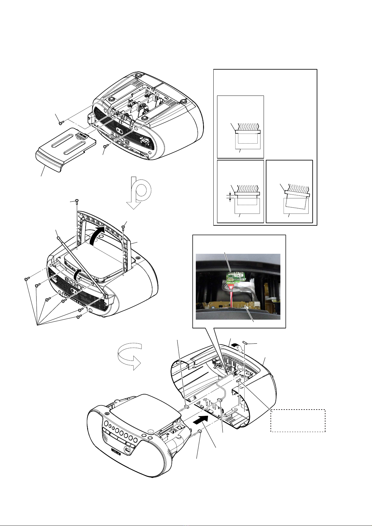
CHUCK PLATE JIG ON REPAIRING
On repairing CD section, playing a disc without the CD lid, use
CHUCK PLATE JIG.
Part No. Description
X-4918-255-1 CHUCK PLATE JIG
LASER DIODE AND FOCUS SEARCH OPERATION
CHECK
During normal operation of the equipment, emission of the laser
diode is prohibited unless the upper lid is closed while turning on
the S801 (push switch type).
The following checking method for the laser diode is operable.
• Method
Emission of the laser diode is visually checked.
1. Open the CD lid.
2. In the standby state, press the [POWER] button to turn the
power on.
3. Press the [CD] button to turn the CD function.
4. Push the S801 as shown in Fig.1.
Note: Do not push the detection lever strongly, or it may be bent or
damaged.
5. Check the object lens for confirming normal emission of the
laser diode. If not emitting, there is a trouble in the automatic
power control circuit or the optical pick-up.
In this operation, the object lens will move up and down 2
times along with inward motion for the focus search.
S801
Fig. 1. Method to push the S801

ZS-PS30CP
5
SECTION 2
DISASSEMBLY
• This set can be disassembled in the order shown below.
2-1. DISASSEMBLY FLOW
(Argentina)
SET
2-2. BATTERY CASE LID BLOCK (Argentina model)
(Page 5)
2-3. CABINET (REAR) ASSY, FUSE (F901, F902)
(Page 6)
2-4. VOL BOARD
(Page 7)
2-5. CABINET (FRONT) ASSY
(Page 8)
2-6. MAIN BOARD BLOCK
(Page 9)
2-12. SPEAKER (7.7 cm)
(L-CH) (SP101)
(Page 13)
2-7. MAIN BOARD
(Page 10)
2-8. CD BLOCK ASSY
(Page 11)
2-11. JACK (IN) BOARD
(Page 12)
2-16. TELESCOPIC ANTENNA (ANT1),
ANTENNA SPRING
(Page 15)
2-17. POWER BOARD
(Page 16)
2-15. SPEAKER (7.7 cm)
(R-CH) (SP201)
(Page 15)
2-13. BUTTON (VOL) BOARD
(Page 13)
2-14. USB JACK BOARD
(Page 14)
2-10. CD SPRING
(Page 12)
2-9. OPTICAL PICK-UP
(DA11MMVGP) (OP1)
(Page 11)
Ver. 1.1
Note: Follow the disassembly procedure in the numerical order given.
2-2. BATTERY CASE LID BLOCK (Argentina model)
– Rear bottom side view –
3battery case lid block
2Pushing Aportion with a finger, flat-head screwdriver is pushed down
in the direction of the arrow and battery case lid block is removed.
1Insert a flat-head screwdriver into a recess
in the bottom of the unit.
Note: Please twist a filament tape at the tip
of flat-head screwdriver.
A

ZS-PS30CP
6
2-3. CABINET (REAR) ASSY, FUSE (F901, F902)
3Lift up the hundle.
(EXCEPT Argentina)
– Rear side view –
– Rear bottom side view –
4Lift up the telescopic
antenna.
1battery case lid block
0connector
(CN983)
9connector
(CN304)
8connector
(CN301)
6Push down the handle.
2two tapping screws
(BV B2.6)
5six tapping screws
(BV B2.6)
2tapping screw
(BV B2.6)
5tapping screw
(BV B2.6)
5tapping screw
(BV B2.6)
7Remove the cabinet (rear) assy
in the direction of an arrow.
qa cabinet (rear) assy
MAIN board
HP JACK board
Insert is shallow
Insert is straight
to the interior.
connector
Insert is incline
connector
connector connector
connector connector
NG
OK
NG
:LUHVHWWLQJ
qs fuse (F901)
qd fuse (F902)
Note 2: When you install the connector, please
install them correctly.
There is a possibility that this machine
damages when not correctly installing it.
Note 1: Refer to 2-2 for Argentina model.
Ver. 1.1

ZS-PS30CP
7
2-4. VOL BOARD
5VOL board
VOL board
MAIN board
– Bottom side view –
:iUe settiQJ
1connector
(CN302)
3connector
(CN305)
2connector
(CN306)
4two tapping screws
(BV B2.6)
Insert is shallow
Insert is straight
to the interior.
connector
Insert is incline
connector
connector connector
connector connector
NG
OK
NG
Note: When you install the connector, please
install them correctly.
There is a possibility that this machine
damages when not correctly installing it.

ZS-PS30CP
8
2-5. CABINET (FRONT) ASSY
:LUHVHWWLQJ
–5HDUULJKWVLGHYLHZ–
4two tapping screws
(BV B2.6)
6cabinet (front) assy
MAIN board
1connector
(CN801)
2connector
(CN905)
3connector
(CN1001)
4two tapping screw
s
(BV B2.6)
5two claws
Insert is shallow
Insert is straight
to the interior.
connector
Insert is incline
connector
connector connector
connector connector
NG
OK
NG
Note: When you install the connector, please
install them correctly.
There is a possibility that this machine
damages when not correctly installing it.
tape
:LUHVHWWLQJ
MAIN board
wire from BUTTON (MAIN) board
wire from USB JACK board
speaker wire
speaker wire
heat sink (AMP)
tape
tape CN801 CN311 CN240
C329
MAIN board
heat sink (AMP)
C329
C950
CN905

ZS-PS30CP
9
2-6. MAIN BOARD BLOCK
Note 1: Before disconnecting the flexible flat cable (16 core) of optical pick-up block, solder the short-land.
6Solder the short-land.
Note 2: When assembling the MAIN
board block, remove the
solder of short-land after
connecting the flexible flat
cable (16 core).
cabinet (upper)
7flexible flat cable (16 core)
8flexible flat cable (6 core)
9MAIN board block
MAIN board
front side
tape
3connector
(S801)
4two tapping screws
(BV B2.6)
4four tapping screws
(BV B2.6)
4tapping screw
(BV B2.6)
1tapping screw
(PWH B2.6)
2Remove ferrite core
from rib.
ferrite core
Wire is below a screw hole. Wire is above a screw hole.
ferrite core
5Remove the MAIN board block
in the direction of an arrow.
– Cabinet (upper) block bottom side view –
OK NG
tape
:ire settinJNote 3: When installing the flexible
flat cable, ensure the coloured
line.
No slanting after insertion.
coloured line
coloured line
Insert is straight to the interior.
Insert is incline
flexible flat
cable
flexible flat
cable
connector
connector
OK
NG

ZS-PS30CP
10
2-7. MAIN BOARD
1ferrite core (FC1)
3two cabinet upper
cushions 10 X 7 X0.3
3two cabinet upper
cushions 10 X 7 X0.3
2flexible flat cable (16 core) (FFC801)
(CN810)
flexible flat cable
(16 core)
(FFC801)
)HUULWHFRUH)&VHWWLQJ
WireVeWWiQJ
ferrite core (FC1)
tape
Be based on
a black line.
Roll the wire three times.
from MAIN board
to POWER board
5two tapping screws
(BV B2.6)
qd holder (LCD) block
qs screw
qs screw
6two bosses (PC board)
qa liquid crystal display
panel (LCD401)
0Remove adhesive
sheet (panel dock).
9Remove thirty
three solders.
7Remove two solders.
qh Remove two solders.
qk MAIN board
MAIN board
qj heat sink (AMP)
qf Remove three solders.
qg shield plate
C703
tape
tape
C919
CN808
C808
X802 C821 Q905
8led (D401)
4cushion
(CAB rear)
coloured line
coloured line
Insert is straight to the interior.
Insert is incline
flexible flat
cable
flexible flat
cable
connector
connector
OK
NG
Note: When installing the flexible flat
cable, ensure the coloured line.
No slanting after insertion.

ZS-PS30CP
11
2-9. OPTICAL PICK-UP (DA11MMVGP) (OP1)
2-8. CD BLOCK ASSY
2CD block assy
– Cabinet (upper) block bottom side view –
1two tapping screw
s
(PWH B2.6)
1two tapping screws
(PWH B2.6)
3claw
2vibration proof rubber
(green)
1vibration proof rubber
(red)
3claw
3claw
1vibration proof rubber
(red)
7optical pick-up (DA11MMVGP)
(OP1)
optical pick-up
(DA11MMVGP)
(OP1)
6MOTOR board
4CD cover
Note: Three claws might be fixed by bond.
When installing the CD cover, please
fix three claws using the following bond.
Part No. Description
7-432-912-48 SONY BOND SC608LV (180 ml)
2vibration proof rubber
(green)
vibration proof rubber
Upper side
Lower side
5Remove four solders.
9LEUDWLRQSURRIUXEEHUVHWWLQJ
3claw

ZS-PS30CP
12
1Open the CD lid.
5CD spring
CD spring
4shaft
3claw
&'VSULQJVHWWLQJ
&'VSULQJVHWWLQJ
CD lid
2Remove the spring
(CD) from the ditch
of CD lid.
ditch
CD spring
CD lid
OK NG
1Insert the CD spring.
4Insert the CD spring
to the ditch of CD lid.
2Insert in the shaft.
$VVHPEOLQJSURFHGXUHRIWKH&'VSULQJ
3Hook CD spring on claw.
–&DELQHWXSSHUEORFN–
ULJKWVLGHYLHZ
2-11. JACK (IN) BOARD
2-10. CD SPRING
1tapping screw
(BV B2.6)
2JACK (IN) board
– Cabinet (front) block rear right side view –

ZS-PS30CP
13
2-13. BUTTON (VOL) BOARD
2-12. SPEAKER (7.7 cm) (L-CH) (SP101)
4speaker (7.7 cm)
(L-CH) (SP101)
2Remove the speaker (7.7 cm) (L-CH)
(SP101) in the direction of an arrow.
– Cabinet (front) block rear right side view –
1four tapping screws
(BV B2.6)
red (+)
white (−)
3Remove solder
from the
“−” terminal.
3Remove solder
from the
“+” terminal.
:ire setting
speaker terminal Twist a wire around
a speaker terminal hole.
wire
Speaker (7.7 cm) (L-CH) (SP101) setting
Install the speaker
(7.7 cm) (L-CH)
(SP101) in inside
two ribs.
1two tapping screws
(BV B2.6)
2RETAINER board
4connector
(CN402)
3Remove the BUTTON (VOL) board
block in the direction of an arrow.
7BUTTON (VOL) board
5button (volume)
6two sheets (1)
Insert is shallow
Insert is straight
to the interior.
connector
Insert is incline
connector connector connector
connector connector
NGOK NG
Note: When you install the connector, please install them correctly.
There is a possibility that this machine damages when not
correctly installing it.
– Cabinet (front) block rear left side view –

ZS-PS30CP
14
2-14. USB JACK BOARD
:LUHVHWWLQJ
3tapping screw
(BV B2.6)
3tapping screw
(BV B2.6)
1tapping screw
(PWH B2.6)
2Remove ferrite core from rib.
5ferrite core
(FC2)
6Remove four
solders.
7shield plate
(USB)
4Remove the USB JACK board block
in the direction of an arrow.
8USB JACK board
)HUULWHFRUH)&VHWWLQJ
ferrite core
(FC2)
Roll the wire twice.
tape
Be based on a red line.
USB JACK board
USB JACK board
BUTTON (VOL) board
speaker (7.7 cm) (L-CH) (SP101)
speaker (7.7 cm) (R-CH) (SP201)
tape
tape
tape
–&DELQHWIURQWEORFNUHDUOHIWVLGHYLHZ–

ZS-PS30CP
15
2-16. TELESCOPIC ANTENNA (ANT1), ANTENNA SPRING
2-15. SPEAKER (7.7 cm) (R-CH) (SP201)
4speaker (7.7 cm)
(R-CH) (SP201)
1four tapping screws
(BV B2.6)
2Remove the speaker (7.7 cm) (R-CH)
(SP201) in the direction of an arrow.
– Cabinet (front) block rear left side view –
red (+)
white (−)
3Remove solder
from the
“−” terminal.
3Remove solder
from the
“+” terminal.
:ire settinJ
Speaker (7.7 cm) (R-CH) (SP201) settinJ
speaker terminal Twist a wire around
a speaker terminal hole.
wire
Install the speaker (7.7 cm) (R-CH)
(SP201) in inside two ribs.
5antenna spring
antenna spring 2telescopic antenna
(ANT1)
1screw
(P M3)
4claw
$QWHQQDVSULQJVHWWLQJ
3tapping screw
(BV B2.6)
1
2
4
5
6
7
3
Note: Attach to numerical order.

ZS-PS30CP
16
2-17. POWER BOARD
1connector
(CN903)
7power transformer (T901)
8POWER board
:LUHVHWWLQJ
2two tapping screws
(BV B2.6)
2two tapping screws
(BV B2.6)
2tapping screw
(BV B2.6)
4tapping screw
(BV B2.6)
3Remove the POWER board block
in the direction of an arrow.
5holder (inlet)
ditch of rib Twist a wire 3 to 4 times.
Note: Arranging so that a wire may not exceed this line.
tape
tape tape
6Remove five solders.
white
red
Insert is straight
to the interior.
connector
connector
OK
Insert is shallow Insert is incline
connector connector
connector connector
NG NG
Note: When you install the connector, please install themcorrectly.
There is a possibility that this machine damages when not
correctly installing it.
–&DELQHWUHDUEORFNIURQWOHIWVLGHYLHZ–

ZS-PS30CP
17
SECTION 3
TEST MODE
EEPROM CLR
It can clear the EEPROM.
Procedure:
1. While pressing two buttons of [DISPLAY] and [>] simulta-
neously and connect the AC power cord.
2. The EEPROM is cleared, and the message “CLR” is displayed
on the liquid crystal display, then becomes the standby state.
PANEL AND KEY TEST
It can check the liquid crystal display and button.
Procedure:
1. While pressing two buttons of [x] and [DISPLAY] simultane-
ously and connect the AC power cord.
2. It enters the panel and key test mode, and all segments on the
liquid crystal display light up.
3. Each time a button is pressed, the segments on the liquid crys-
tal display corresponding to each button disappear.
4. When all buttons are pressed, all segments on the liquid crystal
display disappear.
5. When the [DISPLAY] button is pressed, becomes the standby
state.
Releasing method:
Disconnect the AC power cord.
CD TEST MODE
It can check the focus error and tracking error.
Procedure:
1. Connect the oscilloscope to TP895 (FEI) and TP814 (GND) on
the MAIN board.
+
–
MAIN board
TP895 (FEI)
TP814 (GND)
oscilloscope
2. Open the CD lid.
3. While pressing [x] button for around 8 seconds and connect
the AC power cord.
4. It enters the CD test mode, and the message “TEST 1” is dis-
played on the liquid crystal display.
5. When the message “TEST 1” is displayed on the liquid crystal
display, press the [u] button.
6. It enters the focus error test mode, and the message “FE” is
displayed on the liquid crystal display.
7. When the CD disc is placed and CD lid is closed, focus error
starts.
8. Confirm that oscilloscope waveform is as shown in the figure
below.
1.2 ± 0.6 Vp-p
VOLT/DIV: 200 m
V
TIME/DIV: 2 ms
9. Disconnect the AC power cord to release the focus error test
mode.
10. Connect the oscilloscope to TP805 (TEI) and TP814 (GND) on
the MAIN board.
+
–
MAIN board
TP805 (TEI)
TP814 (GND)
oscilloscope
11. Open the CD lid.
12. While pressing [x] button for around 8 seconds and connect
the AC power cord.
13. It enters the CD test mode, and the message “TEST 1” is dis-
played on the liquid crystal display.
14. When the [>] button is pressed, the message on the liquid
crystal display change to “TEST 2”.
(When the [>] button is pressed again, the message on the
liquid crystal display change to “TEST 1”)
15. It enters the tracking error test mode, and the message “TE” is
displayed on the liquid crystal display.
16. When the CD lid is closed, tracking error starts.
17. Confirm that oscilloscope waveform is as shown in the figure
below.
1.2 ± 0.6 Vp-p
VOLT/DIV: 500 m
V
TIME/DIV: 2 ms
Releasing method:
Press the [POWER] button or disconnect the AC power cord.
Connection Location:
– MAIN Board (Conductor Side) –
TP814
(GND)
TP895
(FEI)
TP805
(TEI)

ZS-PS30CP
18
SECTION 4
ELECTRICAL CHECKS
TUNER SECTION 0 dB = 1 V
[AM]
Setting:
Function: RADIO
Band: AM
AM RF signal
generator
30% amplitude
modulation by
400 Hz signal
Output level:
as low as possible
Put the lead-wire
antenna close to
the unit.
HP JACK board
ijack (J302)
unit +
í
level meter
32 :
[FM]
Setting:
Function: RADIO
Band: FM
FM RF signal
generator
75 kHz frequency
deviation by
1 kHz signal
Output level:
as low as possible
HP JACK board
ijack (J302)
unit
0.01PF+
í
level meter
MAIN board
TP814 (GND)
32 :
MAIN board
JW101
Note: Perform FM frequency coverage check after removing FM tele-
scopic antenna (ANT1).
no mark: Chilean, Peruvian, Asian, Taiwan and Argentina models
( ): Panamanian model
AM FREQUENCY COVERAGE CHECK
Check that reading on level meter is the maximum
Confirmation 531 (530) kHz
Confirmation 1,602 (1,710) kHz
FM FREQUENCY COVERAGE CHECK
Check that reading on level meter is the maximum
Confirmation 87.5 MHz
Confirmation 108 MHz
CD SECTION
Note:
1. CD block is basically constructed to operate without adjustment.
2. Use YEDS-18 disc (Part No. 3-702-101-01) unless otherwise indicat-
ed.
3. Use an oscilloscope with more than 10 Mimpedance.
4. Clean the object lens by an applicator with neutral detergent when the
signal level is low than specified value with the following checks.
5. Check the focus bias check when optical pick-up block is replaced.
FOCUS BIAS CHECK
+
–
MAIN board
TP804 (RF)
TP711
(
VREF
)
oscilloscope
Procedure:
1. Connect the oscilloscope to TP804 (RF) and TP711 (VREF)
on the MAIN board.
2. In the standby state, press the [POWER] button to turn the
power on.
3. Press the [CD] button to turn the CD function.
4. Set the disc (YEDS-18) and press the [u] button to playback.
5. Confirm that oscilloscope waveform is as shown in the figure
below. (eye pattern)
A good eye pattern means that the diamond shape () in the
center of the waveform can be clearly distinguished.
VOLT/DIV: 200 m
V
TIME/DIV: 500 ns
level: 1.5 Vp-p
Connection Location:
– MAIN Board (Conductor Side) –
TP814
(GND)
TP804
(RF)
TP711
(VREF)
JW101
Ver. 1.1

ZS-PS30CP
ZS-PS30CP
1919
OP1
OPTICAL PICK-UP BLOCK
(DA11MMVGP)
A
B
C
D
E
F
PD
LD
AUTOMATIC
POWER CONTROL
Q701
90 LDO
99 FOO
100 TR O
2DMO
1FMO
40 MOTOR-MUTE
FC+ 26 24
F+
FC– 27 F–
TR+ 18 T+
TR– 17 T–
12 SL+
11 SL–
2 SP+
1 SP–
86 TPI (F)
89 MDI
VC 88 VRO
87 TNI (E)
84 FPI2 (D)
82 FNI2 (C)
85 FPI1 (B)
83 FNI1 (A) 78 AGCI
R-CH
(FIN)
23VREF
79RFO 22LO
24RO
93USB DATA 35 USB DATA
92USB BCK
D+
D– 38 USB BCK
71LRCK 39 USB LRCK
D+
85
79
D–
80
73
USB RX 32 USB TX
84USB TX 31 USB RX
94USB GATE 17 USB GATE
96USB REQ 43 USB REQ
2USB PWR 55 USB PWR
1RST 45 USB RESET
20(TIN)
9(SLIN)
3SPIN
FOCUS/TRACKING COIL DRIVE,
SLED/SPINDLE MOTOR DRIVE
IC701
7
MUTE
USB CONTROLLER
IC1001
J1001
3
2
X1001
9MHz
X2
75
X1
CD DSP,
SYSTEM CONTROLLER
IC801 (1/2)
(SLED) M
(SPINDLE) M
FM/AM RECEIVER
IC1
6SCL
44A MUTE
5SDA
1INLCD
5INLAU
13 VOLIN L
9INLTU
INPUT SELECTOR, ELECTRICAL VOLUME
IC303
15 RST
17 SCLK
18 SDIO
23ROUT
24LOUT
12ICOUT L
19
X1
32.768kHz
RCLK
3
GPO3/
DCLK
27
X801
16.9344MHz
XI
28
XO
11
X802
4.19MHz
MXI
52
O-SHIFT2
10
MXO
: AUDIO IN
: CD PLAY
: FM
: AM
SIGNAL PATH
R-ch is omitted due to same as L-ch.
R-CH
R-CH
R-CH
AUDIO IN
J301
ANT1
FM TELESCOPIC
ANTENNA
L1
AM FERRITE-ROD
ANTENNA
8FMI
12 AMI
34I2C SDA
33I2C SCL
56TU-RESET
MUTING
Q102
A
STBY
25L OUT
28 27
Q801, 802
CLOCK SHIFT
51
O-SHIFT1
CLK
DATA
Q801 Q802
EEPROM
IC805
POWER AMP
IC302
R-CH J302
i
SP101
(L-CH)
SP201
(R-CH)
: USB
SECTION 5
DIAGRAMS
5-1. BLOCK DIAGRAM - MAIN Section -

ZS-PS30CP
ZS-PS30CP
2020
5-2. BLOCK DIAGRAM - PANEL/POWER SUPPLY Section -
USB +3.3V
3 KEY1-I
S410 – 416
(FRONT PANEL KEYS)
4 KEY2-I
D806
S402 – 409
(FRONT AND TOP PANEL KEYS)
30 POWER KEY
61 DATA
59 WR
60 CS
CD DSP,
SYSTEM CONTROLLER
IC801 (2/2)
LCD401
LIQUID
CRYSTAL
DISPLAY
D401
OPR/BATT
S401
POWER
D808
~ AC IN
J901
A
STBY
F901
F902
RECT
D901 – 904
DRY BATTERY
SIZE “C”
(IEC DESIGNATION R14)
6PCS. 9V
T901
POWER
TARANSFORMER
57
ACDC CHK
41USB 5V ON
62
USB SW FLG
7
6V CHK
18
RESET
+6.2V
REGULATOR
IC901
+3.3V
REGULATOR
IC802
+3.3V
REGULATOR
Q905
58USB SW EN
SWITCHING
REGULATOR
IC902
VBUS
SWITCH
IC1002
46P CON
VBUS +5V
+6.2V
TUNER +3.3V
+3.3V
SYSTEM +3.3V
6
BATT-CHK-H
47
USB 3.3V CHK
+9V
MEMORY +1.5V
3WR
4DATA
1CS
LIQUID CRYSTAL
DISPLAY DRIVER
IC806
SEG1 –
SEG29
COM0 –
COM3
5 CD LLIMIT/LID IN
SYSTEM +3.3V
S801
CD LID
OPEN/CLOSE
DETECT
S701
(LIMIT)
+3.3V
REGULATOR
Q955
SYSTEM +1.5V
RESET SIGNAL
GENERATOR
IC807
B+ SWITCH
Q951 – 953
B+ SWITCH
Q804, 805
+3.3V
+1.5V
REGULATOR
IC803
+1.5V
REGULATOR
IC804
(Except Argentina)
Ver. 1.1
Other manuals for ZS-PS30CP
2
Table of contents
Other Sony Stereo System manuals

Sony
Sony DMXWL1 - BRAVIA Wireless HD Link Operation and maintenance manual

Sony
Sony HCD-ZT4 User manual

Sony
Sony SRS-ZR5 User manual

Sony
Sony SRS-ZR5 User manual

Sony
Sony mhc-gzr99d User manual

Sony
Sony HD-XB4K User manual

Sony
Sony NAS-CZ1 M-Crew User manual

Sony
Sony HCD-RXD3 User manual

Sony
Sony MHC-RG595 User manual

Sony
Sony CMTBX1 - CMT BX1 Micro System User manual

Sony
Sony HCD-551 User manual

Sony
Sony MHC-GX570XM User manual

Sony
Sony MHC-991AV User manual

Sony
Sony MHC-C55 User manual

Sony
Sony MHC-GRX990 User manual

Sony
Sony CMT-CPX11 User manual

Sony
Sony LBT-D107 User manual

Sony
Sony ZS-SN10 User manual

Sony
Sony 3-300-703-11(2) User manual

Sony
Sony HCD-EP303 User manual