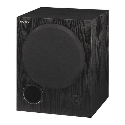
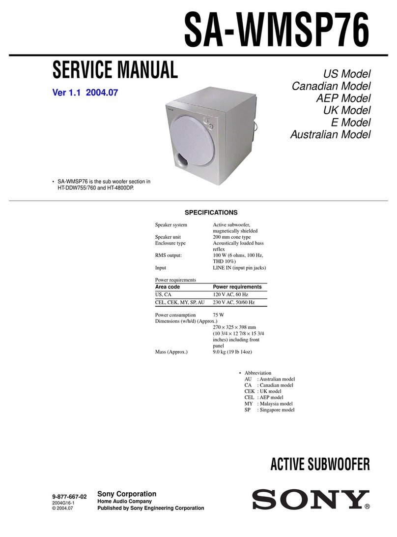
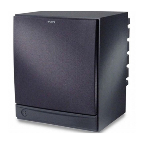
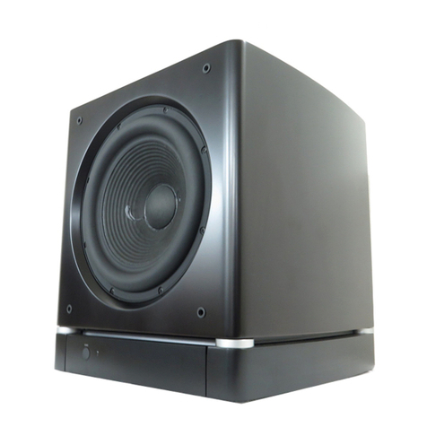
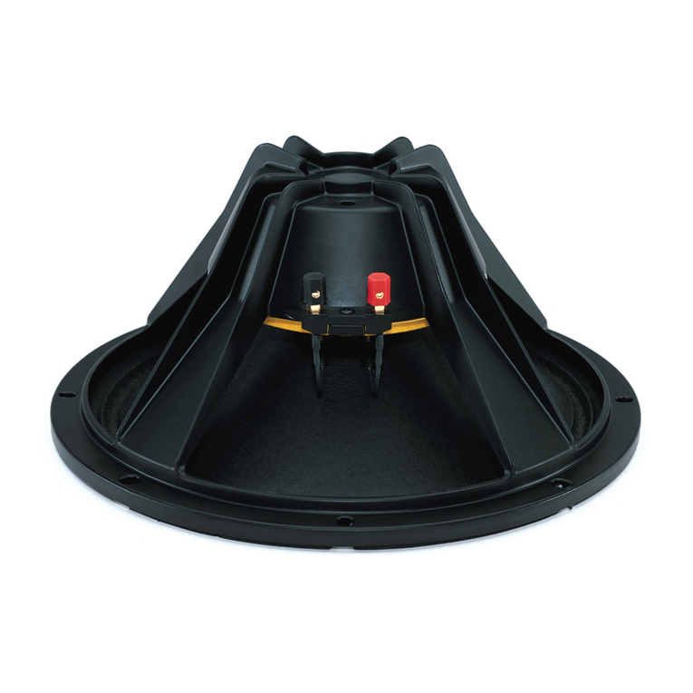
Sony SA-WX9000F User manual

SERVICE MANUAL
Sony Video & Sound Products Inc.
SA-WX9000F/WXF9000
ACTIVE SUBWOOFER
9-896-484-01
2018A33-1
© 2018.01
US Model
Canadian Model
SA-WX9000F
AEP Model
UK Model
SA-WXF9000
Ver. 1.0 2018.01
• SA-WX9000F is the active subwoofer in HT-X9000F.
• SA-WXF9000 is the active subwoofer in HT-XF9000.
• AlloftheunitsincludedintheHT-X9000F(SA-X9000F/SA-
WX9000F/Remote control) or HT-XF9000 (SA-XF9000/
SA-WXF9000/Remote control) are required to confirm-
ing operation of SA-WX9000F/WXF9000. Check in ad-
vance that you have all of the units.
• For the TEST MODE for this unit, refer to the service manual of HT-X9000F/XF9000.
SPECIFICATIONS
POWER OUTPUT (reference)
100 W (at 4 ohms, 100 Hz)
Speaker system
Subwoofer speaker system, Bass
reex
Speaker
160 mm (6 3/8 in.) cone type
Power requirements
120 V AC, 60 Hz (WX9000F: US, CND)
Power consumption
On: 20 W
Standby mode: 0.5 W or less
Dimensions (approx.) (w/h/d)
190 mm × 382 mm × 387 mm (7 1/2 in ×
15 1/8 in × 15 1/4 in) (not including
projection portion)
Mass (approx.)
7.8 kg (17 13/64 lb)
Frequency band
2.4 GHz (2.4000 GHz - 2.4835 GHz)
Modulation method
FHSS (Freq Hopping Spread Spectrum)
Design and specications are subject to
change without notice.
Wireless Receiver Section
220 V - 240 V AC, 50 Hz/60 Hz
(WXF9000: AEP, UK)
This system incorporates Dolby* Digital
and the DTS** Digital Surround System.
* Manufactured under license from Dolby
Laboratories. Dolby, Dolby Audio, Dolby
Atmos, Dolby Vision, and the double-D
symbol are trademarks of Dolby
Laboratories.
**For DTS patents, see http://
patents.dts.com. Manufactured under
license from DTS, Inc. DTS, the Symbol,
DTS and the Symbol together, DTS:X, and
the DTS:X logo are registered trademarks
and/or trademarks of DTS, Inc. in the
United States and/or other countries. ©
DTS, Inc. All Rights Reserved.
The BLUETOOTH®word mark and logos are
registered trademarks owned by Bluetooth
SIG, Inc. and any use of such marks by Sony
Corporation is under license. Other
trademarks and trade names are those of
their respective owners.
This system incorporates High-Denition
Multimedia Interface (HDMI™) technology.
The terms HDMI and HDMI High-Denition
Multimedia Interface, and the HDMI Logo
are trademarks or registered trademarks of
HDMI Licensing Administrator, Inc. in the
United States and other countries.
“BRAVIA” logo is a trademark of Sony
Corporation.
“ClearAudio+” is a trademark of Sony
Corporation.
WALKMAN® and WALKMAN® logo are
registered trademarks of Sony
Corporation.
“PlayStation” is a registered trademark or
trademark of Sony Interactive
Entertainment Inc.
MPEG Layer-3 audio coding technology
and patents licensed from Fraunhofer IIS
and Thomson.
Windows Media is either a registered
trademark or trademark of Microsoft
Corporation in the United States and/or
other countries.
This product is protected by certain
intellectual property rights of Microsoft
Corporation. Use or distribution of such
technology outside of this product is
prohibited without a license from Microsoft
or an authorized Microsoft subsidiary.
“DSEE” is a trademark of Sony Corporation.
“TRILUMINOS” and “TRILUMINOS” logo are
a registered trademark of Sony
Corporation.
All other trademarks are trademarks of
their respective owners.
Copyrights and Trademarks
SA-WX9000F/WXF9000
2
NOTES ON CHIP COMPONENT REPLACEMENT
• Never reuse a disconnected chip component.
• Notice that the minus side of a tantalum capacitor may be dam-
aged by heat.
SAFETY CHECK-OUT
After correcting the original service problem, perform the follow-
ing safety check before releasing the set to the customer:
Check the antenna terminals, metal trim, “metallized” knobs,
screws, and all other exposed metal parts for AC leakage.
Check leakage as described below.
LEAKAGE TEST
The AC leakage from any exposed metal part to earth ground and
from all exposed metal parts to any exposed metal part having a
return to chassis, must not exceed 0.5 mA (500 microamperes.).
Leakage current can be measured by any one of three methods.
1. A commercial leakage tester, such as the Simpson 229 or RCA
WT-540A. Follow the manufacturers’ instructions to use these
instruments.
2. A battery-operated AC milliammeter. The Data Precision 245
digital multimeter is suitable for this job.
3. Measuring the voltage drop across a resistor by means of a
VOM or battery-operated AC voltmeter. The “limit” indication
is 0.75 V, so analog meters must have an accurate low-voltage
scale. The Simpson 250 and Sanwa SH-63Trd are examples
of a passive VOM that is suitable. Nearly all battery operated
digital multimeters that have a 2 V AC range are suitable. (See
Fig. A)
1.5 kΩ0.15 μF
AC
voltmeter
(0.75 V)
To Exposed Metal
Parts on Set
Earth Ground
Fig. A. Using an AC voltmeter to check AC leakage.
SAFETY-RELATED COMPONENT WARNING!
COMPONENTS IDENTIFIED BY MARK 0OR DOTTED LINE
WITH MARK 0ON THE SCHEMATIC DIAGRAMS AND IN
THE PARTS LIST ARE CRITICAL TO SAFE OPERATION.
REPLACE THESE COMPONENTS WITH SONY PARTS
WHOSE PART NUMBERS APPEAR AS SHOWN IN THIS
MANUAL OR IN SUPPLEMENTS PUBLISHED BY SONY.
ATTENTION AU COMPOSANT AYANT RAPPORT
À LA SÉCURITÉ!
LES COMPOSANTS IDENTIFIÉS PAR UNE MARQUE 0SUR
LES DIAGRAMMES SCHÉMATIQUES ET LA LISTE DES
PIÈCES SONT CRITIQUES POUR LA SÉCURITÉ DE FONC-
TIONNEMENT. NE REMPLACER CES COMPOSANTS QUE
PAR DES PIÈCES SONY DONT LES NUMÉROS SONT DON-
NÉS DANS CE MANUEL OU DANS LES SUPPLÉMENTS
PUBLIÉS PAR SONY.
1. SERVICING NOTES ............................................. 3
2. DISASSEMBLY
2-1. Disassembly Flow........................................................... 6
2-2. AMP Block ..................................................................... 7
2-3. SK1 SUB MAIN Board .................................................. 8
2-4. Power-supply Cord ......................................................... 9
2-5. POWER Board................................................................ 10
2-6. Bluetooth Module ........................................................... 10
2-7. SK1-SUB-KEY Board, Button (Power-CZ2)................. 11
2-8. SK1-SUB-JACK Board .................................................. 11
2-9. SUB LED Board, Front Panel Assy................................ 12
2-10. Loudspeaker (160 mm)................................................... 13
3. TROUBLESHOOTING .......................................... 14
4. DIAGRAMS
4-1. Printed Wiring Board - SK1 SUB MAIN Board - .......... 17
4-2. Schematic Diagram - SK1 SUB MAIN Board (1/2) - .... 18
4-3. Schematic Diagram - SK1 SUB MAIN Board (2/2) - .... 19
4-4. Printed Wiring Boards - PANEL Section - ..................... 20
4-5. Schematic Diagram - PANLE Section -.......................... 21
4-6. Printed Wiring Board - POWER Board -........................ 22
4-7. Schematic Diagram - POWER Board - .......................... 23
5. EXPLODED VIEWS
5-1. Speaker Section............................................................... 25
5-2. AMP Section................................................................... 26
6. ELECTRICAL PARTS LIST .............................. 27
TABLE OF CONTENTS

SA-WX9000F/WXF9000
3
SECTION 1
SERVICING NOTES
UNLEADED SOLDER
Boards requiring use of unleaded solder are printed with the lead-
free mark (LF) indicating the solder contains no lead.
(Caution: Some printed circuit boards may not come printed with
the lead free mark due to their particular size)
: LEAD FREE MARK
Unleaded solder has the following characteristics.
• Unleaded solder melts at a temperature about 40 °C higher
than ordinary solder.
Ordinary soldering irons can be used but the iron tip has to be
applied to the solder joint for a slightly longer time.
Soldering irons using a temperature regulator should be set to
about 350 °C.
Caution: The printed pattern (copper foil) may peel away if
the heated tip is applied for too long, so be careful!
• Strong viscosity
Unleaded solder is more viscous (sticky, less prone to flow)
than ordinary solder so use caution not to let solder bridges
occur such as on IC pins, etc.
• Usable with ordinary solder
It is best to use only unleaded solder but unleaded solder may
also be added to ordinary solder.
NOTE OF REPLACING THE FUSE
The fuse is or could be in the neutral. When a fuse is being re-
placed, the main plug shall be disconnected from the AC outlet to
prevent electric shock.
ADVANCE PREPARATION WHEN CONFIRMING OP-
ERATION
All of the units included in the HT-X9000F (SA-X9000F/SA-
WX9000F/Remote control) or HT-XF9000 (SA-XF9000/SA-
WXF9000/Remote control) are required to confirming operation
of SA-WX9000F/WXF9000. Check in advance that you have all
of the units.
DISCHARGE PROCESSING
Before checking the operation of the boards for the electric shock
prevention, perform the discharge processing by connecting the
resistor at both ends of the specified capacitor with referring to the
figure below.
Note: Be sure to discharge using a resistor of 800 or higher.
– POWER Board (Conductor Side) –
C923
C917
800 :/2 W
800 :/2 W
NOTE OF PERFORMING THE OPERATION CHECK IN
THE STATE THAT HEAT SINK IS REMOVED
When performing the operation check in the state that this unit is
disassembled, it is possible to perform the operation check in the
state that heat sink is removed. However, don’t perform the opera-
tion check in the long time, and perform the operation check in the
volume state as low as possible.
The SERVICING NOTES contains important information for servicing. Be sure to read this section before repairing the unit.
ABOUT THE PROTECTION
qIf the power indicator on the
subwoofer flashes in red, press Æ
(power) of the subwoofer to turn off
the power and check whether the
ventilation holes of the subwoofer is
blocked or not.
MODEL IDENTIFICATION
Distinguish by Part No. and Destination code of the model number
label on the rear side of the main unit.
– Rear view – WX9000F: US, CND
WXF9000: AEP, UK
MODEL NUMBER LABEL
Destination code
Part No.
Destination code
Part No.
Destination Part No. Destination
code
WX9000F: US, CND 4-725-828-0[] UC2
WXF9000: AEP 4-725-830-0[] CEL
WXF9000: UK 4-725-831-0[] CEK
DESTINATION ABBREVIATIONS
The following abbreviations for model destinations are used in this
service manual.
• Abbreviations
AEP : European area (Except for UK, Ireland), East European
area, CIS area (Moldova) and Middle East area (Israel,
Jordan) models
CND : Canadian and Latin American area (Puerto Rico) models
UK : European area (UK and Ireland) model

SA-WX9000F/WXF9000
4
WIRELESS CONNECTION (LINK) WORK OF BAR SPEAK-
ER AND SUBWOOFER
When the Bluetooth module of bar speaker or Bluetooth module of
subwoofer are replaced, the wireless connection (LINK) of the bar
speaker and subwoofer will be disconnected.
Before returning repaired products to the customer, follow the pro-
cedure below to LINK the bar speaker and subwoofer.
Note: If only the bar speaker or subwoofer is brought in for repair, wire-
less connection (LINK) is not possible. Refer to “What to do if only
bar speaker or subwoofer are brought in for repair”.
Replacing parts for repairing that required wireless con-
nection (LINK)
• Replacing the Bluetooth module of bar speaker
• Replacing the Bluetooth module of subwoofer
Wireless connection (LINK) method
When the repairing unit is not secure link:
After replacing the Bluetooth module of the bar speaker or replac-
ing the Bluetooth module of the subwoofer, when turn the power
on, it will automatically wireless connection.
When the repairing unit was secure link:
After replacing the Bluetooth module of the bar speaker or replac-
ing the Bluetooth module of the subwoofer, even if turn the power
on, if you do not automatically wireless connection, there is a pos-
sibility that the repairing unit was secure link.
In this case, perform the secure link according to “Secure link
method” below.
Also, press and hold the [LINK] button on the rear side of sub-
woofer to cancel the secure link, it can automatically wireless con-
nection.
Secure link method
Procedure:
1. Connect bar speaker with TV monitor.
2. Press the [1] button on the bar speaker to turn the power on.
3. Press the [1] button on the rear side of subwoofer to turn the
power on.
4. Press the [HOME] button on the remote commander.
5. From the display of home menu on the TV monitor, operate
and decision in the following order.
“Setup” →“Advanced settings” →“Speaker settings” →“Se-
cure Link”→“On”
6. Press the [LINK] button on the rear side of subwoofer.
Note: Perform the next step within 2 minutes after the power indicator is
flashed.
7. From the display of home menu on the TV monitor, select the
“Start” and decision.
8. The message “Finish” is displayed on the TV monitor, the
power indicator of the subwoofer is lit in orange and secure
link is completed.
What to do if only bar speaker or subwoofer are brought
in for repair
If only the bar speaker or subwoofer is brought in for repair situa-
tion, and the Bluetooth module is replaced, by customer must wire-
less connection (LINK) the bar speaker and subwoofer.
• If the customer was not performing the secure link
It will automatically wireless connection (LINK) with the bar
speaker and subwoofer when turn the power on.
• If the customer was performing the secure link
The customer must need perform the secure link setting again, or
customer must need to cancel the secure link of the bar speaker or
subwoofer at hand of the customer and perform a normal wireless
connection.
Secure link cancellation method of bar speaker
Procedure:
1. Connect bar speaker with TV monitor.
2. Press the [1] button to turn the power on.
3. Press the [HOME] button on the remote commander.
4. From the display of home menu on the TV monitor, operate
and decision in the following order.
“Setup” →“Advanced settings” →“Speaker settings” →“Se-
cure Link”
5. Since the “On/Off” switching of Secure Link is displayed, se-
lect the “Off” and decision.
Secure link cancellation method of subwoofer
Procedure:
1. Press the [1] button on the rear side of subwoofer to turn the
power on.
2. Press and hold the [LINK] button on the rear side of subwoof-
er.
Press and hold the [LINK] button.
3. When the secure link is canceled, the power indicator is flashes
in green.

SA-WX9000F/WXF9000
5
NOTE OF REPLACING THE ELECTRICAL PARTS ON
EACH BOARDS FOR REPAIRING
Among mounted electrical parts on each boards, only parts that
are described in the electrical parts list can be replaced for repair.
The parts that are not described in the electrical parts list cannot be
replaced with single for repairing.
SPREADING OF COMPOUND
When the IC8104 on the SK1 SUB MAIN board or the SK1 SUB
MAIN board is replaced, spread the compound to the touching
portion between the IC8104 and the heat sink.
– SK1 SUB MAIN Board (Side A) –
IC8104
compound

SA-WX9000F/WXF9000
6
SECTION 2
DISASSEMBLY
• This set can be disassembled in the order shown below.
2-1. DISASSEMBLY FLOW
SET
2-4. POWER-SUPPLY CORD
(Page 9)
2-5. POWER BOARD
(Page 10)
2-6. BLUETOOTH MODULE
(Page 10)
2-7. SK1-SUB-KEY BOARD, BUTTON (POWER-CZ2)
(Page 11)
2-8. SK1-SUB-JACK BOARD
(Page 11)
2-2. AMP BLOCK
(Page 7)
2-3. SK1 SUB MAIN BOARD
(Page 8)
2-10. LOUDSPEAKER (160 mm)
(Page 13)
2-9. SUB LED BOARD, FRONT PANEL ASSY
(Page 12)
JIG
When disassembling the unit, use the following
jig for speaker removal.
Part No. Description
J-2501-238-A JIG FOR SPEAKER REMOVAL

SA-WX9000F/WXF9000
7
Note: Follow the disassembly procedure in the numerical order given.
2-2. AMP BLOCK
bottom side
rear side
top side
– Rear view –
Note 1: When removing the AMP block, remove the eighteen tapping screws
as shown below. If you remove screws other than those specified in
the below, the internal parts may fall out and get damaged.
(Removing the six screws at the vmark screws is not necessary.)
1three
tapping
screws
(3.5 u16)
1three
tapping
screws
(3.5 u16)
1three tapping screws
(3.5 u16)
1three
tapping
screws
(3.5 u16)
1three tapping screws
(3.5 u16)
1three
tapping
screws
(3.5 u16)
top side
vv
vv
vv
3Remove two wires
from the clamp (N).
(See Fig. A)
2Open the AMP block
in the direction of the
arrow.
rib
rib
hole
hole
4SUB LED board cable
connector (CN8111)
5speaker connection cable
connector (CN8103)
6AMP block
Note 2: When installing the AMP block,
align the two ribs and two holes.
:ire VeWWiQJ
SK1 SUB MAIN board
speaker connection cable
SUB LED board cable
clamp (N)
)iJ $!

SA-WX9000F/WXF9000
8
2-3. SK1 SUB MAIN BOARD
:LUHVHWWLQJ
terminal side
3POWER board cable
connector (CN8102)
4SK1-SUB-JACK board
cable connector
(CN8107)
2Remove two cables
from the clamp (N).
rear side
top side
bottom side
AMP block
1FFC (26P)
(CN8101)
SK1 SUB MAIN board
POWER board cable
POWER board
heat sink
top side
boss
5screw
(BVTP3 u8)
6clamp (N)
boss
hole
hole
hole
hole
rib
rib
5screw
(BVTP3 u8)
5screw
(BVTP3 u8)
5screw
(BVTP3 u8)
6clamp (N)
7Remove the SK1 SUB MAIN board
block in the direction of the arrow.
8screw
(BVTP3 u8)
8screw
(BVTP3 u8)
9heat sink (main)
Note 2: When installing the heat sink (main),
align the two bosses and two holes.
0SK1 SUB MAIN board
Note 3: When installing the SK1 SUB MAIN board,
align the two ribs and two holes.
SK1-SUB-JACK board cable
Note 4: The two cables must not touch the heat sink.
clamp (N)
Note 1: When the SK1 SUB MAIN board is replaced, spread the com-
pound to the touching portion between the IC8104 and the
heat sink.

SA-WX9000F/WXF9000
9
2-4. POWER-SUPPLY CORD
3RZHUVXSSO\FRUGEORFNVHWWLQJ
3RZHUVXSSO\FRUGVHWWLQJ
1power-supply cord
connector (CN901)
5cord bushing
(FBS001)
4Unlock.
3Draw out the power-supply
cord block from the hole. 6power-supply cord
power-supply cord
,QVWDOODWLRQSRVLWLRQRIWKHFRUG
EXVKLQJ)%6
power-supply cord
cord bushing
(FBS001)
lock side
90
+5, -0 mm
to POWER board
lock side
cord bushing (FBS001)
Note: When installing the power-supply cord block,
check the lock side position of the cord bushing
(FBS001) and install correctly.
hole
rear side
top side
bottom side
cord bushing (FBS001)
2two
claws
top side
bottom side
–,QQHUYLHZ–
top side
claw side
–,QQHUYLHZ–
AMP block
bottom side
bottom side
POWER board
[blue]
[brown]
[black]
[white] POWER board
:;)86&1'
:;)$(38.
claw side
claw side
claw
side
power-supply
cord
power-supply
cord

SA-WX9000F/WXF9000
10
2-5. POWER BOARD
2Remove two cables
from the clamp (N).
rear side
top side
bottom side
AMP block
1power-supply cord
connector (CN901)
4two screws
(BVTP3 u8)
hole
3POWER board cable
connector (CN8102)
4two screws
(BVTP3 u8)
5
6POWER board
Note 1: When installing the POWER board,
align the two ribs and two holes.
hole
rib
rib
:LUHVHWWLQJ
SK1 SUB MAIN board
POWER board cable
POWER board
heat sink
top side
SK1-SUB-JACK board cable
Note 2: The two cables must not touch the heat sink.
clamp (N)
2-6. BLUETOOTH MODULE
hole
4boss
5hook
2screw
(BVTP3 u8)
terminal side
1Draw the FFC (26P)
out of the connector.
front side
rear side
top side
AMP block
3Lift up the bluetooth module
in the direction of the arrow.
6bluetooth module
Note 2: When installing the
bluetooth module,
align the boss and hole.
Note 1: When the bluetooth module is replaced, be sure to refer to
“WIRELESS CONNECTION (LINK) WORK OF BAR
SPEAKER AND SUBWOOFER” on page 4.

SA-WX9000F/WXF9000
11
2-7. SK1-SUB-KEY BOARD, BUTTON (POWER-CZ2)
front side
rear side
top side
AMP block
hole
1SK1-SUB-JACK board cable
connector (CN8601)
2two screws
(BVTP3 u8)
3Remove the SK1-SUB-KEY board
block in the direction of the arrow.
5SK1-SUB-KEY board
Note 1: When installing the SK1-SUB-KEY
board, align the two bosses and two
holes.
SK1-SUB-KEY board (side A)
hole 4two non woven fabrics (T0.3)
(See Fig. B)
6Remove the button block in
the direction of the arrow.
7two non woven
fabrics (T0.3)
(See Fig. C)
8button (power-CZ2)
Note 2: When installing the button (power-CZ2),
align the six bosses and six holes.
– Rear view –
two non woven fabrics (T0.3)
button (power-CZ2)
non woven fabric (T0.3)push switch
guide line
guide line
(center)
guide line
(center)
guide line
< Fig. C >
3DVWLQJSRVLWLRQRIWKHQRQZRYHQIDEULF7
< Fig. B >
three bosses
boss
boss
three
bosses
total six holes
SK1-SUB-KEY board (side A)
2-8. SK1-SUB-JACK BOARD
3screw
(BVTP3 u8)
hole
5SK1-SUB-JACK board block
Note 1: When installing the SK1-SUB-JACK
board block, align the two bosses and
two holes.
1SK1-SUB-KEY board cable
connector (CN8508)
2SK1 SUB MAIN board cable
connector (CN8504)
front side
rear side
top side
:LUHVHWWLQJ
AMP block
Installation direction for
the lug terminal.
–,QQHUYLHZ–
bracket
(jack)
boss
4wire with lug
hole boss
6two screws
(BVTP3 u8)
rib
8SK1-SUB-JACK board
Note 2: When installing the
SK1-SUB-JACK board,
align the two ribs and
two holes.
7bracket (jack)
hole
hole
rib

SA-WX9000F/WXF9000
12
2-9. SUB LED BOARD, FRONT PANEL ASSY
0 front panel assy
Note 2: When installing the front panel assy,
peel off the used bond and apply a new
bond, then install the front panel assy.
6Remove the front panel block
in the direction of the arrow.
7SK1 SUB MAIN
board cable
connector
(CN7000)
bottom side
1Insert a flat-head screwdriver into
the two slits on the bottom of the unit,
and open a gap between the front
panel block and speaker cabinet.
front side
top side
top side
right side
bottom side
3 While moving the jig in the direction
of the arrow, remove four bosses.
2Insert the jig into the space and slowly
remove the front panel block.
Note 1: When using a jig, please work
carefully so as not to damage
the front panel block and
speaker cabinet.
speaker cabinet
front panel block
total four bosses
soft cloth, etc.
8two screws
(BVTP3 u8)
front side
top side
bottom side
total four bosses
front side
left side
5 While moving the jig in the direction
of the arrow, remove four bosses.
4Insert the jig into the space and
slowly remove the front panel
block.
Note 1: When using a jig, please
work carefully so as not
to damage the front
panel block and
speaker cabinet.
two slits
front panel block
front panel block hole
hole
two
bosses
9SUB LED board
Note 3: When installing the SUB LED board,
align the two bosses and two holes.

SA-WX9000F/WXF9000
13
2-10. LOUDSPEAKER (160 mm)
1six screws
(BVTP4 u20)
4loudspeaker (160 mm)
2Lift up the loudspeaker block
in the direction of the arrow.
loudspeaker
(160 mm)
6SHDNHUFRQQHFWLRQFDEOHVHWWLQJ
,QVWDOODWLRQGLUHFWLRQIRUWKHORXGVSHDNHUPP
terminals position
[gray]
[black]
3 terminal (wide)
[gray]
3 terminal (narrow)
[black]
Note 1: When installing the loudspeaker (160 mm),
make the position of terminals as shown in
the figure below.
top side
bottom side
Note 2: When connecting the speaker connection cable
terminal to the loudspeaker (160 mm), take care
for the direction of the terminal and connect it.
loudspeaker (160 mm)
top side
rear side
bottom side
OK NG
OK NG
–)URQWYLHZ–
top side
soft cloth, etc.

SA-WX9000F/WXF9000
14
SECTION 3
TROUBLESHOOTING
1. ON/STANDBY indicator flashes in red (PROTECT)
ON/STANDBY indicator flashes in
red.
(PROTECT)
IC8104 on the SK1 SUB MAIN
board is burned out.
ON/STANDBY indicator remains
flashing in red, when removing the
subwoofer connection connector
(CN8103) on the SK1 SUB MAIN
board and turning the power on.
Yes
Yes
Yes
No No
No
Check the subwoofer cable.
Check and replace the subwoofer
(SP1).
No
Check the mounted state of area surrounding IC8104 on the
SK1 SUB MAIN board do not short-circuits or opens. If there is
no abnormality, IC8104 on the SK1 SUB MAIN board might
have been damaged. Replace the IC8104 on the SK1 SUB
MAIN board.
Yes
The voltage of the following is 12 V.
SK1 SUB MAIN board: IC8001 pin 4
Replace the IC8104 on the SK1
SUB MAIN board.
Yes
Replace the SK1 SUB MAIN board.
(IC8001 on the SK1 SUB MAIN board might
have been damaged)
Resistor (R8129, R8130) on the
SK1 SUB MAIN board conduct the
electricity.
Replace the SK1 SUB MAIN board.

SA-WX9000F/WXF9000
SA-WX9000F/WXF9000
1515
2. ON/STANDBY indicator does not light up (Power is not turned on)
ON/STANDBY indicator does not
light up.
(Power is not turned on)
The voltage of the following is about
28.5 V.
POWER board: CN902 pin 1
The voltage of the following is 3.3 V.
SK1 SUB MAIN board:
CN8101 pin 9
Yes
POWER board might have been
damaged. Replace the POWER
board.
Yes
Yes
Yes
Fuse (F901, F902) and fusible
resistor (R923) on the POWER
board conduct the electricity.
No
No Check the pattern of area surrounding connector (CN8101) on
the SK1 SUB MAIN board and UNSW3.3V line. If there is no
abnormality, replace the Bluetooth module.
The reset signal is inputted to pin 21
(AC_CUT) of connector (CN8101)
on the SK1 SUB MAIN board after
AC input.
Check the mounted state of area
surrounding IC8102 on the SK1
SUB MAIN board, and repair it.
Yes
No
No
Even if the fuse (F901, F902) on the
POWER board is replaced, it will be
damaged.
(Fusible resistor (R923) on the POWER
board is damaged, replace the POWER
board)
The voltage of the following is 3.3 V.
SK1 SUB MAIN board: IC8000 pin 1
Yes
No Check the mounted state of area surrounding IC8000 on the
SK1 SUB MAIN board do not short-circuits or opens. If there is
no abnormality, replace the SK1 SUB MAIN board.
Check the area surrounding connector (CN8101) on the SK1
SUB MAIN board. If there is no abnormality, the Bluetooth
module or SK1 SUB MAIN board are abnormality. Replace the
Bluetooth module or SK1 SUB MAIN board.
Yes
3. The sound is not outputted
The waveform of the following is normal.
SK1 SUB MAIN board:
IC8103 pin 11 (MCLK)
IC8103 pin 22 (LRCLK)
IC8103 pin 23 (SCLK)
IC8103 pin 27 (SDIN4)
Yes
The sound is outputted from the
connector (CN8103) on the SK1 SUB
MAIN board.
No
Check the area surrounding IC8103 and connector
(CN8101) on the SK1 SUB MAIN board.
Check the flexible flat cable (FFC1) (between Bluetooth
module and CN8101).
If there is no abnormality, replace the Bluetooth module
or flexible flat cable (FFC1).
Check the LC circuit of
amplifier output.
(L8102, L8103, C8136,
C8137 and C8139 on the
SK1 SUB MAIN board)
Yes
No
The sound is not outputted.
The waveform is outputted from the
IC8104 pin 35 (OUT_B), 39 (OUT_A), 40
(OUT_A) on the SK1 SUB MAIN board.
Yes
Yes
The waveform is outputted
from the IC8103 pin 48 (PWM
_M_4), pin 49 (PWM_P_4) on
the SK1 SUB MAIN board.
No The reset signal inputted to
pin 4 of IC8104 on the SK1
SUB MAIN board from pin 37
of IC8103 on the SK1 SUB
MAIN board.
No The voltage of the following is 3.3 V.
SK1 SUB MAIN board:
IC8103 pin 9, 14, 35, 50
Check the mounted state of coil (L8101) on
the SK1 SUB MAIN board, and then replace
the SK1 SUB MAIN board.
No
The waveform of the following is normal.
SK1 SUB MAIN board:
IC8103 pin 16 (RESET)
IC8103 pin 18 (PDN)
IC8103 pin 19 (MUTE)
IC8103 pin 20 (SDA)
IC8103 pin 21 (SCL)
Yes
No
Yes
Yes
Check the contact between connector
(CN8103) on the SK1 SUB MAIN board
and subwoofer cable.
Check the contact between subwoofer
(SP1) and subwoofer cable.
Yes
Check the mounted state of area surrounding
IC8103 on the SK1 SUB MAIN board do not
short-circuits or opens. If there is no
abnormality, IC8103 on the SK1 SUB MAIN
board might have been damaged. Replace
the IC8103 on the SK1 SUB MAIN board.
Check the mounted state of area surrounding
IC8104 on the SK1 SUB MAIN board do not
short-circuits or opens. If there is no
abnormality, IC8104 on the SK1 SUB MAIN
board might have been damaged. Replace
the IC8104 on the SK1 SUB MAIN board.
No
Check the area surrounding connector
(CN8101) on the SK1 SUB MAIN board.
Check the flexible flat cable (FFC1) (between
Bluetooth module and CN8101).
If there is no abnormality, replace the
Bluetooth module or flexible flat cable (FFC1).

SA-WX9000F/WXF9000
SA-WX9000F/WXF9000
1616
SECTION 4
DIAGRAMS
THIS NOTE IS COMMON FOR PRINTED WIRING BOARDS AND SCHEMATIC DIAGRAMS.
(In addition to this, the necessary note is printed in each block.)
For Printed Wiring Boards.
Note:
• X: Parts extracted from the component side.
• Y: Parts extracted from the conductor side.
• : Pattern from the side which enables seeing.
(The other layers’ patterns are not indicated.)
Caution:
Pattern face side:
(Conductor Side)
Parts face side:
(Component Side)
Parts on the pattern face side seen
from the pattern face are indicated.
Parts on the parts face side seen from
the parts face are indicated.
Caution:
Pattern face side:
(SIDE B)
Parts face side:
(SIDE A)
Parts on the pattern face side seen
from the pattern face are indicated.
Parts on the parts face side seen from
the parts face are indicated.
• Indication of transistor.
C
B
These are omitted.
E
Q
For Schematic Diagrams.
Note:
• All capacitors are in μF unless otherwise noted. (p: pF)
50 WV or less are not indicated except for electrolytics
and tantalums.
• All resistors are in Ωand 1/4 W or less unless otherwise
specified.
• 2: Nonflammable resistor.
• 5: Fusible resistor.
• C: Panel designation.
Note:
The components identi-
fied by mark 0or dotted
line with mark 0are criti-
cal for safety.
Replace only with part
number specified.
Note:
Les composants identifiés
par une marque 0sont
critiques pour la sécurité.
Ne les remplacer que par
une pièce portant le nu-
méro spécifié.
• A: B+ Line.
• Voltages and waveforms are dc with respect to ground
wireless connection to the bar speaker (SA-X9000F/
XF9000).
no mark
: POWER ON
*: Impossible to measure
• Voltages are taken with VOM (Input impedance 10 M).
Voltage variations may be noted due to normal production
tolerances.
• Waveforms are taken with a oscilloscope.
Voltage variations may be noted due to normal production
tolerances.
• Circled numbers refer to waveforms.
• Signal path.
F: AUDIO (ANALOG)
J: AUDIO (DIGITAL)
Note 1: When the complete SK1 SUB MAIN board is re-
placed, spread the compound to the touching portion
between the IC8104 and the heat sink.
Note 2: Among mounted electrical parts on each board, only
parts that are described in the electrical parts list can
be replaced for repairing.
The parts that are not described in the electrical parts
list cannot be replaced with single for repairing. Note 1: When the complete SK1 SUB MAIN board is re-
placed, spread the compound to the touching portion
between the IC8104 and the heat sink.
Note 2: Among mounted electrical parts on each board, only
parts that are described in the electrical parts list can
be replaced for repairing.
The parts that are not described in the electrical parts
list cannot be replaced with single for repairing.
• Circuit Boards Location
SUB LED board
Bluetooth module
(BT1)
SK1 SUB MAIN board
SK1-SUB-KEY board
SK1-SUB-JACK board
POWER board

SA-WX9000F/WXF9000
SA-WX9000F/WXF9000
1717
4-1. PRINTED WIRING BOARD - SK1 SUB MAIN Board - • : Uses unleaded solder.
• See page 16 for Circuit Boards Location.
R8020
R8022
31
23
14
8
14
7
1
64
13
5
8
4
1
1
4
115
101
2
26
1
25
51
R8238
R8253
R8254
R8255
R8256
R8257
R8258
R8261
R8265
28
1
29
56
R8266
JL8100
JL8101
JL8102
JL8103
JL8104
JL8105
JL8106 JL8107
JL8108
JL8111
JL8112
JL8113
CL8133
JL8114
JL8115
JL8116
JL8117
JL8118
JL8119
JL8120
CN8101
CN8102
CN8103
CN8107 C8101
C8102
C8103
C8104
CN8111
Q8102
C8106 C8108
C8109 C8107
C8110
C8111
C8112
C8113
C8114
C8115
C8119
FB8001
C8120
C8121
C8122
C8123
D8100
C8124
C8125
C8126
C8127
C8128
R8101
C8129
R8102
R8103
R8105
R8106
R8108
C8130
R8109 C8131
IC8102
C8132
IC8103
C8133
IC8104
C8134
IC8105
C8135
C8136
C8137
R8110
C8138
R8111
C8139
R8112
R8118
C8140
R8119
CL8196
CL8197
CL8198
L8000
L8001
L8002
C8147
C8148
R8121
R8122
R8123
R8124
R8125
R8126
R8127
R8128
R8129
R8130
R8133
R8134
R8135
R8136
R8137
44
23
1
22
R8138
R8139
C8164
C8165
R8140
R8141
C8171
C8176
C8177
C8178
C8179
R8154
C8180
R8158
C8181
JC8105
R8159
C8183
JC8107
C8185
JC8109
C8186
R8161
R8162
R8163 JC8110
R8164
R8165
R8166
R8167 R8168
R8169
C8193
C8194
R8170
R8171
R8172
R8173
R8174
R8175
R8176
R8183
JL8001
C8000
C8001
C8002 C8003
Q8000
C8004
Q8001
C8005
C8008
C8009 C8010
C8011
C8012
C8013
C8014
4
1
3
2
C8016
C8017
D8001
R8000
FB8101
R8001
FB8102
R8002
FB8103
R8003
R8004
R8005
R8006 IC8000
IC8001
R8009
IC8002
R8010
R8011
R8012
R8018
R8026
R8028
L8101
L8102
L8103
R8227
R8229 R8230
R8237
CL8101
CL8102
CL8103 CL8104
CL8105
CL8106
CL8107
CL8108
CL8109
CL8110
CL8111
CL8113
CL8114
CL8115
CL8118 CL8119
CL8120
CL8121
CL8122 CL8123
CL8124
CL8125
CL8128
CL8130
CL8131
CL8132
CL8135
CL8136
CL8137
CL8138
CL8139
CL8140
CL8141
CL8142
CL8143
CL8144
CL8146
CL8147
CL8148
CL8149
CL8150
CL8151
CL8152
CL8153
CL8158
CL8160
CL8167
CL8169
CL8170
CL8171
CL8172
CL8173 CL8174
CL8175
CL8176
CL8177
CL8178
CL8179
CL8180
CL8186
CL8187
CL8188
CL8189
CL8190
CL8191
CL8192
CL8193
CL8194
CL8195
CL8199
CL8001
CL8002
CL8003
CL8004
CL8006
CL8200
CL8201
CL8134
SK1 SUB MAIN BOARD (SIDE A)
SK1 SUB MAIN BOARD (SIDE B)
1-982-509-
11
(11)
1-982-509-
11
(11)
E
EKKA
A
>03P>02P
>01P
(CHASSIS) (CHASSIS)
(CHASSIS)
(CHASSIS)(CHASSIS)
(CHASSIS)
SP1
(SUBWOOFER)
SUB LED
BOARD
CN7000
SK1-SUB-JACK
BOARD
CN8504
POWER
BOARD
CN902
BT1
BLUETOOTH
MODULE
FFC1
A
B
C
D
E
F
G
H
1 2 3 4 5 6 7 8 9 10 11
Note 1: When the IC8104 on the SK1 SUB MAIN board is
replaced, spread the compound to the touching por-
tion between the IC8104 and the heat sink.
Note 2: When the Bluetooth module is replaced, be sure to refer
to “WIRELESS CONNECTION (LINK) WORK OF
BAR SPEAKER AND SUBWOOFER” on page 4.
(Page 20)
(Page 20) (Page 22)

SA-WX9000F/WXF9000
SA-WX9000F/WXF9000
1818
4-2. SCHEMATIC DIAGRAM - SK1 SUB MAIN Board (1/2) - • See page 20 for Waveforms. • See page 24 for IC Block Diagrams.
1
23
0 6.7
1.7
3.2
1.6
1.6
3.2
3.2
25.2
25.2
14.1
14.1
28.1
28.1
28.1
14.1
28.1
28.1
28.1
3.3
3.4
3.3
0.6
1
1.8
3.2
0.2
1.6
0.9
3.2
3.2
3.2
3.3
3.2
2.7
2.8
1.6
1.6
0
1.8
11.9
11.9
1.1
3.2
1.6
1.6
2.3
3.3
7.7
3.2
3.2
11.9
2.4
2.4
1.6
2.4
4.9
3.3
1.7
1.6
3P
CN8111
LED(R) 1
LED(G) 2
VCC 3
26P
CN8101
1D_GND
2TAS_SD
3PCONT
4LED1
5LED0
6TAS_RESET_N
7SCL
8SDA
9BAT_P
10I2S_SCLK
11D_GND
12I2S_MCLK
13D_GND
14I2S_SDO
15D_GND
16I2S_LRCLK
17TAS_XPDN
18PVDD_STBY
19WIRED_ON
20UART_TX
21AC_CUT
22UART_RX
23WIRED_DET
24KEY_PAIR
25BT_BOOT
26D_GND
FB8102
FB8101
FB8103
JL8120
JL8119
JL8116
JL8117
100R8165
R8172 100
R8171 100
R8170 100
10k
R8112
R8102
0
R8101
0
10k
R8108
R8158 100
R8159 100
R8161
100
R8162 100
R8163 100
R8164 100
R8166 100
R8167 100
R8168 100
R8169 100
R8237 0
R8127
0
R8128
0
15P
CN8107
KEY_POWER 1
KEY_PAIR 2
D_GND 3
SDA 4
BT_BOOT 5
D_GND 6
UART_TX 7
PCONT 8
UART_RX 9
D_GND 10
3.3V 11
AGND 12
ANALOG SW 13
14WIRED_DET
15WIRED_ON
JL8113
JL8114
CL8101
CL8115
CL8102
CL8113
CL8160
CL8195
CL8194
CL8103
CL8167
CL8105
CL8118
CL8104
CL8121
CL8124
CL8110
CL8114
CL8109
CL8122
CL8108
CL8107
CL8106
CL8120
CL8119
CL8123
CL 8111
CL8133
0.1
C8164
CL8131
CL8141
CL8140
CL8188
CL8190
CL8189
CL8191
CL8186
CL8187
CL8138
CL8137
CL8136
CL8135
CL8192
CL8158
4.7k
R8176
4.7k
R8175
10k
R8174
10k
R8173
CL8125
R8183
10k
R8227
10k
16V
100
C8171
470
R8229
0
R8258
0
R8261
0
R8230
R8106 100
R8105 100
R8103 100
CL8196
CL8198
CL8197 CL8199
CL8200
CL8201
R8266
0
CL8132
CL8130
CL8128
0.1
C8165
CL8134
0.01
C8194
JL8115
0.047
C8131
CL8144
DA2J10100L
D8100
3.3k
R8126
PCONT
0.47
C8136
470
R8118
100
R8256
CL8148
TAS5534DGGR-S
IC8103
PWM_HPM_L
1
PWM_HPP_L
2
PWM_HPM_R
3
PWM_HPP_R
4
AVSS
5
PLL_FLTM
6
PLL_FLTP
7
VR_ANA
8
AVD D
9
ASEL_EMO2
10
MCLK
11
OSC_RES
12
DVSS2_CORE
13
DVDD2_CORE
14
EMO1
15
RESET
16
HP_SEL
17
PDN
18
MUTE
19
SDA
20
SCL
21
LRCLK
22
SCLK
23
SDIN1
24
SDIN2
25
SDIN3
26
SDIN4
27
VR_DIG
28
SDOUT
29
SCLKO
30
LRCLKO
31
TEST
32
PSVC
33
BKND_ERR
34
DVDD1_CORE
35
DVSS1_CORE
36
VAL ID
37
PWM_M_1
38
PWM_P_1
39
PWM_M_2
40
PWM_P_2
41
PWM_M_3
42
PWM_P_3
43
NC_44
44
NC_45
45
NC_46
46
NC_47
47
PWM_M_4
48
PWM_P_4
49
AVDD_PWM
50
AVSS_PWM
51
VR_PWM
52
NC_53
53
NC_54
54
NC_55
55
NC_56
56
0R8265
10
C8115
CL8193
CL8178
0.1
C8178
10
C8126
JL8104 CL8142
CL8175
D_GND
0
R8130
15kR8121
47k
R8110
47
R8255
TAS5614LA-S
IC8104
GVDD_AB
1
VDD
2
OC_ADJ
3
RESET
4
INPUT_A
5
INPUT_B
6
C_START
7
DVDD
8
GND_9
9
GND_10
10
GND_11
11
GND_12
12
AVD D
13
INPUT_C
14
INPUT_D
15
FAULT
16
OTW
17
CLIP
18
M1
19
M2
20
M3
21
GVDD_CD
22
BST_D
23
BST_C
24
GND_25
25
GND_26
26
OUT_D_27
27
OUT_D_28
28
PVDD_CD_29
29
PVDD_CD_30
30
PVDD_CD_31
31
OUT_C
32
GND_33
33
GND_34
34
OUT_B
35
PVDD_AB_36
36
PVDD_AB_37
37
PVDD_AB_38
38
OUT_A_39
39
OUT_A_40
40
GND_41
41
GND_42
42
BST_B
43
BST_A
44
100R8111
CL8139
10k
R8154
10
C8177
JL8102
0.01
C8127
JL8107
CL8143
CL8174
10P
CN8102
1 D28.5V
2 PVDD_SEL
3
HI-TEMP/VACS_REQ
4DGND
5PVDD
6PVDD
7PVDD
8PGND
9PGND
10 PGND
0.01
C8193
18kR8122
47
R8254
PST8429UL
IC8102
GND
1
VDD
2
CD
3
OUT
4
0.047
C8114
CL8146
10k
R8123
CL8151
0.1
C8176
JL8105
1C8124JL8100
CL8172
CL8173
UNSW3.3V
1
C8132
470
R8125
PCM1808PWR
IC8105
1
Vref
2
AGND
3
AVc c
4
DVdd
5
DGND
6
SCKI
7
LRCK
8
BCK
9
DOUT
10
MOD0
11
MOD1
12
FMT
13
VinL
14
VinR
47
R8135
0.0047
C8108
JL8118
1
C8119
CL8149
47p
C8183
JL8103
1
C8129
JL8101
CL8171
10
R8141
0.01
C8102
12V
35V
470
C8140
47
R8136
0.047
C8113
0.01
C8147
1
C8120
JL8112
22
C8185
2.2
R8137
JL8106
CL8170
10
R8140
0.022
C8104
LSCR523UBFS8TL
Q8102
A_GND
0
R8129
10k
R8134
10
C8107
CL8150
4P
CN8103
SW+1
SW+2
SW–3
SW–4
10k
R8238
CL8153
22
C8186
30kR8139
10
C8181
JL8108
10
C8128
0.01
C8112
470p
C8134
35V
470
C8138
A5V
47
R8133
100k
R8109
0.0047
C8106
CL8147
6.3V
100
C8110
0.01
C8148
CL8176
0.1
C8180
2.2
R8138
0.33
C8101
1
C8133
1000p
C8137
PVDD
10
C8122
10
C8109
CL8152
0.01
C8103
CL8180
CL8177
0
R8257
1C8125
470p
C8135
0.047
C8130
1000p
C8139
D3.3V
10k
R8124
PVDD_GND
0.1
C8121
470
R8119
47
R8253
JL8111
LED_UNSW3.3V
6.3V
C8 111
470
CL8169
CL8179
10
C8179
0.1C8123
10uH
L8103
10uH
L8102
10uH
L8101
JC8107
0
JC8110
0
JC8109
0
JC8105
0
SUB_28.5V
CN8504
BOARD
SK1-SUB-JACK
>02S
SK1 SUB MAIN BOARD (1/2)
SUB LED
BOARD
>01S
CN7000
BLUETOOTH
MODULE
BT1
FFC1
CN902
A/D CONVERTER
>03S
DIGITAL POWER AMP
IC8105
BOARD
IC8104
RESET SIGNAL GENERATOR
>001S
BOARD
STREAM PROCESSOR
IC8102
SK1 SUB MAIN
POWER
IC8103
(2/2)
SP1
(SUBWOOFER)
RESET SWITCH
(CHASSIS)
(CHASSIS)
(CHASSIS)
(CHASSIS)
(CHASSIS)
(CHASSIS)
10 11 12 13 14 15
G
16
H
17
I
18
F
20 211
C
J
D
6
E
K
2
B
3
A
45 7 1989
Note 1: When the IC8104 on the SK1 SUB MAIN board is
replaced, spread the compound to the touching por-
tion between the IC8104 and the heat sink.
Note 2: When the Bluetooth module is replaced, be sure
to refer to “WIRELESS CONNECTION (LINK)
WORK OF BAR SPEAKER AND SUBWOOFER”
on page 4.
(Page 19)
(Page 23)
(Page 21)
(Page 21)

SA-WX9000F/WXF9000
SA-WX9000F/WXF9000
1919
4-3. SCHEMATIC DIAGRAM - SK1 SUB MAIN Board (2/2) -
1
11.9
28.1
3.3
3.3
4.9
5.8
3.3
7.7
5
3.3
0
28.1
0.8
0.9
0.8
3.3
3.3
0
4
1
C8008
6.3V
C8011
470
SUB_28.5V
PVDD_GND
D_GND
PVDD
PCONT
A_GND
D3.3V
UNSW3.3V
12V
A5V
JL8001
100k
R8018
10k
R8020
10k
R8022
0
R8026
MM3411A50URE
IC8002
CE
1
GND
2
VOUT
3
VDD
4
SI-3010KM-TLA
IC8001
VC
1
VIN
2
GND
3
VOUT
4
ADJ
5
RT7272BGSP
IC8000
SW
1
BOOT
2
EN
3
GND
4
FB
5
COMP
6
RLIM
7
VIN
8
LED_UNSW3.3V
0
R8028
50V
47
C8009
16V
100
C8010
0.1
C8012
0.1
C8013
1
C8014
1
C8016
4.7
C8017
10
C8000
10
C8004
0.0022
C8001 15k
R8009
1k
R8002
2.2k
R8006 4.7k
R8003
1.5k
R8004
0
R8001
10k
R8005
100k
R8000
0.1
C8005
CL8001
CL8003
CL8006
CL8002
R8011
0
33k
R8010
S
NTJS3151PT1G
Q8001
1
2
3
4
5
6
LTC014EUBFS8TL
Q8000
10k
R8012
22
C8002
22
C8003
FB8001
CL8004
DZ2J062M0L
D8001
2.2uH
L8001
4.7uH
L8000
2.2uH
L8002
>001S
SK1 SUB MAIN
BOARD
(1/2)
+5V REGULATOR
IC8002
+12V REGULATOR
IC8001
(2/2)SK1 SUB MAIN BOARD
DC/DC CONVERTER
IC8000
B+ SWITCH
Q8000, 8001
F
1
C
D
6
E
2
B
3
A
45 78 9
(Page 18)
• See page 20 for Waveforms. • See page 24 for IC Block Diagrams.

SA-WX9000F/WXF9000
SA-WX9000F/WXF9000
2020
• Waveforms
– SK1 SUB MAIN Board –
83.5 ns
3.4 Vp-p
1IC8103 qa (MCLK)
1 V/DIV, 50 ns/DIV
20.8 Ps
3.5 Vp-p
2IC8103 ws (LRCLK)
1 V/DIV, 10 Ps/DIV
3IC8103 wd (SCLK)
1 V/DIV, 200 ns/DIV
320 ns
3.5 Vp-p
4IC8000 2(BOOT)
10 V/DIV, 2 Ps/DIV
3.2 Ps
33.2 Vp-p
4-4. PRINTED WIRING BOARDS - PANEL Section - • : Uses unleaded solder.
• See page 16 for Circuit Boards Location.
13
S8601S8602
CN8601
C8601
C8602
CL8601
CL8602
CL8603
17
115
13 CL8501
CL8502
CN8504
CN8506
CN8508
C8501
C8508
R8501
R8502
JL8503
JL8504
JL8505
JL8506
JL8507
JL8508
JL8509
JL8510
JL8511
JL8512
JL8513
J8501
D7002
3
1
CL7000
CL7001
CL7002
CN7000
R7000
R7002
D7001
SK1-SUB-KEY BOARD (SIDE A)
SK1-SUB-KEY BOARD (SIDE B)
1-982-591-
11
(11)
1-982-591-
11
(11)
S8601, 8602
SK1-SUB-JACK BOARD (SIDE A)
1-982-552-
11
(11)
1-982-552-
11
(11)
SK1-SUB-JACK BOARD (SIDE B)
>02P
SUB LED BOARD (SIDE A)
SUB LED BOARD (SIDE B)
1-894-327-
11
(11)
1-894-327-
11
(11)
D7001, 7002
AK
AK
AK
(ON INDICATOR)
(STANDBY INDICATOR)
SK1 SUB MAIN
BOARD
CN8111
>01P
LINK
(NC)
SUBWOOFER
WIRED CONNECTION
SK1 SUB MAIN
BOARD
CN8107
(BRACKET) (BRACKET)
A
B
C
D
E
F
1 2 3 4 5 6
(Page 17)
(Page 17)
This manual suits for next models
1
Table of contents
Other Sony Subwoofer manuals

Sony
Sony SA-WX90 User manual

Sony
Sony SA-W90 User manual

Sony
Sony XS-L10S Manual

Sony
Sony SA-iP001P User manual

Sony
Sony XS-L120B5D User manual

Sony
Sony XS-AW81P5 User manual

Sony
Sony SA-W10 User manual

Sony
Sony SAW-M20 User manual

Sony
Sony XS-L1046 - 10" Component Woofer User manual

Sony
Sony SS-WG99 User manual

Sony
Sony XS-L100P5H Marketing User manual

Sony
Sony SA-WCT260H User manual

Sony
Sony SA-WMSP2 User manual

Sony
Sony XS-L101P5W Product guide

Sony
Sony SA-WD200 User manual

Sony
Sony XS-L1246 - 12" 400 Watt Subwoofer Product guide

Sony
Sony SA-CS9 User manual

Sony
Sony SA-WM500 User manual

Sony
Sony SA-WX900 User manual

Sony
Sony SA-W301 User manual