Spansion MB39C502-EVBSK-01 User manual

The following document contains information on Cypress products.

MB39C502-EVBSK-01
High Efficiency
Single Output Step Down DC/DC Controller
Evaluation Board
Operation Manual
Publication Number MB39C502-EVBSK-01_SS901-00030 Revision 1.0 Issue Date November 19, 2014
CONFIDENTIAL ver1.1

O p e r a t i o n M a n u a l
2 MB39C502-EVBSK-01_SS901-00030-1v0-E, November 19, 2014
CONFIDENTIAL ver1.1

O p e r a t i o n M a n u a l
November 19, 2014, MB39C502-EVBSK-01_SS901-00030-1v0-E 3
CONFIDENTIAL ver1.1
Preface
This manual explains how to use the evaluation board. Be sure to read this manual before using the product.
For this product, consult with sales representatives or support representatives.
Handling and use
Handling and use of this product and notes regarding its safe use are described in the manuals.
Follow the instructions in the manuals to use this product.
Keep this manual at hand so that you can refer to it anytime during use of this product.
Notice on this document
All information included in this document is current as of the date it is issued. Such information is subject to
change without any prior notice.
Please confirm the latest relevant information with the sales representatives.

O p e r a t i o n M a n u a l
4 MB39C502-EVBSK-01_SS901-00030-1v0-E, November 19, 2014
CONFIDENTIAL ver1.1
Caution of the products described in this document
The following precautions apply to the product described in this manual.
WARNING
Indicates a potentially hazardous situation which could result in death or serious injury and/or
a fault in the user’s system if the product is not used correctly.
Electric shock,
Damage
Before performing any operation described in this manual, turn off all the power supplies to the
system.
Performing such an operation with the power on may cause an electric shock or device fault.
Electric shock,
Damage
Once the product has been turned on, do not touch any metal part of it.
Doing so may cause an electric shock or device fault.
CAUTION
Indicates the presence of a hazard that may cause a minor or moderate injury, damages to
this product or devices connected to it, or may cause to loose software resources and other
properties such as data, if the device is not used appropriately.
Cuts, Damage
Before moving the product, be sure to turn off all the power supplies and unplug the cables.
Watch your step when carrying the product. Do not use the product in an unstable location
such as a place exposed to strong vibration or a sloping surface. Doing so may cause the
product to fall, resulting in an injury or fault.
Cuts
The product contains sharp edges that are left unavoidably exposed, such as jumper plugs.
Handle the product with due care not to get injured with such pointed parts.
Damage
Do not place anything on the product or expose the product to physical shocks. Do not carry
the product after the power has been turned on.
Doing so may cause a malfunction due to overloading or shock.
Damage
Since the product contains many electronic components, keep it away from direct sunlight,
high temperature, and high humidity to prevent condensation. Do not use or store the product
where it is exposed to much dust or a strong magnetic or electric field for an extended period
of time. Inappropriate operating or storage environments may cause a fault.
Damage
Use the product within the ranges given in the specifications.
Operation over the specified ranges may cause a fault.
Damage
To prevent electrostatic breakdown, do not let your finger or other object come into contact
with the metal parts of any of the connectors. Before handling the product, touch a metal
object (such as a door knob) to discharge any static electricity from your body.
Damage
When turning the power on or off, follow the relevant procedure as described in this document.
Before turning the power on, in particular, be sure to finish making all the required
connections. Furthermore, be sure to configure and use the product by following the
instructions given in this document. Using the product incorrectly or inappropriately may cause
a fault.
Damage
Always turn the power off before connecting or disconnecting any cables from the product.
When unplugging a cable, unplug the cable by holding the connector part without pulling on
the cable itself. Pulling the cable itself or bending it may expose or disconnect the cable core,
resulting in a fault.
Damage
Because the product has no casing, it is recommended that it be stored in the original
packaging. Transporting the product may cause a damage or fault. Therefore, keep the
packaging materials and use them when re-shipping the product.

O p e r a t i o n M a n u a l
November 19, 2014, MB39C502-EVBSK-01_SS901-00030-1v0-E 5
CONFIDENTIAL ver1.1
Table of Contents
1. Description ..................................................................................................................................... 8
2. Evaluation Board Specification....................................................................................................... 9
3. Pin Description ............................................................................................................................. 10
4. Setup and Checkup...................................................................................................................... 11
5. Component Layout....................................................................................................................... 12
6. Wiring Layout ............................................................................................................................... 13
7. Circuit Diagram............................................................................................................................. 14
8. Parts List ...................................................................................................................................... 15
9. Reference Data ............................................................................................................................ 16
10. Initial Settings............................................................................................................................... 22
11. Evaluation board picture............................................................................................................... 23
12. Ordering Information..................................................................................................................... 24
13. Major Changes............................................................................................................................. 25

O p e r a t i o n M a n u a l
6 MB39C502-EVBSK-01_SS901-00030-1v0-E, November 19, 2014
CONFIDENTIAL ver1.1
Figures
Figure 4-1 Image of Connection.............................................................................................................11
Figure 5-1 Component Layout............................................................................................................... 12
Figure 6-1 Wiring Layout ....................................................................................................................... 13
Figure 7-1 Circuit Diagram..................................................................................................................... 14
Figure 9-1 Efficiency vs Output Current, VOUT ; 1.2V-Setting............................................................... 16
Figure 9-2 Load regulation Output Voltage vs Output Current, VOT ; 1.2V-Setting............................... 16
Figure 9-3 Start-up (EN=0V=>5V) VIN=7.4V,VOUT=1.2V,IOUT=0.05A, SLP_N=H.............................. 17
Figure 9-4 Shutdown (EN=5V=>0V) VIN=7.4V,VOUT=1.2V,IOUT=0.05A, SLP_N=H........................... 17
Figure 9-5 Load step response (VIN=7.4V,VOUT=1.2V) IOUT=0.05A to 7.69A, SLP_N=H.................. 18
Figure 9-6 Load step response (VIN=7.4V,VOUT=1.2V) IOUT=7.69A to 0.05A, SLP_N=H.................. 18
Figure 9-7 Switching waveform (VIN=7.4V,Iout=8.54A) , SLP_N=H...................................................... 19
Figure 9-8 Switching waveform (VIN=7.4V,Iout=0.05A), SLP_N=H....................................................... 19
Figure 9-9 Switching waveform (VIN=7.4V,Iout=0.3A), LPM at SLP_N=L............................................. 20
Figure 9-10 Switching waveform (VIN=7.4V,Iout=0.01A) , LPM at SLP_N=L........................................ 20
Figure 9-11 Increase Temperature 1.2V Output Voltage, using “FDMC7208S” FET. ............................. 21
Figure 11-1 Evaluation board Picture (top) ............................................................................................ 23
Figure 11-2 Evaluation board Picture (back).......................................................................................... 23

O p e r a t i o n M a n u a l
November 19, 2014, MB39C502-EVBSK-01_SS901-00030-1v0-E 7
CONFIDENTIAL ver1.1
Tables
Table 2-1 Evaluation Board Specification ................................................................................................ 9
Table 3-1 Pin Description....................................................................................................................... 10
Table 8-1 Parts List................................................................................................................................ 15
Table 12-1 Ordering Information............................................................................................................ 24
Table 13-1 Major Changes..................................................................................................................... 25

8 MB39C502-EVBSK-01_SS901-00030-1v0-E, November 19, 2014
CONFIDENTIAL ver1.1
MB39C502-EVBSK-01
High Efficiency
Single Output Step Down DC/DC Controller
Evaluation Board
Operation Manual
1. Description
MB39C502 is a single output step down DC/DC controller using external FETs. It achieves the high
efficiency with “Enhanced Low Power Mode (LPM) Operation” in light load. In Enhanced LPM, this controller
operates that the quiescent current is reduced only 30μA and the switching frequency is fallen by extending
on time. These operations enable to improve the efficiency in light load. Internal compensation circuit with
current mode architecture and internal boost switch allow reducing the BOM parts and the component area.
“Over Current Alerting function” can detect the near over current limitation. The over current alerting level is
set 85% for over current limitation level. The function suppresses an excessive margin design through
elimination of possibilities of current overflows and enhances the system reliability.

O p e r a t i o n M a n u a l
November 19, 2014, MB39C502-EVBSK-01_SS901-00030-1v0-E 9
CONFIDENTIAL ver1.1
2. Evaluation Board Specification
Table 2-1 Evaluation Board Specification
Component
Symbol
Condition
Min
Typ
Max
Unit
Input Voltage
VIN
-
4.0
-
25
V
Output Voltage
VOUT
-
-
1.2
-
V
Output Current
IOUT
SLP_N=H
-
-
8.54
A
Switching Frequency
fSW
-
-
800
-
kHz

O p e r a t i o n M a n u a l
10 MB39C502-EVBSK-01_SS901-00030-1v0-E, November 19, 2014
CONFIDENTIAL ver1.1
3. Pin Description
Table 3-1 Pin Description
Component
Input or Output
Description
VIN
Input
Power supply terminal of DC/DC system.
VOUT
Output
Output of DC/DC system.
VDD
Input
Power supply terminal PWM controller and internal drivers.
EN
Input
Enable input for PWM Controller.
When turning on, apply greater than 0.65V and less than 5.5V.
When turning off, apply less than 0.25V.
SLP_N
Input
Input terminal transferred to “Enhanced LPM”.
Transferred to “Enhanced LPM”by connecting to “L”level.
PWRGD
Output
Open drain output terminal with power good.
ALERT_N_VOUT
Output
Open drain output terminal with over current alerting.
PGND
-
Power Ground Terminal.

O p e r a t i o n M a n u a l
November 19, 2014, MB39C502-EVBSK-01_SS901-00030-1v0-E 11
CONFIDENTIAL ver1.1
4. Setup and Checkup
−Supply the DC/DC input power of to the terminal between VIN to PGND.
−Supply the PWM controller input voltage of 5.0V to VDD terminal.
−Connect the VOUT terminal to required loading device or measuring instrument. In this time, connect
the EN terminal to “L” state.
Then, turning on the EN input. Confirming the DC/DC output voltage is setting voltage.
Note:
−The recommended operating conditions of MB39C502 EN pin is 5.5V maximum. Please don’t
connect EN to VIN when VIN voltage is over 5.5V.
Figure 4-1 Image of Connection

O p e r a t i o n M a n u a l
12 MB39C502-EVBSK-01_SS901-00030-1v0-E, November 19, 2014
CONFIDENTIAL ver1.1
5. Component Layout
Figure 5-1 Component Layout
Top View
O p e r a t i o n M a n u a l
November 19, 2014, MB39C502-EVBSK-01_SS901-00030-1v0-E 13
CONFIDENTIAL ver1.1
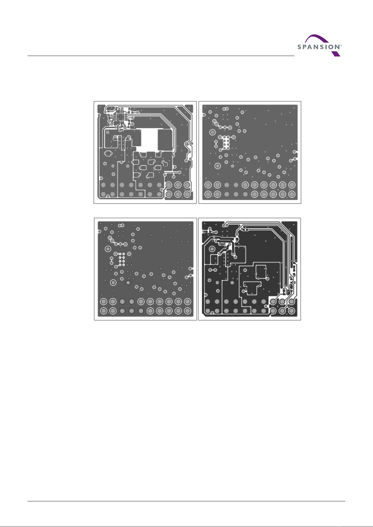
6. Wiring Layout
Figure 6-1 Wiring Layout
Top Side (Layer 1) Inside (Layer 2)
Inside (Layer 3) Bottom Side (Layer 4)

O p e r a t i o n M a n u a l
14 MB39C502-EVBSK-01_SS901-00030-1v0-E, November 19, 2014
CONFIDENTIAL ver1.1
7. Circuit Diagram
Figure 7-1 Circuit Diagram
VCC
FB
PWRGD
ALERT_N
VIN
VDD
BST
DRVH
CSP
CSN
SLP_N
EN
AGND
ILIM
PGND
DRVL
LX
11
8
9
3
7
2
15
13
16
6
4
5
1
17
10
14
12
M1
G
DS1
S2
S3
Q1
4
3
29
1
G
DS1
S2
S3
Q1
7
6
510
8
1L1
2
1D3
C1-1
C1-2
C1-3
VOUT
C2-2
2 1
R28
NMT
. .
C2-11
C8
C7
2
1
C5
2
1
C6
2
1
R4 21
LDO5
.. PatternShort
R18
EN 1
SLP_N 1
PWRGD
ALERT_N_VOUT
VIN
VIN
VDD
1
R2
2
R1-2
2
1
R21
21
R15
R14
VCC
VCC
R27
2
1
VINs
1
VOUTs 1
VIN
C2-1
2 1
PatternShort
VOUT1
PGND1
1PGNDs
VOUT2
VOUT3
PGND2
PGND3
VIN1
VIN2
VIN3
. .
R30
VCC
LX
C2-3
C2-4
C2-5
C2-6
C2-7
C2-8
C2-9
C2-10
VOUT4
PGND4
VIN4
VOUT5
PGND5
R29
VCC
1
2
R1-1
O p e r a t i o n M a n u a l
November 19, 2014, MB39C502-EVBSK-01_SS901-00030-1v0-E 15
CONFIDENTIAL ver1.1
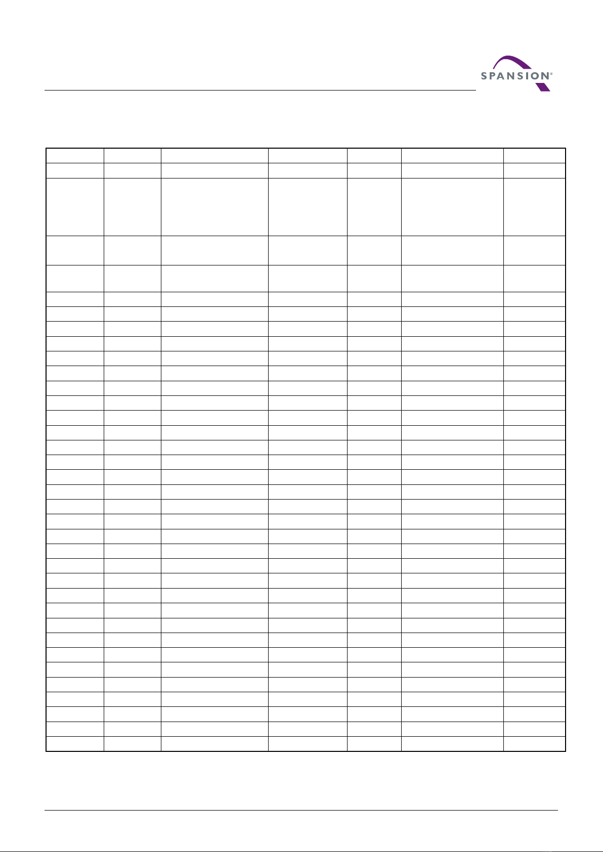
8. Parts List
Table 8-1 Parts List
Component
Item
Specification
Vender
Package
Parts Name
Remark
M1
IC
Spansion
QFN-16
MB39C502
Controller
Q1
Nch FET
VDS=30V, ID=11A
RON=8.8mΩ, QG=6.7nC
VDS=30V, ID=13.5A
RON=5.3mΩ, QG=14nC
Fairchild
Power33
FDMC7208S
High/Low
Side FET
D3
SBD
VF=0.35V at IF=10mA
On Semi-
conductor
1.6 x
0.8mm
BAT54XV2T1G
BST
L1
Inductor
1.0μH(10.6A)
ALPS
7.4 x
6.5mm
GLMC1R503A
LX
C1-1
Capacitor
10μF(35V)
TDK
2012
C2012X5R1V106K
VIN
C1-2
Capacitor
10μF(35V)
TDK
2012
C2012X5R1V106K
VIN
C1-3
Capacitor
1.0μF(50V)
TDK
1608
C1608X5R1H105K
VIN
C2-1 *
- *
- *
- *
- *
- *
No Mount *
C2-2 *
- *
- *
- *
- *
- *
No Mount *
C2-3
Capacitor
47μF(10V)
TDK
2012
C2012X5R1A476M
VOUT
C2-4
Capacitor
47μF(10V)
TDK
2012
C2012X5R1A476M
VOUT
C2-5
Capacitor
47μF(10V)
TDK
2012
C2012X5R1A476M
VOUT
C2-6
Capacitor
47μF(10V)
TDK
2012
C2012X5R1A476M
VOUT
C2-7
Capacitor
47μF(10V)
TDK
2012
C2012X5R1A476M
VOUT
C2-8
Capacitor
47μF(10V)
TDK
2012
C2012X5R1A476M
VOUT
C2-9
Capacitor
47μF(10V)
TDK
2012
C2012X5R1A476M
VOUT
C2-10
Capacitor
47μF(10V)
TDK
2012
C2012X5R1A476M
VOUT
C2-11
Capacitor
10μF(10V)
TDK
1608
C1608X5R1A106K
VOUT
C5
Capacitor
0.47μF(35V)
TDK
1005
C1005X5R1V474K
BST
C6
Capacitor
1.0μF(35V)
TDK
1005
C1005X5R1V105K
VIN
C7
Capacitor
1.0μF(35V)
TDK
1005
C1005X5R1V105K
VCC
C8
Capacitor
4.7μF(10V)
TDK
1005
C1005X5R1A475K
VDD
R1-1 *
Resistor *
0Ω(Jumper) *
KOA *
1005 *
RK73Z1E *
FB *
R1-2
Resistor
21.5kΩ
TE Connectivity
1005
CPF0402B21K5E1
FB
R2
Resistor
30.1kΩ
TE Connectivity
1005
CPF0402B30K1E1
FB
R4
Resistor
2mΩ
SSM
2012
KRL2012MR002F
RSENSE
R14 *
Resistor *
330kΩ *
KOA *
1005 *
RK73B1ETTP334J *
PWRGD *
R15 *
Resistor *
330kΩ *
KOA *
1005 *
RK73B1ETTP334J *
ALERT_N *
R18
-
-
-
-
-
No Mount
R21 *
- *
- *
- *
- *
- *
No Mount *
R27 *
Resistor *
220kΩ *
KOA *
1005 *
RK73B1ETTP224J *
EN *
R28 *
- *
- *
- *
- *
- *
No Mount *
R29 *
Resistor *
220kΩ *
KOA *
1005 *
RK73B1ETTP224J *
SLP_N *
R30
Resistor
10Ω
SSM
1005
RG1005PD100
VDD
-
Pin
3A
HIROSE
2.54
HIF3H-20PB-2.54DSA
-
*: parts on buck side

O p e r a t i o n M a n u a l
16 MB39C502-EVBSK-01_SS901-00030-1v0-E, November 19, 2014
CONFIDENTIAL ver1.1
9. Reference Data
Figure 9-1 Efficiency vs Output Current, VOUT ; 1.2V-Setting
Figure 9-2 Load regulation Output Voltage vs Output Current, VOT ; 1.2V-Setting
0%
10%
20%
30%
40%
50%
60%
70%
80%
90%
100%
0.0001 0.001 0.01 0.1 1 10
Efficiency
Output Current / A
Efficiency vs Output Current, VOUT ;1.2V-Setting
7.4V Normal 12.0V Normal 20.0V Normal
7.4V LPM 12.0V LPM 20.0V LPM
1.188
1.192
1.196
1.200
1.204
1.208
1.212
0.0001 0.001 0.01 0.1 1 10
Output Voltage / V
Output Current / A
Output Voltage vs Output Current, VOUT ;1.2V-Setting
7.4V Normal 12.0V Normal 20.0V Normal
7.4V LPM 12.0V LPM 20.0V LPM
O p e r a t i o n M a n u a l
November 19, 2014, MB39C502-EVBSK-01_SS901-00030-1v0-E 17
CONFIDENTIAL ver1.1
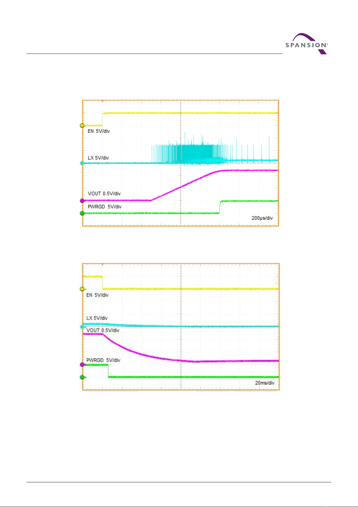
Figure 9-3 Start-up (EN=0V=>5V) VIN=7.4V,VOUT=1.2V,IOUT=0.05A, SLP_N=H
Figure 9-4 Shutdown (EN=5V=>0V) VIN=7.4V,VOUT=1.2V,IOUT=0.05A, SLP_N=H

O p e r a t i o n M a n u a l
18 MB39C502-EVBSK-01_SS901-00030-1v0-E, November 19, 2014
CONFIDENTIAL ver1.1
Figure 9-5 Load step response (VIN=7.4V,VOUT=1.2V) IOUT=0.05A to 7.69A, SLP_N=H
Figure 9-6 Load step response (VIN=7.4V,VOUT=1.2V) IOUT=7.69A to 0.05A, SLP_N=H

O p e r a t i o n M a n u a l
November 19, 2014, MB39C502-EVBSK-01_SS901-00030-1v0-E 19
CONFIDENTIAL ver1.1
Figure 9-7 Switching waveform (VIN=7.4V,Iout=8.54A) , SLP_N=H
Figure 9-8 Switching waveform (VIN=7.4V,Iout=0.05A), SLP_N=H
Table of contents
Other Spansion Motherboard manuals


