Stage Accompany PPE-2410 User manual

stageaccompany
PPE-2410
Programmable
Parametric
Equaliser
SERVICEMANUAL
Cont
ents
:
Safetyand
warranty 2
1.1 Safety 2
1.2 l{arranty ......2
Description
of the equaliser. 5
Takingthe PPE2410
apart.... 6
Basic
diagram. I
Basic
operationof the electronics .....10
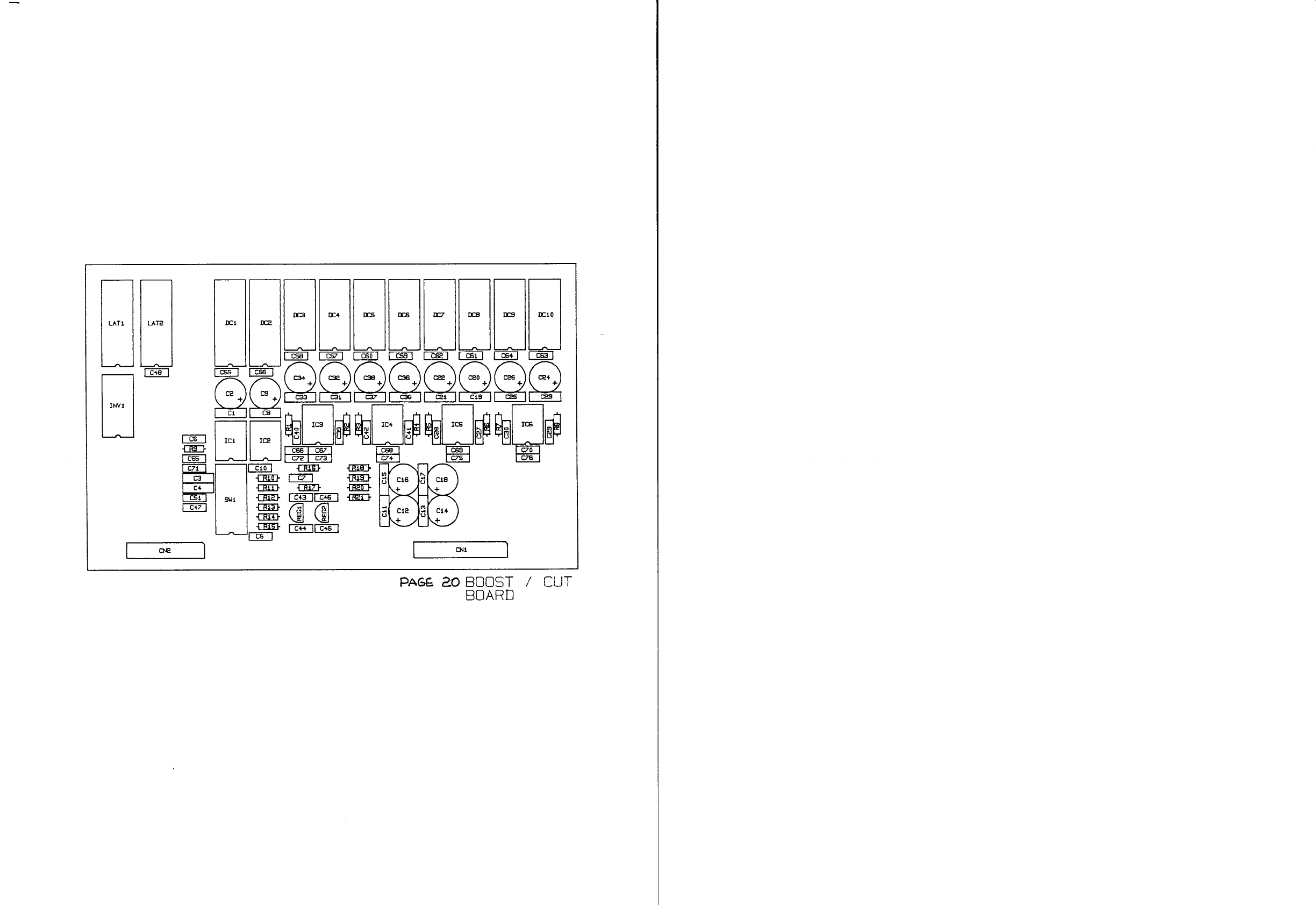
5.1 Theinput / output board .....10
5.2 The
boost
/ cut board ...11
5.3 Thefilter board ...12
5.4 The
clip andlevel detection board.
....14
5.5 The
processor
board.... ......16
5.6 The
front board.... .....16
5,7 Thefront control board ....,.17
5.8 Themother
board ...17
5.9 The
power
supplyboard .......17
Circuit layouts.... .....18
Basic
operatíonof the software.. ......45
Downloading
of the software.. .....51
Adjustments... .....52
Final tests ...54
Specifications. ,...57
Serial boost/cutboard
(supplement
1)... ....58
New
operationalamplifier (supplement
2). ... .....67
Power
supplyupdate
(supplement
3) .....68
This manual
containsconfidential information.
Anyform
of
duplication is prohibited !
2
3
4
5
6
7
8
9
10
11
t2
13
t4
page:
date:
issue
2I-r2-1988
1 Safetvandwarranty
1.1 Safety
-l{arning
Inside the PPE2410,
ACvoltages
up to 240V may
be present !
-Connection
to the mains
voltage
The
PPE
2410's
chassisis connected
to ground
by the grounding
conductor
in the pou,er
cord. To avoid electrical shock,
plug the
power
cord into a properly
wired receptacle.Víhenthis ground
connectionis not present
or interrupted, all accessible
parts of
the equaliser
can
causean electrical shock.
-Fuses
To avoid fire hazard,
only replace
fuses
by the same
type and
vaIue.
-Servi
ci
ng
Do
not perform
internal serviceor adjustmentsunlessthere is
another
person
present,
capableof renderingfirst aid and
reanimat
ion.
Try to perform
aII service
work
with mains
power
off. Remove
mains
plug to be sure that there are no internal voltages
present.
1.2 l{arranty
SUMMARY
StageAccompany
warrants
to the original commercial
purchaser
of
eachnew
Stage
Accompany
product, fromthe date of purchase
by the
original purchaser
until the endof the warranty
period, that the
product
is free of defects in materials
or workmanship.
WARRANTY
PERIOD
Thewarranty
period on all Stage
Accompany
products
is five years
from
the date of the first consumer
purchase,
with the exceptionof:
- all electrical products:
three years
fromthe date of the
first consumer
purchase;
- coneassemblies
in the loudspeaker
anddiaphragmsin the
CompactDrivers: Sl9g fromthe date of the first consumer
purchase;
PPE 24LO
SERVICE MANUAL 2
:I
PPE 24LO
SERVICE MANUAL
pa$e:
date:
issue:
3
2I-te-r988
I
- movable
parts, such
as castors, locks, handles,hinges, fans,
etc: one
year from
the dateof the first consumer
purchase;
- computers
and
associated
peripherals: six months
fromthe
date of the first consuÍner
purchase.
HOI{TOVALIDATE
THEWARRANTY
To validate víarranty,
fill out the enclosed
warranty
card and
return it to stageAccompany
within ten daysof the purchase
date.
The
purchaser
must
always
keepthe original bill of sale to
establish the date of purchase.
ITEMS
EXCLUDED
FRO}TWARRANTY
Appeal
on warranty
will be voidedin case:
of defectscaused
by influencefrom
the outside, accident,
misuse,
neglect
or influence
of water;
- the serial number
on the warranty
and/or
product
has
been
defaced,
altered or removed;
- of damage
due
to shipment;
- of damageresulting from
neglection
of instructions listed in
the user manual;
- of damage
caused
by incorrect, abnormal
or abuse
during
delivery;
- the unit has
beenrepaired
(or shown
signs of repair) by
someonenot authorised
by Stage
Accompany;
- if the warranty
registration card has
not been
returned
to
StageAccompany
within 10daysof purchase;
- the original bilI of sale cannot be presented
whenever
warranty
service is required;
the cause
of damageis unknown
IíHAT
ríE I{ILL DO
Shipment
of the product
to a StageAccompany
dealer is at the risk
andresponsibílity of the customer.
StageAccompany
will pay
all labour
andmaterial expensesfor all
repairs covered
by this warranty.
StageAccompany
will not pay the
cost of shipmentto the StageAccompany
dealer or to the factory.
However
StageAccompany
witl pay
the return shippingchargesif
repairs are covered
by the s,arranty.

PPE 24TO
SERVICE MANUAL
pa$e:
date:
issue:
4
2t-L2-1988
I
PPE 24IO
SERVÏCE MANUAL
pa$e:
date:
issue
6
eI-L2-1988
I
CAUTION
l{arranty
work
canonly be performed
at our authorisedservice
centers
or at our factory. Every
repair or attemptedrepair by a non
authorised
party will void the warranty.
StageAccompany
resêrves
the right to alter specifications without
prior notice.
3 Takingthe PPE
2410
apart
In most
servicing cases,it will be sufficient to remove
the
equaliserstop panel. After this you
will have
access
to aII the
boards.
First be sure that the mains
plug is removedfromthe receptacle.
Then
remove
the eight top panel
screwsand
four side panel screws
(fig 1). Nowthe top panel
canbe removedandthe motherboardwith
all the plug in boards
wiII be visible.
l'
L
rl'---
r,if
littl
illl
illl
ii L_
Fig 1 Topside of the ?PE2410
The
plug in boardscanbe taken
out just by pulling (fig 2).
Access
to the front andinput / output boardcanbe obtained
by
removing
the tv{o
screuísof the appropriate
bar at the side panels
the PPE2410.After removing
the bars the front or back
panel canof
be

PPE E41O
SERVICE MANUAL
page: 7
date: e1-Ie-1988
i ssue: I
taken out.
The motherboard
and the power
supply board can be taken out by
removingthe screwsthat lock themto the bottom panel. For the
power supply board an additional four screws that secure the power
transistors have to be removed
(see fig.3).
!]SPL,iY & 3!::!NS
Fis 2PPE2410 with removedtop panel
F
f
U
E
fl
F
-
o
c
m
-
F
f
TJ
F
f
tJ
F
o
o
h
T
U
z
F
U
UJ
F
U
J
UJ
U
4
n
J
tl
F
:
t)
É.
íl
É.
U
F
J
h
tu
=
IJ
F
U
tr
U
cí
F
-)
f,
=
U
PPE 24LO
SERVÏCE MANUAL
pa$e:
date:
issue
8
2r-1e-1988
I
tr
____t
.r
(+
-r
tl
+
o
o
Fig 3Power
supply details
lÈïÈiixl
tïo l.ErE-
I
EqIEIISI.J DIGIT^L
ATTE}.TXTOR
PROCESSOR
CIRCUIT FRONT
CONTROL
CTRCUIT DISPLAYS& BUTTONS
CLIP & LEVEL
DETECT
ION
DI6ITA. I DTCITAL
^TTENATTn ES_!5!L_ I ATTElr.nTm
+
ISANETI a
IOUT I a
rr +-tl
l..&*l-r ll qrrPurGND
( LrFr
I
ffii F
SAJ€Í GND
LIFT
IN
IMIDï
| qÍ
Íl€J
f-ïi--t
[-leËql
I
+
POWfR
SUPPLY MAINS
S\NI TCH
MAINS
FI LTER
BASTC
DIAGRAX PAGE
3

PPE
24TO
SERVÏCEMANUAL
page
date
issue
:
10
09-05-r
989
update I
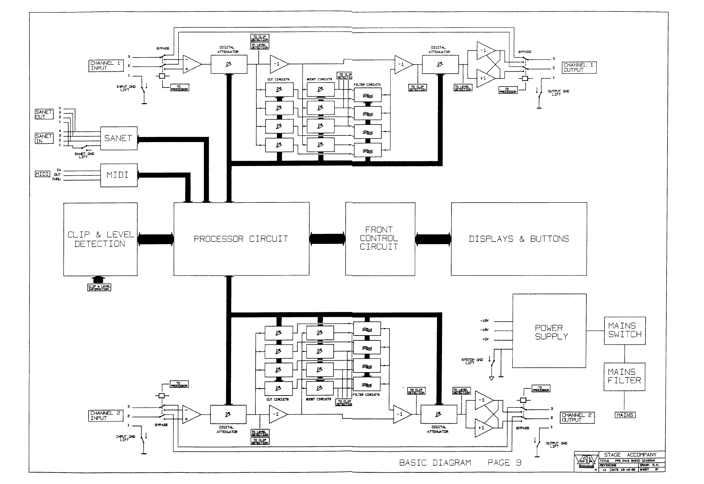
5 Basic operation of the electronics
This chapter describes someof the key circuits of the PPE2470. The
completecircuit drawingscan be found on page 18 to 44.
5.1 The input / output board
The input / output board contains the electronics for the input
amplifiers, the bypass
relays, the output amplifiers, the MIDI and
the SAnetconnections.
The input amplifier is a straightforward opampdifferential
amplifier.
The amplifier provides for a 3 dB gain. Common
moderejection can be
trimmedwith TR2for low frequencies and with TRl for high
frequencies. See
page
52 for the exact adjustment
procedure. The
value of R4 is three times higher than R5 to obtain the same
input
impedanceat the + and - inputs (24k0 each leg).
o{í $ttr
Fig 4 Input amplifier
Both inputs and outputs are equiped
with reiays to provide full
bypass in case the power
of the equaliser is turned off.
The outputs are electronically balancedand have
a DC
servo
feedback. This feedback
provides for a Iow output offset.
The outputs are cross-coupled so that a shortcircuit of one output
results in a 6 dB extra gain on the other (transformer simulation).
Output symmetrycan be adjusted with TRS
and TR6. See page 52 for
the adjustment procedure.
The output board also contains the digital interfaces.
A SN75176RS422
driver provides the SAnet
interface.
MIDI,
is only buffered and the controller is located on the processor
board
l'
PPE
24TO
SERVÏCE }'ÍANUIAL
page:
date:
i ssue
11
09-05- I989
: update I
OJTF1JT.
CTI1 OJTRJT
Fig 5Output amplifier
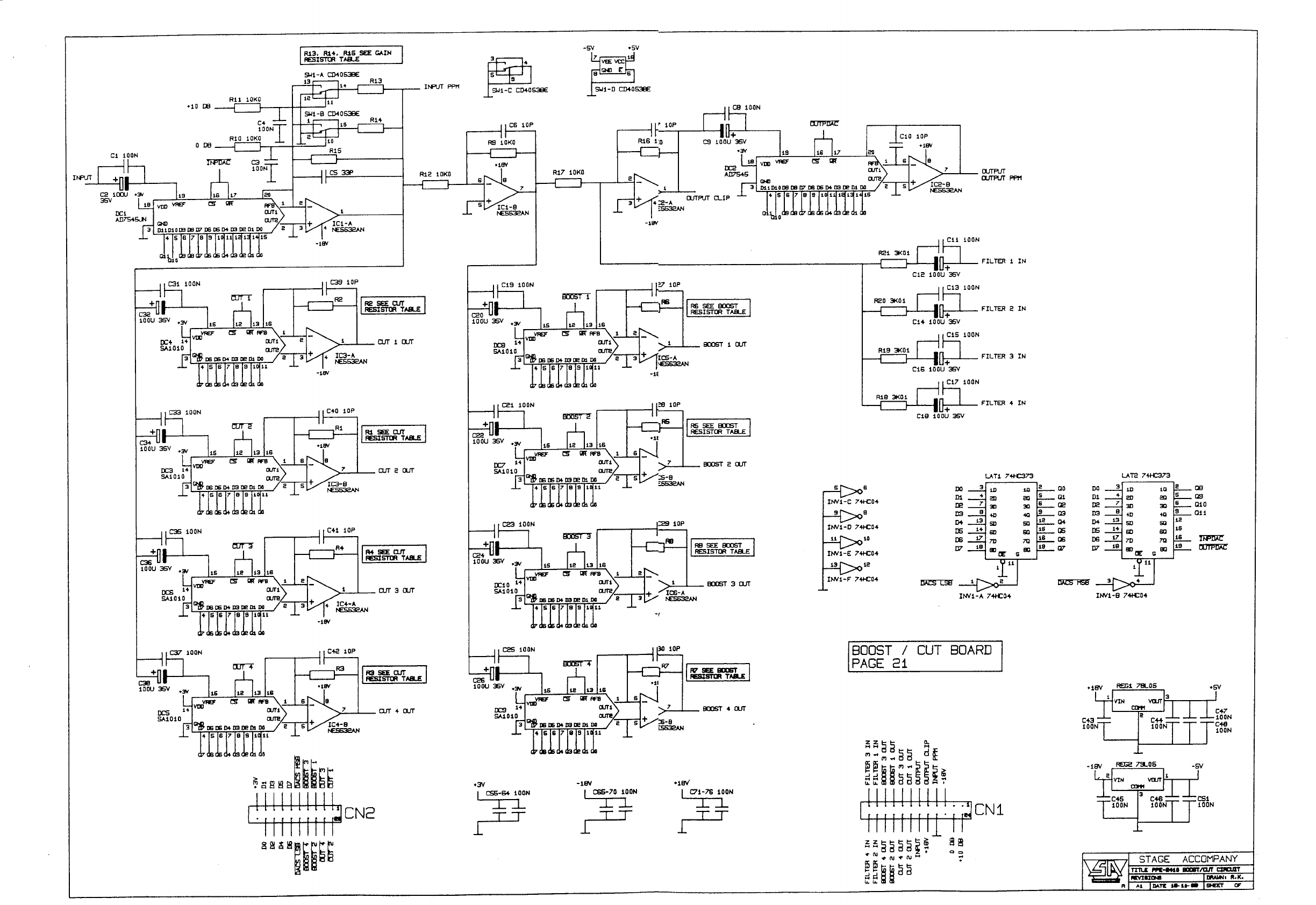
5.2 The boost / cut board
The boost / cut board contains the electronics to supply the filters
with the right amount
of signal and to add the filter output to the
original signal.
Each
of the two channels has its ownboost / cut board and figure 6
shows
the basic set up.
The input level is controlled by DCl and extra gain can be addedÍn
the feedback
network around
R13
and R14. The digital code at the
digital input of the DAC
determines
the attenuation of the circuit.
This level in dB can be calculated with the formula:
A=20*Iog n
4096
where n is the decimal value of the bit code. when
extra gain is
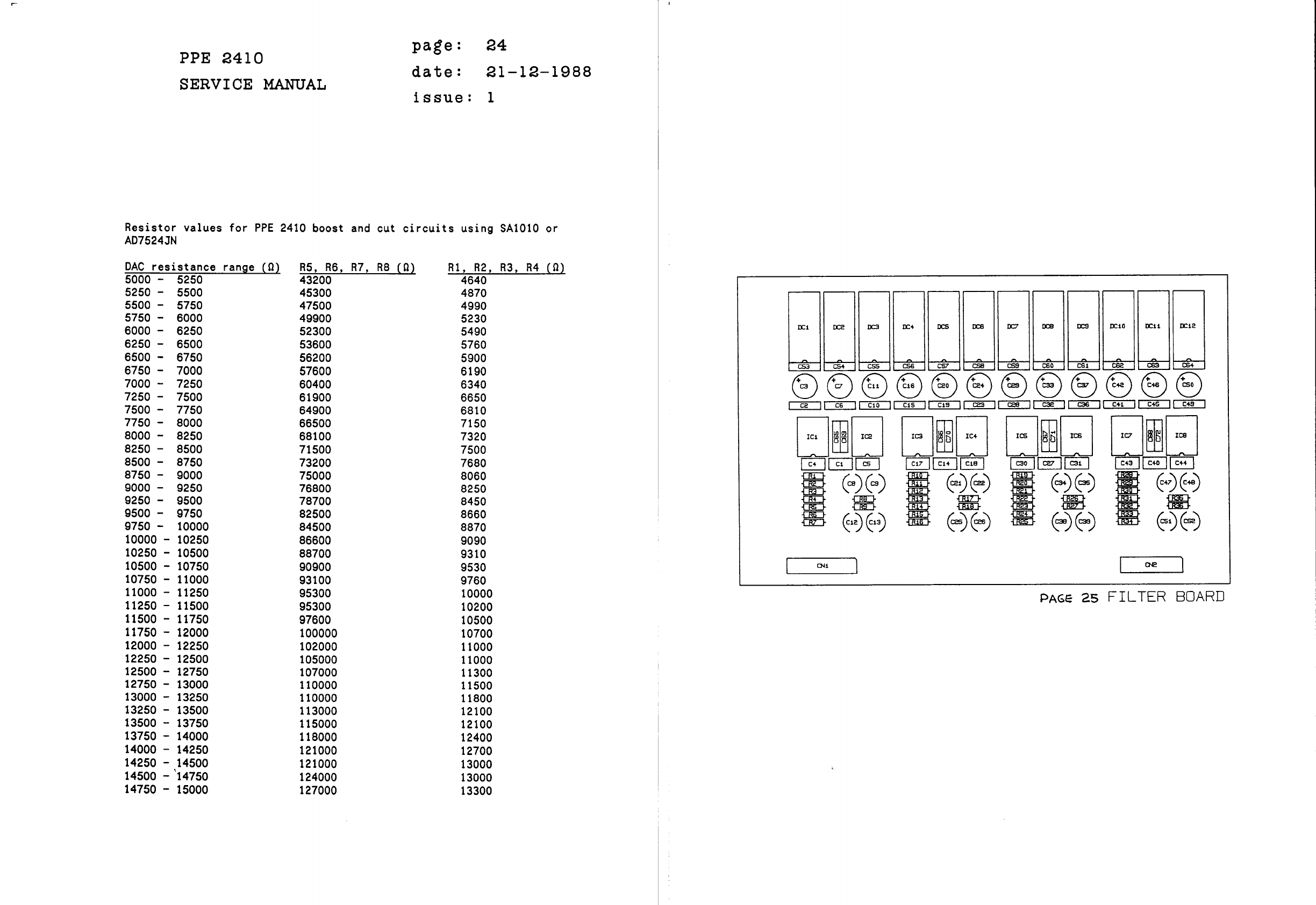
used, add 10 or 20 dB.
since the Ínternal resistance of the DA
converter influences the
overall gain of the circuit, R13, R14and R15
should be matched
to
the DA
converter. Page
22 contains a table where
the exact values
canbe found.
TheDAC
resistance
can
be measured
between
pins 1 and20 after
has
beenremoved
fromits socket.A condition is that you have
supply
the DAC
with a voltage
of 1.2V between
pins 3 (Gnd)
and
18 (vdd).
it
to
pin

PPE 24LO
SERVICE },!{NUAL
1e
09-05- I989
board and each board
7 shows
the basic
page
:
date:
issue: update I
FiS. 6 Boost / cut board set uP
Next the signal is fed to four DA
converters which provide the cut
signal for the state variable filters. In figure 6 only one (DC4)
is
shown
for the cut signal of filter 1. This circuit can provide a
gain factor of -0.89.
After inverting the signal with IC1-b, another four DAconverters
feed the signal for boost purposes
to the filters. The boost circuit
for filter 1 is shown
(DC8)
and this circuit can provide a gain
factor of 8.44,
Here again, aII the feedback
resistors have to be matched
to the
DAC.
The values can be found in the tables at page
24. The DAC
resistance can be measuredbetween
pins 1 and 16 after the DAC
has
been removed
from its socket. A power
supply is not necessary.
The original signal is added
with the filter outputs at the input of
ICZ-a. The polarity of the output signal of each
of the filters
determines
whether the signal is going to be boosted
or cut at a
certain frequency. The frequency is determined
by the filter
settings at the filter board
The output level is controlled by DCZ.
5.3 The
filter board
Eachchannel
contains four
configurat ion
is equiped
with its own
filter
state variable filters. Figure
of a state variable fi Iter.
Glu
Mtlr
PPE 24TO
SERVICE }ÍANUAL
pa$e
:
date:
issue
filter with DAC's
15
09-05- I
989
updat e
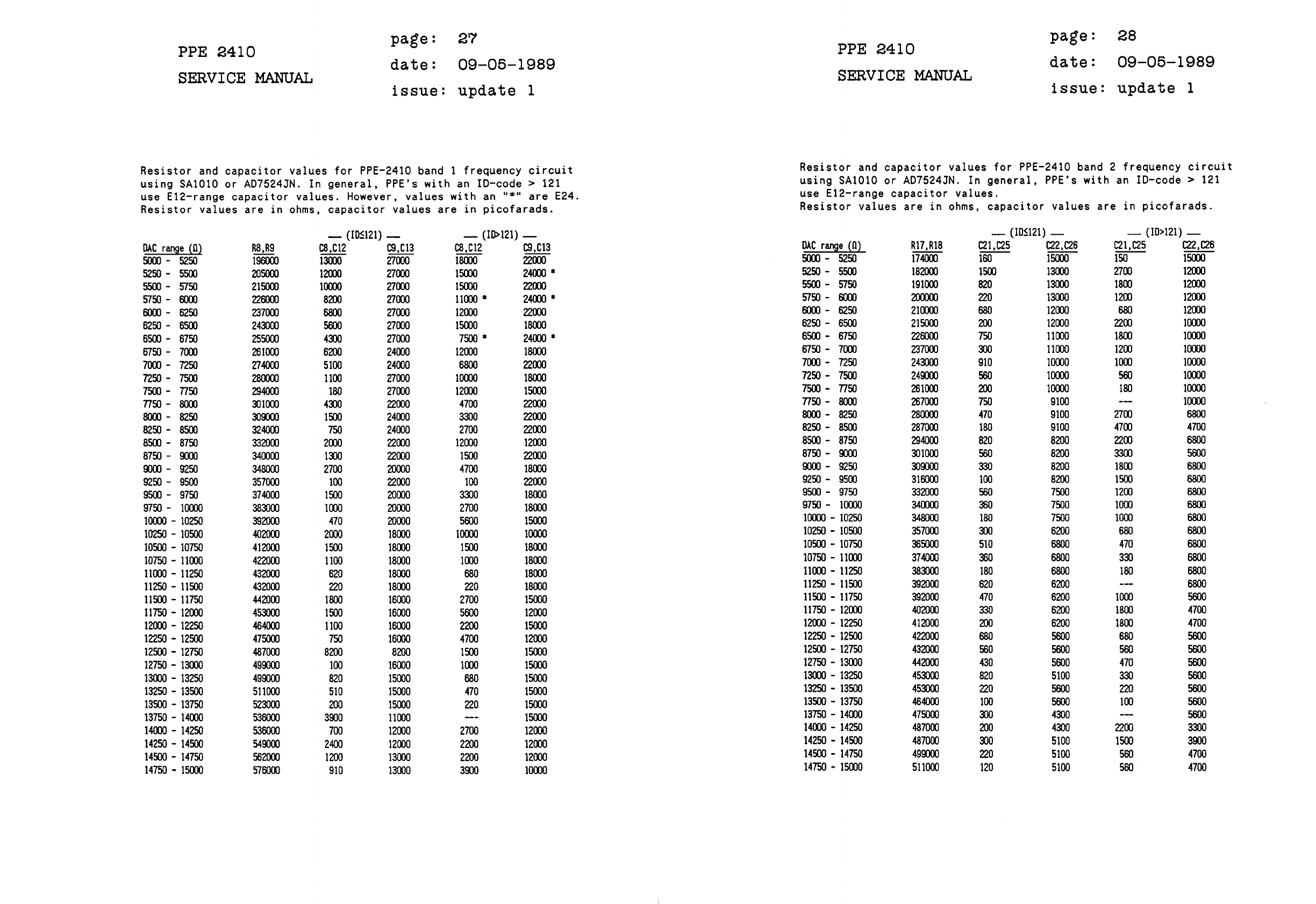
Fig.7 State variable
The boost and cut inputs (from the boost/cut board) are summedat
IC1-a. Next you find a circuit with 3 multiplying DAC's
and multiple
feedback. DCz
and DC3
are matched
and determine together with C9 and
Cl3 the center frequency
of the bandpassfilter. C9 and Cl3 are of
the samevalue. The centre frequency is given by the formula:
fc= 2.
where
Rdac
is the internal
digital code present at the
given by:
ntR6""'C
value of the DAC
digital input
). (which dependson the
The DACresistance is
Rdac :256
. Rfb
n
n Represents
the analogue
value of the digital code (oooooooo
= 0 to
11111111
= 255) and Rfb is the basic resistance of the R-2Rnetwork
inside the DAC.
The value varies between
5 and 1s k0 and the correct
values of the capacitors can be found in the tables at page
27.
DC1
determines
the O-factor and its value is given by:
o
Al
I resistors that
table at page
31.
=Rdac'R3JR4
nffiRT
should be matched
to DCl can be found in the

PPE 24LO
SERVICE MANUAL
page:
date:
issue:
L4
2L-L2-1988
1
5.4 The
clip and
level detectionboard
Themain
function of the clip andlevel detectionboard
(see
schematics
at page
33) is to interface analoglevels to the
microprocessor.
There
are two types
of interfaces, one
for Ievel
detection andone
for clip detection.
For the level detection, four analogue
signals (both the inputs and
both the outputs) are precision rectified (Fig 8) and
fed to an
analoguemultiplexer. After the multiplexer, eachof the DC
signals
is convertedin a digital code.
OIl IÀRJT
Fis.8 Precision
rectifier
The
AD
converteris built aroundIC1, IC2andIC3. After the
multiplexer the signal is passed
to a buffer andcomparator
IC3
comparesthe input signal with the reference
signal produced
by DA
converter
IC1. This reference
level dependson the digital code
produced
by the processor.
Bymeans
of succesiveapproximation,
the
processor
determinesthe digital valuewhich
is closest to the
analogue
level with the formula:
D=Uin*256
q_
D is the analog value of the digital code (00000000
= 0 and 11111111
= 255). U,o+ is the reference voltage (-10.24 Y) adjusted with Pl.
For the cIÍp detection, all possible places where
an overload can
occur are sensed
and fed to comparators.These
are:
The two inputs of the equaliser (an overload can occur when
10 or 20 dB extra gain is used).
- The four boost outputs of each channel (each filter can
provide 19.5 dB of gain).
PPE 24LO
SERVICE MANUAL
pa$e: 15
date: 21-I2-1988
lssue: I
Thefilter output summing
point (each
fÍlter can
provide
a
small amount
of boostat the samefrequency
causing
the
output to clip).
All signals are single sided rectified andattenuated6 dB
before
they are fed to the comparator.
The
comparatorhasoutputs on logic
level and
are interfaced to the data bus through74HC244
buffers.
ICl5 latches the control signals for bypass,input gain and
the
multiplexer.
PPE 24LO
SERVICE MANUAL
page:
date:
lssue
16
2L-12-1988
I
PPE 24LO
SERVICE }{ANUAL
5.7 Thefront control board
The
front control boardcontains
the drive electronics for the
displays on the front boardand
the circuitry to readthe position
of the switches.
All information
for the displays is sent serially to the front
board. Eachframe
contains
the informationfor onecolumn
(32 bits).
Eachtime data is written to a certain columnof leds or displays, a
read
anda write cycle is performed.
In the read
cycle, the "video int" level is lowand
the display data
is stored by the processor
into RAllIC9. The
processor
adressbuss
is passed
to the RAIIthrough
ICl andIC2. The
data contains32 bits
that are divided over 8 nibbles. The
data is stored into IC9
through
IC10-A.
In the write cycle, "video int" is high anddisplay control is taken
over completelyby the control circuit. TheRAl,{nibbles are
subsequently
loadedinto IC11
andserially transmittedto the front.
The
endof the cycle is detectedby ICS.
The
readout
circuit for the switches
comprehenses
IC12, IC13
and
IC14.
Thekeybuf
signals are normallyhigh. To reada row
of
switches,
oneof the keybuf
signals is madelow by the processor.
The
output of IC13
goes
low
andthe keycot
byte is transferred to
the data bus.
5.8 Themother
board
0n the mother
boardall interconnections
betweenthe various PCB's
are made.
It also containsthe decodinglogic for variouscontrol andchip
enable
signals.
5.9 The
power
supplyboard
The
power
supply
(page
43 and
44) is a straightforward regulated
supplywith 78 and79 series regulators.
The
5 volt supply
(mainly
for the digital circuitry) is extended
with a power
transistor to provide for a higher
current capability.
Its output is filtered to eliminate
processor
noise
out of the
supply
andmainsnoÍse
out of the processor
circuit.
pa$e:
date:
issue
17
2L-12-1988
I
5.5 The
processor
board
The
processor
circuit (see
page
35) containsa microprocessor,
power
down
protection, memory
and
the MIDI
controller.
The
processor
hasthree different kinds of on board
memory.
IC4 is
an EPROI'Iwhich
contains
the software
for starting the processor,
testing the other memories
anddownloading
the system
software.
IC3, a Flash
EPRO}I,
contains
the systemsoftware
andcanbe
programmed
through
SAnetwithout removingit.
ICSis a RALlwhich
contains
program
variables, e.g. the equaliser
control settings. This IC is provided
with battery backup
to save
the settings when
the mains
power
is switched
off. The
battery has
a life time of approx. 10 years.
IC7 and IC8 are protection IC's to save
is switched on and off.
IC6 is the MIDI controller which is the
MIDI and the processor.
0n the PCB,
R7and
C24are omittedand
Dl is replaced
by a 0 0
resistor. l{ith these
components,
the programming
voltage of the
flash EPROI/
canbe influenced.
5.6 Thefront board
The
front board
(seepage
37& 38) contains
the user interfaces:
buttons
anddisplays.
Boththe readout
of the buttonsand
the display drive are
multiplexed.
The
buttonsare scannedin the following víay:
AII keyrow
signals are normallyhigh. Keycol0 to 7 are normally
pulled'high'by the resistor networkA6. To read
a rorf,
of switches,
its keyrowinput is made'Iow'by the processor.
Every
button that
Ís pushed
causesa shortcircuit between
its row
and
its columnso
all of the columnsof the activated switchesare pulled low.
Unactivated
switchesIeavetheir column
high. AII keycol levels are
read
by the processor,
the next keyrowis made'Iow'and the same
procedure
follows. Bymaking
all the keyrow
signals subsequently
low, alI the buttons
are scanned.
The
displays are driven in a similar way.The
control logic on the
front control board
loadsthe data for a certain column
into the
shift registers IC3, IC4, IC7andIC1. After this is finished,
demultiplexerIC9
selects the right column.
Theregisters are Ioaded
again
aqd
the next column
is activated.
memory
contents whenpower
direct interface between

o
Í
,-* _q+
F-..'1Hr-
n Ë*lt ffi tln
lnl m
ffi-lul m
ffi
I lBffilnl I l-* rcr-r
ffit,lk"ffiE
{'-'-i
ffi-É
rd | Í Ë8.
Eg
@
Í---T-'l
ttl
l.l
t.Ft
l-,-]
I F-r
l*lol
l8lËl
lr
rEr-t
En
r-*-t f:-r
ffil = lol {EiirF
-l \ lNl
I ltcÍrtl_rl I
tttEttl
lËl lël ra6-f lËl
I'l t3 ffiií_l'" I
I tBelg|t I
- u4
1.gr | .. |rnrrr.
ffilË lË
i--' ffi=*
l{
tnl
tgt
lt
p
l|l
F
@
TnH
11 z_
>JJ
;U
L'
[J --r
o
C
-{
-U
-
--l
ct
t00u
I
I
J
fro
DATA
9qJ€T 5V
SAJ€Í.
s^l€T-
s^r€Í GNI) R.r3
b1Ê
hra
1t.l.t1{€
Rtl !0K0
Rle g(( CN3
c}lt SYPA.SS .5
I
tl
lr Í-l re I
?
6r
sAr€T-
9À|€Tr
sA|€T 5V
SAT€TGND
D1
l|l,ttr€
m
1|l411€
R,r 30K1
FÉBTOT
.IFs
a<
10r R30 11100
R5 10K0
TE
tt.l4t4€
D+
t|r414€
-'*l Ic+
Uá'
É
17P c}It Ii€TJT CHT
o'JTruT
,.5
tl
I' fk_J
tl
r
í'1'€**
''tl-Tèto
4e?'5
FF
tt
22
-ï-Ï-l-
ttrt;t;tl
llllll
-,Lvhvqv
íí
\h
dd
qJt
do
O€ IIft'T C}E OTPUT
-l8\t/
ffIz t0x0
t/ ct7-ee t00N
T=_
-r -r
7
| --ag roox
-:n_ INPUT/ OUTPUTBOARD
PAGE13
I
I
)I
Feft t0K0
ro-f RlF tn00
cr4-r8 r00N
CN1
FÍ'
Iro
t-ln
l*ll*,,1
till
L^IL^J
rtrl rÉ-l
.JA
\ *,\ *:
I ces ll c23 I
A rt1
WHffi
fEo I
lvo I
till
l*ll *l
lill
l-l l-J
rEI TE-fl
í)íJ
\ .:\ .:
I c21 ll cls I
À*
ffi[_]#
r6t
luo I
nt-t
l*ll*l
L^-]L^_l
lGo-l l-E-l
@@
l@llcsl
till
l*ll--l
lill
l-ll-J
fcsol I csrl
Aí}
\ .:\ .i
I ca3 ll cal l
ÈÉ
H[:Jffi
IGTFI
@@1
ftiEl {
rFt t
{32} t
rc13
lfcl€ | {
GG
I c+1 ll-EFl
t--lt-l
l-'ll-l
L_lL^_l
ltsll.9l
oo
I cr ll c8 |
EE
itn
fln
Ercl€r
PAG AOBOOST / CUT
BOARD
RI3, R14, RTE SEE GIIN
RESIST6 ÏAsl
5rJ1-^Cl}+osg
13 II.fUT PPí
100NI
I
0K0 Ics 100u35v
r00N
I
IR1? 10K0 Rtz 10K0 OJTPUT
dJTPtJT PPí
Ce 1UJ .3v
35v I
E1
AllzgS,ll
IC1
-B
r€554€AN
ICl-A
f€sselx cll 100N
R21 3<01 FILTER 1 IN
cia 100u5v
c19 100N c13100N
F20A<01 FILTER A IN
c?0 u.
100u
35/ cl+ 100u3sv
c15 100N
oJT 1 qÍ IrA
sAl010 rcffir I oJT
FILÍER 3 IN
lu+
c16t00usv
rua 3<01
ce1 100N FILTM + IN
tr33 100N c+010P ffiT-e cla 100u3sv
l'2?
r00u
sv .1'
100u
35v .3/
wl
sAÍ
0t0 ffir e cuT
E3 14
sA1010 CUÍ ? qJT
f.€55:€^fi m
D1
ÍE
EGI
It4
E
D6
trl
010
:FUC
d]ï"trE
IÀMI-D Z1+C0,r
7
B
t3
I
,z
IWI-E Z.ífco,l
G
t00u
sv .3'
m6r 3 qjr ItJVl-F Z.+|'Co.t ME-trSd MFËd
ctJT3 qJT
c3z 100N c25 100N BOOST
/ CUTBOARD
PAGE
A1
c26
t00u 5v .3|/
C1JT+ OJT DcÍ} t+
s^l 010 mosl I ott
tc.l-B
r.rE56:IarN
Od
.q *-,ËHEËE ÍiFl:s
à6
SHssË;EEEr
+1-]$-I+cNe
tfttÍlilr- I csE-et !00N
-T-
-rT
I
cst
r00N
E
sÁ
8ËHHEË :í!:?:Ee
::
FEBH55
rr?
All7É+s IC?-8
f€sse^N
ÍlTDtÍ)IE ÍE IP IE !6 D4 lr} IE OTDO
Ic:I-A
t.€5SeAN
Dc6 l+
9À101
0IC+.4
NES53e^N
5r\ -5
Irwl-c z4fc0,í
!'Tt 7+€373
Ifwt-A z,tlEo+
ltt rE
?,Jeo
3tI
+D {o
5D 5D
6D €O
mm
-E c-
TJ'T?71+€3,73
DO
D1
m
v+
K
D6
w
+
7
I
t3
*
L7
18
!! 10
a4
Í'I
.+D 10
SD 5D
60 €o
mm
-E "-
.rsV
CN1
STAGE ACCOMPANY

PPE 24LO
SERVICE MANUAL
page3 22
date: zL-Ie-1988
issue: I
P?E-2410resistor valuesfor input gain circuit usingAD7545JN
DACresistance rglga(!,)
5ooo=-5Z5o
5250- 5500
5500- 5750
5750 - 6000
6000- 6250
6250- 6500
6500- 6750
6750 - 7000
7000 - 7250
7250 - 7500
7500 - 7750
7750 - 8000
8000- 8250
8250- 8500
8500 - 8750
8750 - 9000
9000
- 9250
9250
- 9500
9500 - 9750
9750- 10000
10000
- 10250
10250
- 10500
10500
- 10750
10750
- 11000
11000
- 11250
11250
- 11500
11500
- 11750
11750
- 12000
12000
- 12250
12250
- 12500
12500
- 12750
12750
- 13000
13000
- 13250
13250
- 13500
13500
- 13750
13750
- 14000
14000
- 14250
14250
- 14500
14500
- 14750
14750
-'15oOO
15000
- 15250
15250
- 15500
15500
- 157s0
R13
(
0'l
23700
24900
26100
27400
28000
29400
30900
31600
33200
34000
35700
36500
37400
39200
40200
4t200
42200
43200
44200
45300
46400
47500
48700
49900
51
100
52300
53600
54900
56200
57600
59000
59000
60400
61900
63400
64900
64900
66500
68100
69800
69800
71500
73200
R14
(0)
5620
5900
6190
6490
6810
6980
7320
7500
7870
8060
8450
8660
8870
9310
9530
9760
10000
10500
10700
11000
11300
11500
11800
12100
12400
12700
13000
1
3000
1
3300
13700
14000
14300
14700
14700
15000
1
5400
1
5800
15800
16200
16500
1
6900
16900
17400
R15
(0)
51
100
53600
56200
59000
61900
63400
66500
69800
71500
73200
76800
78700
82500
84500
86600
88700
90900
93100
97600
100000
102000
105000
107000
110000
113000
115000
118000
118000
121000
124000
127000
130000
133000
1
33000
137000
140000
143000
143000
147000
150000
150000
154000
158000
15750
16000
16250
16500
16750
17000
17250
17500
17750
18000
18250
18500
18750
19000
1
9250
19500
19750
16000
16250
16500
16750
17000
17250
17500
17750
18000
18250
18500
18750
19000
1
9250
19500
19750
20000
73200
75000
76800
76800
78700
78700
80600
82500
82500
84500
84500
86600
86600
88700
90900
90900
93100
17800
17800
1
8200
18200
18700
19100
19100
19600
20000
20000
20500
20500
21000
21000
21500
21500
22r00
PPE 24LO
SERVICE MANUAL
pa$e: 26
date: e1-12-I988
l ssue
: I
158000
162000
165000
165000
1
69000
174000
174000
178000
178000
182000
182000
187000
191000
191000
196000
196000
200000
PPE 24LO
SERVICE MANUAL
pa$e: 24
date: eI-Lz-I988
lssue: I
Resistor
valuesfor PPE
AD7524JN
DAC
resistance rangx
(!.)
506,o.'-
s25ó--
5250
- 5500
5500 - 5750
5750 - 6000
6000- 6250
6250- 6500
6500- 6750
6750 - 7000
7000 - 7250
7250 - 7500
7500 - 7750
7750- 8000
8000- 8250
8250- 8500
8500 - 8750
8750 - 9000
9000
- 9250
9250 - 9500
9500 - 9750
9750- 10000
10000
- 10250
10250
- 10500
10500
- 10750
10750
- 11000
11000
- 11250
11250
- 11500
11500
- 11750
11750
- 12000
12000
- 12250
12250
- 12500
12500
- t2750
12750
- 13000
13000
- 13250
13250
- 13500
13500
- 13750
13750
- 14000
14000
- 14250
14250
- 14500
14500
-'14750
14750
- 15000
2410
boostand
cut circuits using 541010or
R5,R6,R7, R8
(0)
43200
45300
47500
49900
52300
53600
56200
57600
60400
61900
64900
66500
68100
71500
73200
75000
76800
78700
82500
84500
86600
88700
90900
93100
95300
95300
97600
100000
102000
105000
107000
110000
110000
113000
115000
118000
121000
121000
124000
1
27000
R1, R2, R3, R4
(0)
4640
4870
4990
5230
5490
5760
5900
6190
6340
6650
6810
7150
7320
7500
7680
8060
8250
8450
8660
8870
9090
9310
9530
9760
10000
10200
10500
10700
11000
11000
11300
11500
11800
12100
12100
12400
12700
13000
13000
1
3300
HHHHHHHHHHHH
ooo@@@@@@@@@
l--] f--l f€10-1 f€-i-] f€t-á-l lE] fE-f lEl fé-l Írl fr| frrl
ffi @(-")
ffi @e)
rETÍ1 ÍÉT'1 Tffi JT'ta
cií @ @ GÈb
ffi e)e) ffi e)e)
ffi í.")í*)
GDl. \./ \,/
Effi
{E /\/\
{:D (',, (''
f *'_l
ffi (r(t
ffiffi
ffi G)e)
f--""--l
rc5 TT-]
l^l-l
tl] IC6
É^ @
PA6E
?5 FILTER BOARD

ffiT! IN
IN w 3Ét<e,
Rl,+
Rll, R13. R14 S€E
o-FAcTm ÍAa-E
R11
R15 3a<2
UST ê IN
R16 g€
CUÍ ? IN
FaO, @. FE3 S€E
o-F^clu rAa-E
R21 g(e
msT 3 ÍN
Res3a€
OJÍ 3 IN
F€Í , EIT, F!Ê SEE
o-FACTTR ïAS-E
RÍB -I€
GT.I IN
F3+ -t€
CUÏ .+ IN
cl, c,+,c5, c!1. ct7, cta,
W. c30, c:ll, C,to, C+3, C,++
OI1ITTED
li.l.PP
FTUTP
FIFFF
HHHËrss;È '3í
f^l^ppgÁgE
l"l-f"l-
FFFF
LTLJ!LJ
IthlrlÀ
I cs3-6.í 100N
-T_
€;à^ |--Jfl|J '1 l,' 1,"1,"
l,E | - .'i
el -\ Icír rn0il a I l._vEF CS FFs \ r l 6l-\le
rE1 t*l'* oÍ1\ | \J rre t'í
SA1or0
sl orz,/ l, -/ s^l010
3
41ta*^ JHf.f"f,W++/TElzlEá*""' tE lts tN tlt IE tll t!
Ca3 l00N rrLr c F
c16 roou rv lJ;/E Ei ffi ffi \1131_\LE lC20 t00U 5\/
Dc+ r.l'* ort\ I :_ZJ E ,+
9\r0ro I anre/ l. -/ 5^1010
c3,r :_ rr Êt
casl I rrGtooN frLl.JF I Lrclrl
ceg 10ou gv Ll.-ye E ffi FFE \4_gl_\E lC3 100U Sv
De rl'* dÍt\ | \ZJ G 1'+
s^101o I m/ l. -/ s^lolo
á1:4,€ê^ lElgF=F=?tF=+++JE-f
{ZI&*,
Rrg 10K0
C.€ roru gv LJ-.|E cs tn FE ÉL ï-\: lc1'6 10ru 5tÍ
Htg,o,.l il:) l, ,> siÊ,o
Srso.reeor oo
STAGE ACCOMPANY
RS. R9. CE, C9, Cle, C13 S€E
BAr.4l ! FREII-EICí ÍAA-E
c10 100N
c1l 100u35V
FILTER 1 o.JT
RtZ, R18, e.!, @., .2S. Cê6 s
8^}O e FREA,€|CY ïA.A-E
FILTER A qJT
@, re7, C3+, G, G, C3€l
SEE
EAMI3 FREA-EIے TAA-E
s t00N
FILTER 3 OJT
&\]€ .t FRECIEICY TAS_E
c,tg 100N
c50t00u 5v
E1a l.
s^l01 0
FILTER 1 OJT
F[ï-rF
rILI J F
FIEÏTE
ILC-E
r.€sssêAN
tsF
z=BB
zz*-aru
HFtru
..rrE6
FStHHFF
zzzzÈÈ
HHHH55 ÁÁ
o-mí-- Í'í
adHHnn
Ëd55
44
ÈFILTERBOARD
PAGE
E6
rl8i/
issue: update I
Resistor and capacitor values for PPE-2410band 1 frequency circuit
using SA1010or AD7524JN.
In general, PPE'swith an lD-code > 121
use E12-range
capacitor values. However,values with an "t" are E24.
Resistor values are in ohms,capacitor values are in picofarads.
PPE 24LO
SERVTCE }A{NUAL
page
:
date: 2Y
09-05- I
989
- (rDrzl)
-
c8,cl2 B,cl3
t8m0 m
m
18m0
l5m0
m
27n
zffi
tm
3Sl
PPE24LO
SERVÏCEMANUAL
page
:
date
:28
09-05- I989
t)ACrange
(0)
50m
- 52s0
52s0
- sm
55m
- 5/50
5/s0
- 60m
60m
- 6250
62s0
- 6sm
65m
- 6750
6'7$- 70m
7m- nfi
nfi - 75m
75m
- nfi
7750
- 80m
80m
- 8250
8250
- 85m
85m
- 8750
8750
- Sm
sm - 92s0
9250
- 95m
gsm
- 9750
97$- 10m0
10m0
- 10250
10250
- 10500
10500
- 107s0
10750
- llm
11m0
- il250
11250
- 11s00
11s00
- 11750
117s0
- l2m0
12m0
- 122s0
122s0
- 12s00
12500
- 12750
12750
- 13m0
13m0
- 13250
13250
- 13500
t35m
- 13750
13750
- 14m0
r4m0
- 14250
14250
- 14500
14500
- 14750
14750
. 1500
- (rDslzr)-
6,C12 C9,C13
l3m0 nw
R8,R9
19m
a50m
2150m
zffi
a7ffi
2430m
2550m
2610m
n40m
am
a4m)
3010m
30m
3240m
33m
34mm
3480m
3570m
37CIm
3ffi0m
3920m
4020m
4120m
4m
€20m
€20m
44?fm
4$0m
4640m
4750m
487m
49Sm
49Sm
5110m
5z30m
$60m
$60m
54W
5620m
Í/60m
12m 27m 15m0 2,m0
'
lcÍttr nw 15mr m
8m nw llmo
. 24m
'
68m nw l2m0 m
5600 27m0
4300 nm
6200 24m0
slm 24m0
llm ?7m0
180 27mÉ
4300 m
1500 24m0
750 24m0
2m zffi
1300 m
2700 20m0
100 m0
1500 20m
tmo 20m0
470 20m0
2m0 18m0
1500 18m0
1100 18m0
620 t8m0
m t8m0
18m 16m0
1500 16m0
820 15m0
510 15m0
m 15m0
3S0 l1m0
7m Pmo
24ffi 12m0
12m 13m0
910 13m0
t5m0 18m0
7500
' 2,m0
'
l2m0 18u)
6800
10m
l2m0
47m
3ffi nw
27N m
12m0 l2m0
lsm 2ffi
47m 18m0
100 m
3300 l8flx)
27ffi 18m0
s600 l5m0
10m0
1500
1m0
680
n0
27ffi
5m
10m0
l8m0
18m0
l8m0
18m0
15m0
l2m0
15m
680 15m0
470 15m0
n0 l5m0
1sffn
um0
12m0
l2m
l(m
MC
rarue
(0)
5m - 5250
5250
- 55m
55m
- t/50
Ír50
- m
60m
- 6250
6250
- 65m
65m
- 6"/s0
6750
- 70m
70m
- nn
nfl - 75m
750- nn
nfi - 80m
80m
- &50
8250
- 85m
&5m
- 8750
8750
- Sm
sm - 9250
92Í]
- 95m
95m
- 9750
9750
- lmo
lmo - 10250
r02s0
- 10500
10s00
- t0zso
10750
- ltm
llm0
- 11250
il250
- 11500
115m
- ll7s0
11750
- l2m0
l2m0
- 122s0
12250
- 12500
12500
- 12750
12750
- 13m0
13m0
- 13250
13250
- 13sm
r3s00
- 13750
13750
- r4m0
l4m - 14250
14250
- l4sm
14500
- 14750
14750
- rsm
180
27m
47n
m
33m
8200 r8m
82m 15m
75m 12m
7500 lom
7s00 tom
6200 680
6800 470
6800 330
6800 180
6200
6200 10m
6200 l8m
6200 t8m
5600 680
5600 560
Rl7,
R18
174(m
1820q)
1910m
20mm
21mm
2150m
nffi
?37cm
2430m
24Sm
2610m
2670m
amm
2870m
2940S
3010m
30$m
3160m
3320m
34m
3480m
357m
3650m
37400
3$0m
39Am
3920m
4020m
4120m
4m
€20m
44am
4$0m
4$0m
46{0m
4750m
4870m
4870m
49Sm
5t1m
1100 16m0 m t5m0
750 16m0 4700 12m0
8200 8200 lsm
100 16m0 lmo 15m0
300
m3S)
4700
4700
Resistor andcapacitorvaluesfor P?E-2410band
2 frequencycircuit
using SA1010or AD7524JN.In general, PPE's
with an lD-code
> 127
useE12-range
capacitor
values.
Resistorvalues
are in ohms,capacitor
values
are in picofarads.
- (r0sr2l)
-- (IDl2r)
-
issue
: update 1
v2,e6 Pl,c25
15m0 t50
l3m0 27n
l3m0 18m
t3m0 lzm
t2m 680
r2m0 2n
t1m0 18m
1lm0 lzm
10m0 lom
10m0 560
330
100
560
360
180
300
510
360
180
620
470
330
200
680
560
300
m
120
c21,C25
160
l5m
820
m
680
200
750
300
910
s60
m 10m0
750 9100
170 9100
180 9100
820 8200
560 8200
430 5600 470
820 5100 330
msmm
100 5600 lm
4300
4300 nm
5100 lsm
5100 560
5100 s60
w,m
15m
l2m0
12m0
12m0
12m0
10m0
10m0
lm
r0m0
r0m
10m0
t0m0
6800
4700
6800
5600
6800
6800
6800
68ff)
6800
68fl)
6800
6800
6800
6800
5600
4700
4700
5600
5m
s600
5600
5m
5m0
56fl)
3300

PPE 24LO
SERVÏCEMANUAL
pa$e
:
date: 29
09-05- r
989
- (rD12l)
-
DAC
rarge
(0)
50m
- 5250
5250
- ssm
55m
- tf50
5'/50
- 60m
m - 6250
6250
- 65m
6m - 6750
67s0
- 70m
70m
- nfi
nfi - 75m
75m
- nn
nfi - 80m
80m
- 8250
8250
- 85m
85m
- 8750
8750
- Sm
sm - P50
92s0
- 95m
95m
- 97s0
9750
- 10m
1m0
- 1m50
1m50
- 10s00
10s00
- 10750
10750
- 11m0
1rm0
- 112s0
11250
- 11500
11500
- 11750
11750
- 12m0
ftffi- tm
t?2f0-nffi
12s00
- 12750
12750
- 13m)
13m0
- 13250
13250
- 135U)
13sm
- 13750
13750
- l4m0
14m0
- 14250
14250
- 145m
14sm
- 14750
14750
- 1sm0
- (rDsl2r)
-
c34,c38 85,c39
910 30m
r30 36m
n0 33m
110 33m
n0 ím
150 30m
330 27m
mnfi
110 27n
510 m
4$ 2n
1Í) ?4ffi
n0 2n
390 2000
130 m
750 15m
200 nm
130 20m
270 18m
430 r6m
180 18m
130 18m
390 15m
2n l6m
m l6m
160 lm
130 l6m
390 r3m
150 lsm
120 lsm
390 12m
360 12m
330 12m
200 13m
270 r2m
1s0 13m
lm 13m
100 13m
270 llm
150 t2m
R26,M7
20som
215m
?ztw
8m
2430m
255m
2610m
274ffi
28m
a40m
3010m
30m
324m
$20m
34mm
3480m
3650m
3740m
3830m
3920m
40m
4120m
4m
$m
44ntr
4$0m
4640m
4750m
4870m
4870m
49Sm
5110m
5z30m
$60m
$60m
54$m
s620m
5-/60m
5/60m
smm
qg
10m
2m
tn
560
470
330
m
ln
470
3g)
270
12m
tm
470
3g)
270
m
180
tm
3S
330
560
m
180
150
tm
3S
560
330
270
270
m
3S
180
150
c35,C3g
39m
nm
33m
33m
nn
nm
nm
nm
nn
nn
nn
n8
m
l2m
m
18m
m
18m
18m
18m
t8m
l8m
15m
15m
l8m
12m
15m
15m
l5m
lsm
nn
10m
l2m
l5m
l2m
t2m
12m
l0m
t2m
t2m
issue
: update t
Resistor and capacitor values for PPE-2410
band3 frequency circuit
using 541010
or AD7524JN.In general, PPE'swith an lD-code > 121
use E12-range
capacitor values.
Resistor values are in ohms,
capacitor values are in picofarads.
PPE 24IO
SERVTCE
MANUAL
page: 60
date: O9-05-I989
issue: update I
Resistor and capacitor values for PPE-2410
band
4 frequency circuit
using SA1010or AD7524JN.In general, PPE'swith an lD-code > l2l
use E12-range
capacitor values. However,
values with an "*" are
E24.
Resistor values are in ohms,
capacitor values are in picofarads.
t)AC
rarue
(0)
50m
- 5250
s250
- 55m
55m
- t/s0
5/50
- 60m
m - 6250
6'250
- 65m
65m
- 6750
6750
- 70m
70m
- nfi
nfi - 75m
75m
- nn
nfi - 80m
8m - 8250
&50
- 85m
8sm
- 87s0
8750
- Sm
sm - 9250
9250
- 95m
95m
- 9750
9750
- 10m0
10m0
- 10250
10250
- 10500
10500
- 107í)
10750
- 11m0
llm0
- 11250
11250
- 11500
11500
- 117i)
11750
- 12m0
12m0
- 122s0
12250
- 12500
12500
- 12750
12750
- l3m0
t3m0
- 13250
13250
- t35m
l35m
- 13750
13750
- l4m0
l4m0
- 142S
14250
- 145m
14500
* 14750
14750
- 15m
R3s,R36
l6m
1780m
1870m
1910m
20mm
2lmm
2150m
z60m
ziam
2fiom
24Sm
2610m
2670m
2740m
28mm
a40m
301m
30$m
31ffi
?4m
3320m
34mm
3480m
357m
3650m
3740m
3$0m
39Am
4020m
40am
4120m
4m
€20m
44nm
4$0m
4$0m
4640m
4750m
4750m
4870m
c47,C51
390
100
180
180
150
150
270
120
t20
100
m
1s0
c48,62
120
15m
l2m
l2m
t2m
l0m
l0m
t0m
10m
100
680
560
10m
680
470
680
560
680
680
680
680
680
560
560
3S
560
470
680
560
470
470
470
470
3g)
470
470
470
560
330
3$
- (r0s12l)-
c47,C5l C48,C52
n0 l3m
m 13m
240 12m
n0 llm
lm 12m
n0 10m
t20 llm
180 lm
130 lom
180 910
150 910
tm 910
24fr 750
150 820
r20 820
160 750
130 7Íl
110 750
160 680
200 620
t?0 680
lm 680
200 560
120 620
110 6A
150 560
130 560
120 560
110 560
180 470
130
120 510
510
110 510
130 470
120 470
110 470
100 470
130 430
tm 430
110 430
- (rDl21)
-
m
180
120
n0
20
180
120
100
390
470
270
470
n0
330
180
r50
150
tm
100
m.
180
330
150
n0

PPE 24LO
SERVICE MANUAL
Resistor values
for PPE-2410
Q-factor
AD7524JN
pa$e: 51
date: e1-L2-1988
issue: I
circuit using 541010or
R4, R22,R13, R14
R32
DAC
resistance
range
(0)
5000- 5250
5250- 5500
5500- 5750
5750 - 6000
6000- 6250
6250- 6500
6500- 6750
6750 - 7000
7000 - 7250
7250 - 7500
7500 - 7750
7750 - 8000
8000- 8250
8250- 8500
8500- 8750
8750 - 9000
9000- 9250
9250- 9500
9500 - 9750
9750- 10000
10000
- 10250
10250
- 10500
10500
- 10750
10750
- 11000
11000
- 11250
11250
- 11500
11500
- 11750
11750
- 12000
12000
- 12250
t2250 - 12500
12500
- t2750
t2750 - 13000
13000
- 13250
13250
- 13500
13500
- 13750
13750
- 14000
14000
- 14250
14250
-'14500
14500
- 14750
14750
- 15000
R2.R11 R29 R5. R23 R31
255000
267000
274000
287000
301000
316000
324000
340000
348000
365000
374000
383000
402000
412000
422000
432000
453000
464000
475000
487000
499000
51
1000
523000
536000
549000
562000
576000
590000
590000
604000
619000
634000
649000
665000
665000
681000
698000
715000
715000
732000
16900
17800
1
8200
19100
20000
21000
21500
22600
23200
24300
24900
26100
26700
27400
28000
29400
30100
30900
31600
32400
33200
34000
34800
35700
36500
37400
38300
39200
40200
40200
41200
42200
43200
44200
44200
45300
46400
47500
47500
48700
EËïBH#Ë%FEm'ffiffi-
nr--t t;il---l
Erl
'* ItL'"-:1EEEHffiffiBEEEffiw
Ei-
* lffiHEjF-uEl
""lul;lul
* .i
ffi EEfl-
HHHHffiffiffiffiHEffiWffiffiW
\-^.-/
@@d$
ue
BH
gH
ffi
HËffiffi
ffi
ffi
ffi
ffi
HH
l---- "" Il---'-_-l
CLIP & LEVEL
PAC.,E
32 DETECTIONBOARD

RI
4.lE tc6-A 74t814
1! {5474 T3 EI9+ZS 1+
R30+r?s
ICS-A LF*;!N
FÍF +ZsE
Ctll floD8
c}{1 0D8
c|e 'l0D€
o€ oDa
P1
10x
107
I I c+o-+3
Ic+z I roPN ,
1100N I I
Dt7
IC+-B r.-É-3S3.1
rcs-B rf3s3Í.1
IC8-9 LF3S3N
rca-A LF3s:ll
te IC1E UGFN
.16r'
ICl.t U{rFl
.1Ê|r'
.tw
Ël d-K LATCH ''t*.
I r00
--ll_
rJ:r
n
r-ll_ T
IlI
tN,t11€
nrn
ll.l+t{€
-- --
I lcre
I c:lss | 1100N
| 100 C+61 I
-tav 100N I
-tty
CHl II€I'T PP'{
O€ II.FUT PPI4
c:l 4t,Í' sv
+nt
Cru CUTPTJT
o+1 llrr
o€ IlrÍ
CI{I CTJTPUT
qP
CTE AJTPUT qP
CH1u! 1
ctu ÍI!e
cH1m3
cH1 SG +
o€ Gr
cle gII ?
ct€ G3
o€ G+
D1B lN+l.+€ R6S t0K0
019 l||4t,r€ R66r0K0
R67 10K0
El t|l+l4€
Ilez t||,}l,r€ R6St10K0
rr 1}.|+l.t€ R70r0K0
E+ rN+l1€ R71 r0K0
IEs l}.|4l.t€
tP6 r|+tla€
IEZ tu+r.r€
IEB tl{+l.€
R.r710K0
R.+St0x0
R43 10K0
R+l 10x0
-ía/
R18 e0K0
a)
sr/
l+
T
I
R55 10K0
Rslt 10K0
RSl 10K0
R+9 10K0
F6Ít !0x0
F6t 10K0
RSt 10X0
RS710X0
c+ 4t 6l Re3 6X+9
F
È5
Ët
Fi
[- ?NtN
-q---,-
ESEHHHH
o-!o-oa
dTEEFF
5gàíLíËË
Èaqrqr+v
d odoo
Ècr
-Et
OFits
l2
ct
Íug0ryq9s
óódóddó
a-N t.--)
Lt\- CLIP & LEVEL
DETECTION
BOARD
PAGE33
r3
r9
It+l
a
XOX
x1
)€
)€
x+
)G
)G
9
.rE
- IUÍt
-1
'e d,Íe
-e
'3 oJt:
-9
ÉJ?,t
-4 oo
7C!0-B 7+€211
- (lJÍT
-t
.e ÍI'JÏE
'3 tI.n:,
-3
tlj?+
-t Do
R2610K0 R2710X0
lcr0-A 71+E+1
cre crtrRtr
I
@
'td
ffi
IC9-8 LFSIi
Table of contents


