manuals.online logo
Brands
  1. Home
  2. •
  3. Brands
  4. •
  5. Teac
  6. •
  7. Floppy Disk Drive
  8. •
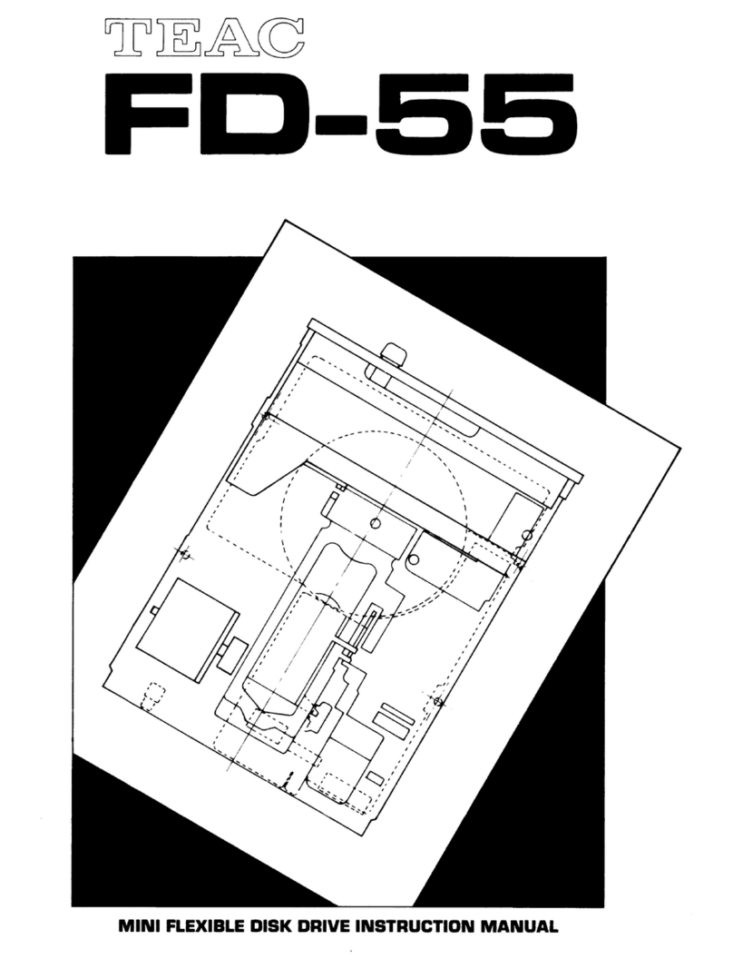
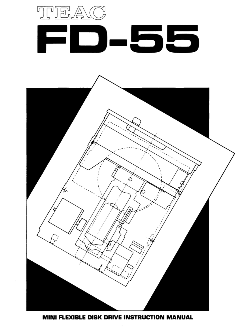
  9. Teac FD-55 Series User manual

Teac FD-55 Series User manual

TEAC.
FD-55 (L)
MINI FLEXIBLE DISK DRIVE
MAINTENANCE MANUAL
ELEKTRONIK
n b n ELEKTRONIK GMBH
Gewerbegebie • 8036 Herrsching
Tel. 081 52/390 • Telex 5 26458
F D -5 5 A F D - 5 5 B F D - 5 5 E F O -5 5 F F D -5 5 G
FM M FM FM M FM FM MFM FM . MFM FM MFM
Trä n st» Rat® K bte/sec) 125 250 125 250 125 250 125 250 250 500
ff
Unformatted Per Track 3.125 6.25 3.125 8.25 3.125 6.25 3.125 6.25 5.208 10.416
Per Disk 125 250 250 500 250 500 500 1.000 302 1.604
Formatted
15 sec-
i tors/irack)
Per Sector 0.128 0.256 0.128 0.256 0.128 0.256 0.128 0.256 -
Per Track 2.048 4 0 9 8 £ 0 45 4.096 2.0 48 4.096 2.048 4.0S6 --
Per Disk 81.32 163.84 163.84 327.58 163.84 327.68 327.36 655.36 - -
Inside Track: Recording Density bpi) 2768 5536 2938 5876 2788 5576 2961 5922 4.935 9.870
Inside Track Flux Density frpi) 5536 5876 5576 5922 9870
Surface !21 2 2
Track Density tpi) 48 96 96
Tracks/Disk 40 80 80 160 160
Track Radius ]
_ mm) |
Outside 57.150 side 57.150 side ? side ?
Inside 36.513 side 36.246 side ? s s ? .. SS?
Average Access Tim e ms) 33 » 94 91
Track Access Time ms) 6 3 3
Settling Time ms) 15 15
n
ELEKTRONIK
nbn ELEKTRONIK GMBH
Gewerbegebieî • 8036 Herrsching
Tel. 08152/390 • 1 ex 05-26458
äfcft -Büro Nord flfe« -Büro West
Tel. 04531/86077 Tel. 021 61/546 77
/
fÄe-Büro Frankfurt
Tel. 06246/7014 ^WI'Böro Stuttgart
Tel. 0711/88 1030 i&ÎMl-Büro Berlin
Tel. 030/8336092 -Büro Nordbayem
Tel.-091 70/8312 fttm -Büro Südbayern
Tel. 081 52/390
hVt>u 2?,, /• « ^ CHIP 237
Title Page
SECTION 3 THEORY OF OPERATION V
...........
.
.............
.
......
.........
300
3-1 CONSTRUCTION AND FUNCTION
...
.
...................
.
.............
.
301 '
3-l-| General Block Diagram
.....
..........
301
3-1-2 Mechanical Section
..
............
302
3-2 CIRCUIT DESCRIPTIONS . . .
.......
.
........
........
.
.............
.
....
307
3-2-1 Read Write Circuit ...
.............
307
3^2-2 Control Circuit
.....
......
.
315
3-2-3 Servo Circuit ..
.......
321
3-3 FONCTION OF TEST POINTS AND VARIABLE RESISTORS
.
.............
.
....
.
322
3-3-1 Function of Test Points
...
.........
323
3-3-2 Function of Variable Resistors
..
...... 330
SECTION 4 MAINTENANCE
.......
. «
.................... .....................
4000
4—1 . GENERAL . . . .
......................
.
........
........................
4001
4-1-1 Periodic Maintenance
.
................
4001
4-1-2 Check and Adjustment
.......
4002
4-1-3 Maintenance Parts Replacement
...............
4004
4-1-4 Maintenance Jigs and Tools
.
.....
.
...........................
.
4 011
4-2 PRECAUTIONS
.........
.
..........
.
.
...........
.
.....................
4014
4-2-1 Torque Applied to Screws and Locking Paint
.
....................
4014
4-2-2 Handling of Connectors
....
4015
4-2-3 Head Cable Treatment
........
4020
4-2-4 Initial Setting of S K A
......
4022
4-2-4-1 Cable connection and setting of power supply voltage ........... 4022
4-2-4-2 Setting of the maximum track number
.
.....................
4025
4-2-4—3 Setting of step rate and settling time
....
.........
4026
4-2~4-4 Level disk calibration .
.
...............
.
..............
.
......
402 8
4-2—4-5 Alignment disk: calibration —
.
.......
.
.......................
.
. 4030
4*2-4-6 Humidity setting
.
..............
.
..........
«
.....
*
..............
4033
4-2-4-7 Setting of SKA gain
.
..................
.
.
........... .
v . 4033
4-2-5 Others
....
4034
4-3 ' PREVENTIVE MAINTENANCE
....
.
................
.
..........
.....
.......
4038
4-3-1 Cleaning of Magnetic Head by Cleaning Disk .
.
.....................
4038
4-3—2 Direct Cleaning (Single sided FDD only)
.........................
4040
4-4 CHECK AND ADJUSTMENT
.
................. ..........
.
..................
4042
4-4-1 Adjustment of Set Arm Position
......
4042
4-4-2 Adjustment of Clamp Arm Position
.
..................
4044
4-4-3 Adjustment of Front Lever Position
...........
4046
4-4-4 Adjustment of Arm Lifter ......................................... 4048
4-4—4-1 Double sided FDD
.....................
4C48
4-4-4-2 Single sided FDD
......
4056
4-4-5 Check of CSS Ass'y ............................................... 4061
4-4-6 Check of File Protect Sensor
....
4065
4-4*7 check and Adjustment of Disk Rotation Speed
..............
4063
4-4*3 check and adjustment of Erase Gate Delay
.......
4071
Title Page
- iii -
4-4-9 Check and Adjustment of Head Touch
.......
.
......
. . .. .
...........
4074
4-4-10 Check and Adjustment of Asymmetry
............
...........
.......
4080
4-4-11 Check of Read Level
.....
......
.
....... . .
.
.......
..........
.....
4085
4-4-12 Check of Resolution
.
...........
.
........
.
..............
.
4089
4-4-13 Check and Adjustment of Track Alignment
.
..............
-
.........
4093
4-4-14 Check and Adjustment of Track 00 Sensor ....C.f..21
.
.............
4102
4-4-15 Check and Adjustment of Track 00 Stopper ...... . . .... . . . .
.......
4109
4-4-16 Check and Adjustment of Index Burst Timing . . .'. . 2. . ...... . . . . 4113
4-5 MAINTENANCE PARTS REPLACEMENT .... .2..Ci
-
.
---
....... 4118
4-5-1 . Replacement of Head Carriage Ass’y
.
.........
4118
4-5-2 Replacement of. Stepping Motor Ass 'y
.
.............
4122
4-5-3 Replacement of DD motor Ass1y (Spindle Motor)
.
...................
4124
4-5-4 Replacement of Collet Ass’y
.
..................
4126
4-5-5 Replacement of Head Load Solenoid
................
4127
4-5-6 Replacement of Track 00 Sensor A ss' y
..............
4129
4-5-7 Replacement of PCBA MFD Control
.............
4130
4-5-8 Replacement of PCBA Front OPT
.
..................... 4132
4-5-9 Replacement of Head Pad (Single sided only) .. —
.
.................
4133
4-5-10 Replacement of Front Bezel Ass1 y
-
-------
-
---------------
........
4135
4-5-11 Replacement of Front Lever Ass'y
.
...............
^ . 4136
4-5-12 Replacement of CSS Ass'y
.
...............
4137
Title Page
iv
SECTION 5 DRAWINGS & PARTS LIST
.......................... ...............
500
5-1 CONFIGURATION
..........
501
5-2 MECHANICAL BREAK-DOWN AND PARTS LIST
....
'........................... 507
5-2-1 FDD
.
.....
.......
.........
.
.......................................
507
5-2-2 Screw, Washer
.
...............
.
...........................
.
........
512
5-3 PCBA PARTS LIST
.....
. •
................
.
............................
513
5-3-1 PCBA MFD Control
....
.
.............
...............................
514
5-3-2 PCBA Front O P T
......
.
........................
....................
520
5-4 SCHEMATIC DIAGRAMS AND PARTS LOCATION
.
..............................
521
Title Page
v -
SECTION 3
THEORY OF OPERATION
300
3-1. CONSTRUCTION AND FUNCTION
3-1-1. General Block Diagram
(Fig.301) General block diagram
301
3-1-2. Mechanical Section
Since the disk is a flexible recording media made of mylar film base
and data interchangeability between disks and FDDs is required, the
mechanical section of the FDD uses precision parts and it is also
assembled with high precision. For this reason, only trained technicians
can handle the internal mechanism. Never apply excessive impact nor
drop the FDD down on the desk.
The mechanical section is constructed’ with frame, door mechanism, disk
clamp mechanism# disk rotation mechanism, magnetic head and carriage,
head load' mechanism (or CSS mechanism) , head seek mechanism, various
detection mechanisms, etc.
(1) Frame «
The main structure for mounting the various mechanisms and printed
circuit boards. The frame is made of aluminum die cast to maintain
the stability of the FDD in strength, precision, durability, and
expansion coefficient.
(2) Door mechanism and disk clamp mechanism
The door mechanism .is constructed with the main parts of set arm which
forms the structure for installing the disk on the spindle other parts
of front*lever, clamp arm, etc. The set arm is sttacKed to the rear
of the frame with leaf springs and on the tip of the set arm a collet,
which forms the disk clamp mechanism, is attached.
When a disk is inserted and the door is closed, the tip of the collet
is inserted in the central window of the disk and the window area is
depressed to the spindle so that the center of the disk is clamped in
the correct position along the outer circumference of the collet.
(3) Disk rotation mechanism
302
The disk rotation mechanism comprises DD motor Ass'y which includes
spindle.
The DD motor is an outor-rotor type DC brushless motor which has the
long life of 30,000 hours or more in continuous rotation.
The rotational speed is 300rpm (or 360rpm) and maintains stable rotat
ional speed against load variations and environmental changes. This is
achieved by a feedback signal from the internal AC tachometer.
The precisely combined collet and spindle are attached at the correct
angle to maintain the center position correctly without damaging the
center hole of the disk and so as to make the head be in contact with
disk at the correct angle.-
(4) Magnetic head and carriage
(Fig.302) External view of magnetic head core
For single sided FDDs, the external view of the magnetic head is button
shaped and it is mounted on the carriage so that it is in contact
with the SIDE 0 (the buttom side when the FDD is placed horizontally)
head window area of the disk.
For double sided FDDs, both the SIDE 1 head and the SIDE 0 head are
special flat type supported with the gimballed mechanisms. The two
magnetic heads are mounted accross the disk on one carriage.
In both types of head, the surface is designed for minimum disk wear
and maximum read output. The head itself is a long life type for
improved head wear. Each head,is constructed with a read/write gap
used for data reading and data writing and two erase gaps to erase the
recorded track edge immediately after the recording (tunnel erase).
The magnetic head and the carriage on which the head is mounted form the
303
(5) Head load mechanism or CSS mechanism
The head load mechanism is used for models with head load solenoid and
the CSS mechanism is used for double sided CSS model without head load
solenoid. Neither of these mechanisms are used for single sided CSS
model.
The head load mechanism functions to make the head in contact with the
disk when only required so as to reduce disk and magnetic head wear.
This mechanism is constructed with head load solenoid , arm lifter, etc.
For a single sided FDD, the head pad attached to the pad arm of the. head
carriage is depressed against the SIDE 1 of the disk with appropriate
pressure and the disk is held with head and head pad. For a double
sided FDD, the SIDE 1 head is depressed with appropriate pressure
instead of the head pad, as well as the single sided FDD.
In the CSS model, the magnetic head is always in contact with a disk
as far as the disk is installed. In order to elongate the disk and
head lives, it is required to make the disk rotate only when it is
necessary. The CSS mechanism (double sided) is constructed with a CSS
Ass * y which is. designed to protect the contact of SIDE 0 and SIDE 1
heads when the front lever is closed if a disk is not installed. For
the purpose of protecting the head beeing cought and damaged by the
head window edge during disk insertion and ejection, the head protector
to lift up the jacket a little is equipped to the CSS Ass'y. The head
protector is also used in the models with head load solenoid.
(6) Head seek mechanism
The head seek mechanism consists mainly of stepping motor with a capstan
(pooly), steel belt (band), guide shafts, and carriage. The carriage
is connected to the capstan of the stepping motor through the steel belt
core section of the FDD and is specially assembled with high precision.
304
and is slided along the guide shafts.
The stepping motor rotates 2 steps (3.6°) for 48tpi and one step (1.8°)
for 96tpi per one track space. To improve the continuity of the
head seek operation and precision of head positioning, hybrid type
4-phase stepping motor is adopted. This special motor is driven in
a unique manner which brought a success in reducing the head ratiation
and to obtain a highly precise positioning.
The parallelism and the distance between the shafts and the center
line of the disk, and shaft and disk themselves are precisely machined.
Also the thermal expansion of the frame, steel belt, carriage, etc. are
taken into consideration in the process of design so that they are
mutually offset with the expansion of the disk.
(7) Detection mechanisms
(a) File protect detection mechanism
This mechanism is constructed with an LED and a photo-transistor to
detect the existence of the write enable notch of the disk jacket.
When a disk with the notch covered is installed and the light pass
for detection is disturbed, no write or erase current will be supplied
to the read/write and erase heads and the recorded information on the
disk is protected from an erroneous input of a write command.
The LED is mounted on the PCBA DD motor servo and the photo-transistor
on the PCBA front OPT.
(b) Track 00 detection mechanism
This mechanism is constructed with a photo-interrupter for detecting
the outermost track position (track 00) of the head and the track 00
stopper which is attached to the rear side of the head carriage.
Inside tracks from the track 00 on the disk are used. Even if an
erroneous step out command is input from the track 00 position, the
command will be ignored by the internal circuit of the FDD.
305
If the head moves out from the track 00 by some reason (such as
impact during transportation), the head carriage strikes the track 00
stopper to protect the head from moving out of the returnable•range
at a next power on.
When step-in commands are input from the innermost track, the head
seeks toward inward and stops with an appropriate space left against
the head window edge of the disk. In order to recalibrate the track
from this position (returning operation to the track 00), it is
required*to input the step-out commands with several additional steps
to the maximum track number.
(c) Index detection mechanism
LED and photo-transistor for the detection of the index hole are
located at the index window area of the disk jacket.
The LED is mounted on the PGBA DD motor servo and the photo-transistor
on the PCBA front OPT. The index hole will be detected along the
rotation of the disk.
306 -
3-2. CIRCUIT DESCRIPTIONS
The electronics of the FDD is constructed with three sections which are
read write circuit, control circuit, and servo circuit. Read write
circuit and control circuit are mounted on the PCBA MFD control, and servo
circuit is .on the PCBA DD motor servo.
3-2-1. Read Write Circuit
The read write circuit is constructed with read circuit, write circuit,
and low voltage sensor. They are mostly packed in a read write LSI
(bipolar).
Fig.303 shows the block diagram.
307
coil Low pas£ Differentiation
filter --- amp.
<
Id
Q
H
tfl H
cn
LVS
SIDE ONE SELECT
Write gate
Erase gate
WRITE DATA
308
(Fig.303) Read write circuit block diagram
(1) Read circuit
The read circuit consists of pre-amplifier, low pass filter, differenti
ation amplifier, peak detector, time domain filter and read gate
(output driver).
In read operation, the minute voltage induced by the read/write head is
amplified about 30dB by the pre-amplifier which.is constructed with a
video band differential amplifier. Undesirable high frequency
noise is eliminated by the low pass filter (L2,L3,C28,etc.) and the
read signal is supplied to the differentiation amplifier (Ql,Q2,Ll,C20,
etc.) . , —
--
----
— .. .
The differentiation amplifier phase-shifts the peak position of fhe
reproduced waveform to the zero cross point, and at the same time,
further amplifies the signal about 20dB with the most appropriate
equalization. The peak detector which is constructed with .a comparator
converts the differentiated output into a square wave.
The time domain filter eliminates a virtual pulse caused by the saddle
in the low frequency area (IF area, 62.5KHz,approx, for models A ^ F ,
and 125KHz for model G) at outer tracks. The time domain filter is
constructed with two edge detectors, 2.4psec, delay single shot (LSI
pin 7, RA9, C23), data latch, and Ipsec data single shot (LSI pins 8
and 9, RA9,C24). -
---
Then the signal is output from the FDD through the read gate, U7 (pins
4 ^ 6 , output driver).
309
Magnetization
on disk
Pre-amp.output
(TP7)
Shoulder
5 V
approx.
Saddle
(Fig.304) Read amp. and peak detector waveforms
310 -
■Virtual pulse (drop-in)
Peak detector
output in U9
Edge detector #1
output in U9
2.4ps delay S.S.
Ç output in U9
if’i
» i
j t.
nn
JLJLJl
2.4ysi approx. n
Data latch output
in U9
Edge detector #2
output in U9
n n r
ti
n
__
_ii
Read data (RD)
(TP5)
(U7,pin 6)
nnnn_
—— 1y s(approx.
U u u"U Ll LT"
(Fig.305) Time domain filter and read gate waveforms
311
(2) Write circuit
The write circuit consists of write power gate (with side selector),
select gate, data latch, write driver, and erase driver.
The write power gate output (COMO or COMl) becomes high voltage when
the write gate signal or the erase gate signal is TRUE (HIGH level).
These signals are generated by the write/erase gate in the control
circuit when all of the following three conditions are satisfied.
(a) The file protect sensor detects the notch of the disk jacket (write
enable condition).
(b) The WRITE GATE input signal is TRUE.
(c) MX strap is on or the DRIVE SELECT signal is TRUE (LOW).
The write power gate output is supplied to the common terminal of the
head through the diode switch. Table 301 shows the output voltage of
the write power gate in various operations,
Conditions Write power gate output voltage
COM 0 (for Side 0) COM 1 (for Side 1)
Side 0 write operation High Low
Side 1 write operation Low High
Side 0 read operation Middle Low
Side 1 read operation Low Middle
High: 10.5V,approx. ' Middle: 4V,approx. Low: 0V,approx.
(Table 301) Write power gate output voltage
The erase gate signal is delayed appropriately against the write gate
signal. Since the erase gap is about 0.85mm (FD-55A ^ F models) or
0.585mm (FD-55G model) behind the read/write gap, it is necessary for
the erase driver to delay the write gate signal so that the written
data is completely trimmed by the erase head (tunnel erase). The
- 312
tunnel erase produces a guard band between the tracks preventing
deterioration of the S/N ratio resulting from a off-track (positioning
error). It also ensures disk interchangeability.
The WRITE DATA input pulse is latched by the data latch. And
appropriate write current is supplied to the read/write bead by turning
on and off the two write drivers alternately. When the write driver is
active, no read data pulse is generated by the read circuit.
WRITE GATE input
Write gate (WG)
(U9,pin 16)
Erase gate (EG)
(TP2)
SIDE ONE SELECT
WRITE DATA irn rir^ in rr^ iriri
Data latch output ru^~u
(Fig.306) Write circuit waveforms
313

Other manuals for FD-55 Series

2

This manual suits for next models

1

Other Teac Floppy Disk Drive manuals

Teac FD-05PUB User manual

Teac

Teac FD-05PUB User manual

Teac FD-235 Series User manual

Teac

Teac FD-235 Series User manual

Teac FD-05PUB User manual

Teac

Teac FD-05PUB User manual

Teac FD-55 Series User manual

Teac

Teac FD-55 Series User manual

Teac FD-55 Series User manual

Teac

Teac FD-55 Series User manual

Teac Internal Floppy Drives User manual

Teac

Teac Internal Floppy Drives User manual

Teac FD-55BR-100 User guide

Teac

Teac FD-55BR-100 User guide

Teac FD-05PU User manual

Teac

Teac FD-05PU User manual

Popular Floppy Disk Drive manuals by other brands

Sony MSFD-20U Specifications

Sony

Sony MSFD-20U Specifications

Fematec 144PRO user manual

Fematec

Fematec 144PRO user manual

Digital Electronics Corporation PL-FD510 installation guide

Digital Electronics Corporation

Digital Electronics Corporation PL-FD510 installation guide

Imation D353FUE Driver Upgrade/Install Information

Imation

Imation D353FUE Driver Upgrade/Install Information

Zenith SM-H-17-4 Service manual

Zenith

Zenith SM-H-17-4 Service manual

Sony MFD-20U operating instructions

Sony

Sony MFD-20U operating instructions

Fujitsu DYNAMO 640SE user guide

Fujitsu

Fujitsu DYNAMO 640SE user guide

Freecom FLOPPY DISK DRIVE datasheet

Freecom

Freecom FLOPPY DISK DRIVE datasheet

Panasonic CF-VFD Series operating instructions

Panasonic

Panasonic CF-VFD Series operating instructions

Sony MPF920-Z User’s Guide Specifications

Sony

Sony MPF920-Z User’s Guide Specifications

manuals.online logo
manuals.online logoBrands
  • About & Mission
  • Contact us
  • Privacy Policy
  • Terms and Conditions

Copyright 2025 Manuals.Online. All Rights Reserved.