Teridian 71M6403 User manual
71M6403
Electronic Trip Unit
SEPTEMBER 2006
Page: 1 of 75 © 2006 TERIDIAN Semiconductor Corporation REV 1.0
GENERAL DESCRIPTION
The Teridian 71M6403 is an electronic trip unit (ETU) system-on-chip
device for air circuit breakers (ACB), molded case circuit breakers
(MCCB) and other types of intelligent switchgear. Utilizing Teridian’s
patented Single Converter Technology, the 71M6403 incorporates a
22-bit delta-sigma ADC, 7 current sensor inputs, digital temperature
compensation, precision voltage reference, 32-bit programmable
computation engine, timers, Real Time Clock (RTC), two UARTs and a
single cycle execution 8-bit MCU.
Armed with an internal digital di/dt integrator, this programmable device
supports either current transformer (CT) or Rogowski-Coils for any or all
input channels and provides instantaneous and delayed over current,
earth-leakage, ground-fault and arc fault protection functions.
Furthermore, the device may be configured to support any number of
conventional or custom protection algorithms that fit specific load
configurations in the field.
The 71M6403 also includes a 5V LCD charge pump as well as 3V LCD
support with up to 168 pixels display and up to 22 DIO pins. Easy
conversion to ROM offers unprecedented cost structure for high volume
MCCB applications.
A complete suite of in-circuit emulator (ICE) and development tools, a
powerful real-time signal monitoring tool, programming libraries and
reference designs enable rapid development of advanced switchgear.
MPU
TIMERS
I0
I1
I2
I3
CK38
CK
VREF
RX
TX
TX
RX
COM0..3
V3.3A V3.3D
V2.5
VBIAS
I4
I5
SEG0..23
DIO 4,5
GNDA GNDD
SEG 24..27
DIO 4..11
SEG 32..41
DIO 12..21
ICE
88.88.8888
Accumulator Indicator
Trip Indicator
External EEPROM
COMPARATOR
Power
Fault
Detection
OPTO
SENSE
DRIVE
SERIAL PORTS
CLOCK
CONVERTER
LCD DRIVER
DIO, PULSE
COMPUTE
ENGINE
FLASH/
ROM
RAM
VOLTAGE REF
REGULATOR
LCD 5V
BOOST
Teridian
71M6403
3/5V LCD
TEMP
SENSOR
19.6608MHz
4040 Counter
Current
Sensors
INEUTRAL
V2
V1
DC in
INEUTRAL
FEATURES
22-bit Sigma-delta converter
Six main sensor inputs
One auxiliary input
Supports CT or Rogowski Coils
Internal di/dt integrators
< 5 msec. startup time
Better than 10ppm/°C accuracy
Instantaneous and delay trip
Peak & RMS current measurement
Calculated or measured GND
current
Power measurement functions
option
Internal temperature sensor
Digital temperature compensation
Independent 32-bit compute engine
Two UART ports
Two timers
Hardware watchdog
Internal power fault detector
Real Time Clock (RTC)
Battery backup (RTC, RAM)
8-bit MPU (80515) - 1 clock cycle
per instruction (5 Mhz max.)
LCD driver ( ≤168 pixels)
5V LCD charge pump
Up to 22 general purpose I/O pins
High speed serial interface (SSI)
I2C EEPROM interface
64KB Flash, 7KB RAM
Flash memory security
30mW @ 3.3V
100-lead LQFP package
Downloaded from Elcodis.com electronic components distributor

71M6403
Electronic Trip Unit
SEPTEMBER 2006
Page: 2 of 75 © 2006 TERIDIAN Semiconductor Corporation REV 1.0
Table of Contents
GENERAL DESCRIPTION .........................................................................................................................1
FEATURES ..................................................................................................................................1
HARDWARE DESCRIPTION .....................................................................................................................8
Hardware Overview ......................................................................................................................8
External Components ...................................................................................................................8
Analog Front End (AFE) ...............................................................................................................8
Multiplexer......................................................................................................................8
ADC ...............................................................................................................................9
FIR Filter ........................................................................................................................9
Voltage Reference .........................................................................................................9
Temperature Sensor ......................................................................................................10
INEUTRAL .....................................................................................................................10
Functional Description....................................................................................................11
Computation Engine (CE).............................................................................................................11
CE Functional Overview.................................................................................................12
Real-Time Monitor..........................................................................................................13
Power Up Short Circuit Detection Time..........................................................................13
80515 MPU Core..........................................................................................................................14
80515 Overview .............................................................................................................14
Memory Organization.....................................................................................................14
Special Function Registers (SFRs) ................................................................................16
Special Function Registers (Generic 80515 SFRs)........................................................17
Special Function Registers Specific to the 71M6403 .....................................................19
Instruction Set ................................................................................................................20
UART .............................................................................................................................21
Timers and Counters......................................................................................................24
WD Timer (Software Watchdog Timer) ..........................................................................27
Interrupts........................................................................................................................29
External Interrupts..........................................................................................................32
Interrupt Priority Level Structure.....................................................................................33
Interrupt Sources and Vectors........................................................................................34
Downloaded from Elcodis.com electronic components distributor

71M6403
Electronic Trip Unit
SEPTEMBER 2006
Page: 3 of 75 © 2006 TERIDIAN Semiconductor Corporation REV 1.0
On-Chip Resources ......................................................................................................................35
DIO Ports .......................................................................................................................35
Physical Memory............................................................................................................36
Real-Time Clock (RTC)..................................................................................................37
Comparators (V2, INEUTRAL) .......................................................................................38
LCD Drivers....................................................................................................................38
LCD Voltage Boost Circuitry...........................................................................................38
UART (UART0) and Optical Port (UART1) ....................................................................39
Hardware Reset Mechanisms ........................................................................................39
Reset Pin (RESETZ) ......................................................................................................39
Hardware Watchdog Timer ............................................................................................39
Internal Voltages (VBIAS and V2P5)..............................................................................40
Internal Clocks and Clock Dividers.................................................................................41
I2C Interface (EEPROM) ................................................................................................41
Test Ports.......................................................................................................................42
FUNCTIONAL DESCRIPTION ...................................................................................................................44
System Timing Summary .............................................................................................................44
Data Flow .....................................................................................................................................46
CE/MPU Communication..............................................................................................................46
Fault, Reset, Power-Up ................................................................................................................48
Chopping Circuitry ........................................................................................................................48
Program Security..........................................................................................................................49
FIRMWARE INTERFACE...........................................................................................................................50
I/O RAM MAP – In Numerical Order.............................................................................................50
SFR MAP (SFRs Specific to TERIDIAN 80515) – In Numerical Order .........................................51
I/O RAM (Configuration RAM) – Alphabetical Order.....................................................................52
CE Program and Environment......................................................................................................58
CE Program ...................................................................................................................58
Formats..........................................................................................................................58
Constants.......................................................................................................................58
Environment ...................................................................................................................58
CE Calculations..............................................................................................................59
CE RAM Locations .......................................................................................................................59
CE Front End Data (Raw Data)......................................................................................59
Input Configuration.........................................................................................................60
Accumulation Strobe Output ..........................................................................................60
Downloaded from Elcodis.com electronic components distributor

71M6403
Electronic Trip Unit
SEPTEMBER 2006
Page: 4 of 75 © 2006 TERIDIAN Semiconductor Corporation REV 1.0
Processed Current Data.................................................................................................61
Overcurrent Detection ....................................................................................................61
MPU Firmware Library..................................................................................................................63
SPECIFICATIONS......................................................................................................................................64
Electrical Specifications................................................................................................................64
ABSOLUTE MAXIMUM RATINGS.................................................................................64
RECOMMENDED OPERATING CONDITIONS.............................................................65
LOGIC LEVELS .............................................................................................................65
SUPPLY CURRENT ......................................................................................................66
2.5V VOLTAGE REGULATOR ......................................................................................66
VREF, VBIAS.................................................................................................................67
ADC CONVERTER, VDD REFERENCED .....................................................................68
OPTICAL INTERFACE ..................................................................................................68
TEMPERATURE SENSOR............................................................................................68
LCD BOOST ..................................................................................................................69
LCD DRIVERS ...............................................................................................................69
RESETZ.........................................................................................................................69
COMPARATORS ...........................................................................................................69
RAM AND FLASH MEMORY.........................................................................................70
FLASH MEMORY TIMING.............................................................................................70
EEPROM INTERFACE ..................................................................................................70
Packaging Information..................................................................................................................71
Pinout (Top View)...........................................................................................................72
Pin Descriptions .............................................................................................................73
ORDERING INFORMATION ........................................................................................................75
Downloaded from Elcodis.com electronic components distributor

71M6403
Electronic Trip Unit
SEPTEMBER 2006
Page: 5 of 75 © 2006 TERIDIAN Semiconductor Corporation REV 1.0
Figures
Figure 1: IC Functional Block Diagram................................................................................................................................7
Figure 2: General Topology of a Chopped Amplifier..........................................................................................................10
Figure 3: AFE Block Diagram ............................................................................................................................................11
Figure 4: Samples in Multiplexer Cycle .............................................................................................................................12
Figure 5: Memory Map .....................................................................................................................................................14
Figure 6: DIO Ports Block Diagram...................................................................................................................................35
Figure 7: LCD Voltage Boost Circuitry...............................................................................................................................39
Figure 8: V1 Input Voltage Thresholds..............................................................................................................................40
Figure 9: Timing Relationship between ADC MUX, CE, and Serial Transfers .....................................................................44
Figure 10: RTM Output Format.........................................................................................................................................45
Figure 11: SSI Timing, (SSI_FPOL = SSI_RDYPOL = 0) ................................................................................................... 45
Figure 12: SSI Timing, 16-bit Field Example (External Device Delays SRDY)....................................................................45
Figure 13: MPU/CE Data Flow...........................................................................................................................................46
Figure 14: MPU/CE Communication (Functional)..............................................................................................................47
Figure 15: MPU/CE Communication (Processing Sequence) ............................................................................................47
Figure 16: Chop Polarity w/ Automatic Chopping..............................................................................................................48
Tables
Table 1: Inputs Selected in Regular and Alternate Multiplexer Cycles (EQU = 5).................................................................8
Table 2: CE DRAM Locations for ADC Results..................................................................................................................12
Table 3: Stretch Memory Cycle Width...............................................................................................................................15
Table 4: Internal Data Memory Map..................................................................................................................................16
Table 5: Special Function Registers Locations..................................................................................................................16
Table 6: Special Function Registers Reset Values.............................................................................................................17
Table 7: PSW Register Flags.............................................................................................................................................18
Table 8: PSW bit functions ...............................................................................................................................................18
Table 9: Port Registers.....................................................................................................................................................19
Table 10: Special Function Registers ................................................................................................................................20
Table 11: Baud Rate Generation .......................................................................................................................................21
Table 12: UART Modes.....................................................................................................................................................21
Table 13: The S0CON Register .........................................................................................................................................22
Table 14: The S1CON register...........................................................................................................................................22
Table 15: The S0CON Bit Functions ..................................................................................................................................22
Table 16: The S1CON Bit Functions ..................................................................................................................................23
Table 17: The TMOD Register...........................................................................................................................................24
Table 18: TMOD Register Bit Description..........................................................................................................................24
Table 19: Timers/Counters Mode Description...................................................................................................................25
Table 20: The TCON Register............................................................................................................................................ 25
Table 21: The TCON Register Bit Functions ......................................................................................................................25
Table 22: Timer Modes..................................................................................................................................................... 26
Downloaded from Elcodis.com electronic components distributor

71M6403
Electronic Trip Unit
SEPTEMBER 2006
Page: 6 of 75 © 2006 TERIDIAN Semiconductor Corporation REV 1.0
Table 23: The PCON Register ...........................................................................................................................................26
Table 24: PCON Register Bit Description ..........................................................................................................................26
Table 25: The IEN0 Register .............................................................................................................................................27
Table 26: The IEN0 Bit Functions...................................................................................................................................... 27
Table 27: The IEN1 Register .............................................................................................................................................27
Table 28: The IEN1 Bit Functions...................................................................................................................................... 27
Table 29: The IP0 Register ...............................................................................................................................................28
Table 30: The IP0 bit Functions ........................................................................................................................................28
Table 31: The WDTREL Register.......................................................................................................................................28
Table 32: The WDTREL Bit Functions ...............................................................................................................................28
Table 33: The IEN0 Register .............................................................................................................................................29
Table 34: The IEN0 Bit Functions...................................................................................................................................... 29
Table 35: The IEN1 Register .............................................................................................................................................30
Table 36: The IEN1 Bit Functions...................................................................................................................................... 30
Table 37: The IEN2 Register .............................................................................................................................................30
Table 38: The IEN2 Bit Functions...................................................................................................................................... 30
Table 39: The TCON Register............................................................................................................................................ 31
Table 40: The TCON Bit Functions .................................................................................................................................... 31
Table 41: The IRCON Register ..........................................................................................................................................31
Table 42: The IRCON Bit Functions...................................................................................................................................31
Table 43: External MPU Interrupts....................................................................................................................................32
Table 44: Control Bits for External Interrupts....................................................................................................................32
Table 45: Priority Level Groups ........................................................................................................................................33
Table 46: The IP0 Register: .............................................................................................................................................. 33
Table 47: The IP1 Register: .............................................................................................................................................. 33
Table 48: Priority Levels ...................................................................................................................................................33
Table 49: Interrupt Polling Sequence................................................................................................................................34
Table 50: Interrupt Vectors...............................................................................................................................................34
Table 51: Direction Registers and Internal Resources for DIO Pin Groups........................................................................35
Table 52: DIO_DIR Control Bit..........................................................................................................................................35
Table 53: Selectable Controls using the DIO_DIR Bits ......................................................................................................36
Table 54: MPU Data Memory Map.................................................................................................................................... 36
Table 55: Liquid Crystal Display Segment Table (Typical).................................................................................................38
Table 56: EECTRL Status Bits...........................................................................................................................................41
Table 57: TMUX[3:0] Selections .......................................................................................................................................42
Table 58: SSI Pin Assignment ..........................................................................................................................................43
Table 59: CHOP_EN Bits...................................................................................................................................................48
Downloaded from Elcodis.com electronic components distributor
71M6403
Electronic Trip Unit
SEPTEMBER 2006
Page: 7 of 75 © 2006 TERIDIAN Semiconductor Corporation REV 1.0
I0
I1
I2
I3
MUX
CK38
CK
VREF
CKTEST
CE
32-bit Compute
Engine
MPU
(80515)
CE
CONTROL
OPT_RX
OPT_TX
RESETZ
V1 EMULATOR
PORT
CE_BUSY
OPTICAL
I/F
UART
TX
RX
XFER BUSY
CE PROG
RAM
(4KB)
COM0..3
LCD DISPLAY
DRIVER
RTC
DATA
00-FF
PROG
000-7FF
DATA
0000-FFFF
PROG
0000-FFFF
MPU XRAM
(2KB)
0000-07FF
DIGITAL I/O
CONFIG
RAM
(I/O RAM)
2000-20FF
I/O RAM
CE DATA
RAM
(1KB)
MEMORY
SHARE
3000-3FFF
1000-13FF
RTCLK
MUX_SYNC
CKCE
CKMPU
V2
CE_RUN
CE_LOAD
CE_EN
RTM_EN
COMP_INT
COMP_STAT
WATCHDOG
POWER FAULT
GENERATOR AND
COMPARATORS
LCD_CLK
LCD_MODE
DIO_GP
RTC_SET
4.9MHz
4.9MHz
GNDD
V3P3A
V3P3D
VBAT
VOLT
REG
2.5V to logic V2P5
MPU_DIV
SUM_CYCLES
PRE_SAMPS
CKOUT_EN VLCD
TMUXOUT
FAULTZ
WAKE
VBIAS
DMUX
TMUX
CONFIGURATION
PARAMETERS
VDRV
GNDA
I4
TEMP
September 9, 2006
CK_GEN
CK32
CK_EN
CLK
divider
VOLTAGE
BOOST
LCD_BSTEN
LCD_IBST
VREF
VREF_DIS
MUX
CTRL
MUX_DIV
CHOP_EN
STRT
I5
MUX
CKFIR
4.9MHz
MUX_SYNC
RTM
RTM
SEG20..23
DIO_0..3
SEG28/DIO8 ..
SEG31/DIO11
GNDA
GNDD
FAULT_PULSE
STROBE
FAULT_PULSE
STROBE
TEST3
LCD_FS
LCD_MODE
LCD_EN
GNDD
LCD_NUM
DIO_OUT
DIO_IN
LCD_NUM
RTC_HOLD
0
1
2
3
4
5
6
7
8
9
A
B
C
D
E
F
DGND
IBIAS
WDTR_EN
V2 OK
V3 OK
OPTRX
ANALOG
DIGITAL
STROBE
MUX_ALT
SEG24/DIO4 ..
SEG27/DIO7
SEG32/DIO12 ..
SEG41/DIO21
SCL
SDA
FLASH
(64KB)
EEWRSLOW
EERDSLOW
V3P3A
FIR_LEN
FIR
FILTER
CK_10M
CK_MPU
reserved
SEG0..2, SEG3/SCLK,
SEG4/SSDATA,
SEG5/SFR, SEG7..19
EEPROM
INTERFACE
DIO_EEX
PLL_2.5V
ECK_DIS
OPT_TXDIS
GNDD
∆Σ ADC
CONVERTER
+
-
VREF
RTCLK
CE_BUSY
XFER_BUSY
VBIAS
V3P3
V2P5
SEG6/SRDY
VBIAS
VBIAS
PLLOUT
SSI
INEUTRA
L
INEUTRAL
38kHz
19.66MH
z
FAULT_PULSE
Figure 1: IC Functional Block Diagram
Downloaded from Elcodis.com electronic components distributor
71M6403
Electronic Trip Unit
SEPTEMBER 2006
Page: 8 of 75 © 2006 TERIDIAN Semiconductor Corporation REV 1.0
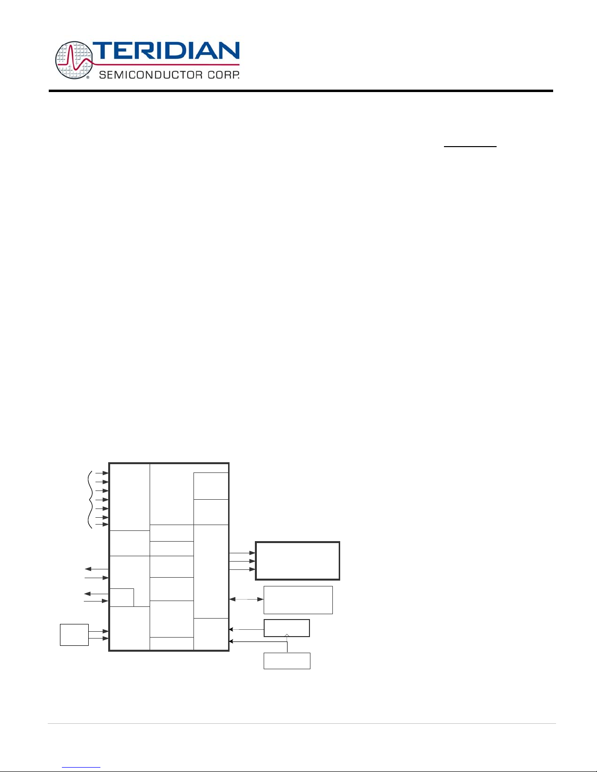
HARDWARE DESCRIPTION
Hardware Overview
The TERIDIAN 71M6403 single chip Electronic Trip Unit integrates all primary functional blocks required to implement a solid-
state circuit breaker. Included on chip are an analog front end (AFE), an 8051-compatible microprocessor (MPU) which executes
one instruction per clock cycle (80515), an independent 32-bit digital computation engine (CE), a voltage reference, LCD drivers,
RAM, FLASH memory, and a variety of I/O pins. Various current sensor technologies are supported including Current
Transformers (CT), Resistive Shunts, and Rogowski (di/dt) Coils.
Measurements can be displayed on either a 3V or a 5V LCD. Flexible mapping of LCD display segments will facilitate integration
with any LCD format. The design trade-off between the number of LCD segments and DIO pins can be flexibly configured using
memory-mapped I/O to accommodate various requirements.
The 71M6403 includes several I/O peripheral functions that improve the functionality of the device and reduce the component
count for most circuit breaker applications. The I/O peripherals include two UARTs, digital I/O, comparator inputs, LCD display
drivers, I2C interface and an optical/IR interface.
One of the two internal UARTs (UART1) is adapted to support an Infrared LED with higher internal drive output and sense input.
It can also be configured to function as a standard UART with normal digital IOs.
A block diagram of the chip is shown in Figure 1. A detailed description of various hardware blocks follows.
External Components
The 71M6403 is optimized for fast startup. To achieve this, an external 19.6608 MHz oscillator is required to drive CK, the
primary clock input. The frequency for the CK38 input is generated from the 19.6608 MHz oscillator using an inexpensive
‘HC4040 counter chip. The divide-by-512 output of the ‘HC4040 generates a 38.4 kHz signal.
Analog Front End (AFE)
The AFE of the TERIDIAN 71M6403 Electronic Trip Unit IC is comprised of an input multiplexer, a delta-sigma A/D converter
with internal voltage reference, followed by an FIR filter. A block diagram of the AFE is shown in Figure 3.
Multiplexer
The input multiplexer supports eight input signals that are applied to the pins I0 through I5, INEUTRAL plus the output of the
internal temperature sensor. The multiplexer can be operated in two modes:
• During a normal multiplexer cycle, the signals from the six pins I0 through I5 are selected.
• During the alternate multiplexer cycle, the temperature signal (TEMP) , INEUTRAL, and I1, I3, I4, I5 (EQU = 101) signal
sources are selected. Use of the alternate multiplexer cycle is not recommended for fast response circuit breaker
applications. Upon enabling the alternate multiplexer cycle, the I0 and I2 current samples are interrupted delaying over
current trip detection response time.
Regular multiplexer sequence
Mux State:
Alternate multiplexer sequence
Mux State:
0 1 2 3 4 5 0 1 2 3 4 5
I0 I1 I2 I3 I4 I5 TEMP I1 INEUTRAL I3 I4 I5
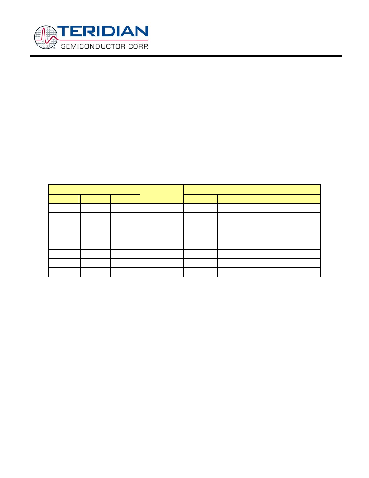
Table 1: Inputs Selected in Regular and Alternate Multiplexer Cycles (EQU = 101)
Note: Use of the alternate multiplexer cycle is not recommend.
Downloaded from Elcodis.com electronic components distributor

71M6403
Electronic Trip Unit
SEPTEMBER 2006
Page: 9 of 75 © 2006 TERIDIAN Semiconductor Corporation REV 1.0
In a typical application, the I0 through I5 inputs are connected to current transformers or Rogowski coils that sense the current
on each phase of the line voltage.
The Multiplexer Control Circuit handles the setting of the multiplexer. The function of the Multiplexer Control Circuit is governed
by the I/O RAM registers MUX_ALT (0x2005[2]) and MUX_DIV (0x2002[7:6]). MUX_DIV controls the number of samples per
cycle. It can request 2, 3, 4, or 6 multiplexer states per cycle.
Multiplexer Control Circuit also controls the FIR filter initiation and the chopping of the ADC reference voltage, VREF. The
Multiplexer Control Circuit is clocked by PLLOUT, the 32768Hz clock from the PLL block derived from CK, and launches each
pass through the CE program.
ADC
A single 21/22-bit delta-sigma A/D converter digitizes the power inputs to the AFE. The ADC inputs I0 - I5 are referenced to
V3P3A with an input voltage range of ± 250 mv. The resolution of the ADC is programmable using the I/O RAM register
FIR_LEN register (0x2005[4]). ADC resolution may be selected to be 21 bits (FIR_LEN=0), or 22 bits (FIR_LEN=1). Conversion
time is two cycles of PLLOUT with FIR_LEN = 0 and three cycles with FIR_LEN = 1.
Accuracy, timing and functional specifications in this data sheet are based on FIR_LEN = 0 (two PLLOUT cycles).
Initiation of each ADC conversion is controlled by the Multiplexer Control Circuit as described previously.
FIR Filter
The finite impulse response (FIR) filter is an integral part of the ADC and it is optimized for use with the multiplexer. The purpose
of the FIR is to decimate the ADC output to the desired resolution. At the end of each ADC conversion, the output data of the
FIR filter (raw data) is stored into the CE Data RAM (DRAM) location determined by the multiplexer selection. The location of the
raw data in the CE DRAM is specified in the CE Program and Environment Section.
Voltage Reference
The 71M6403 includes an on-chip precision bandgap voltage reference that incorporates auto-zero techniques. The reference of
the 71M6403 is trimmed in production to minimize errors caused by component mismatch and drift. The result is a voltage output
with a predictable temperature coefficient.
The voltage reference is chopper stabilized, i.e. the polarity can be switched by the MPU using the I/O RAM register CHOP_ENA
(0x2002[5:4]). The two bits in the CHOP_ENA register enable the MPU to operate the chopper circuit in regular or inverted
operation, or in “toggling” mode. When the chopper circuit is toggled in between multiplexer cycles, DC offsets on the measured
signals will automatically be averaged out.
Downloaded from Elcodis.com electronic components distributor
71M6403
Electronic Trip Unit
SEPTEMBER 2006
Page: 10 of 75 © 2006 TERIDIAN Semiconductor Corporation REV 1.0
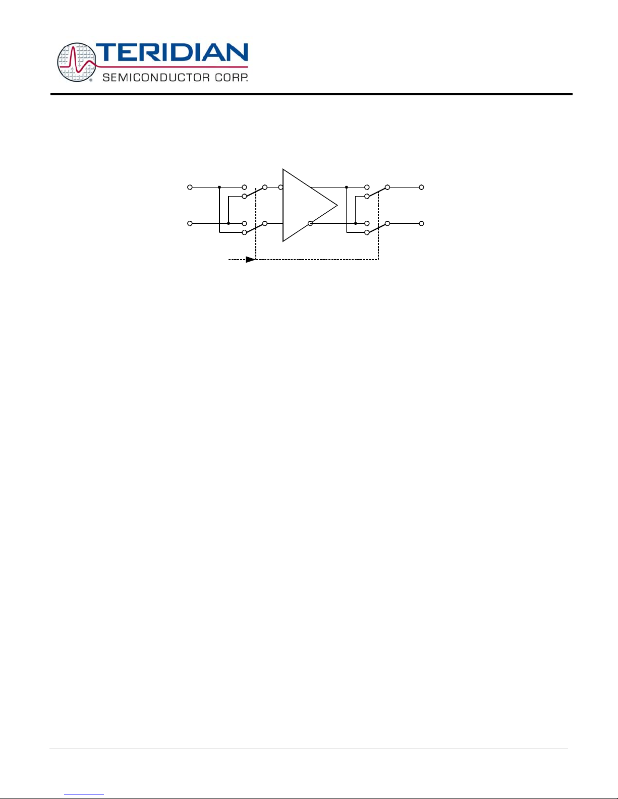
The general topology of a chopped amplifier is given in Figure 2.
G
-
+V
inp
V
outp
V
outn
V
inn
CROSS
A
B
A
B
A
B
A
B
Figure 2: General Topology of a Chopped Amplifier
It is assumed that an offset voltage Voff appears at the positive amplifier input. With all switches, as controlled by CROSS in the
“A” position, the output voltage is:
Voutp – Voutn = G (Vinp + Voff – Vinn) = G (Vinp – Vinn) + G Voff
With all switches set to the “B” position by applying the inverted CROSS signal, the output voltage is:
Voutn – Voutp = G (Vinn – Vinp + Voff) = G (Vinn – Vinp) + G Voff, or
Voutp – Voutn = G (Vinp – Vinn) - G Voff
Thus, when CROSS is toggled, e.g. after each multiplexer cycle, the offset will alternately appear on the output as positive and
negative, which results in the offset effectively being eliminated, regardless of its polarity or magnitude.
The Functional Description Section contains a chapter with a detailed description on controlling the CHOP_ENA register.
Temperature Sensor
The 71M6403 includes an on-chip temperature sensor implemented as a bandgap reference. It is used to determine the die
temperature. The MPU may request an alternate multiplexer cycle containing the temperature sensor output by asserting
MUX_ALT.
Reading the internal temperature sensor requires enabling the alternate multiplexer cycle. The alternate multiplexer cycle then
displaces a normal I0-I5 current sensors acquisition cycle. Therefore, detection of an over current event may be delayed.
INEUTRAL
INEUTRAL is an analog monitor input that can be used for additional analog measurements, such as neutral current. It is
sampled when the multiplexer performs an alternate multiplexer cycle. The zero reference for the INEUTRAL input is VBIAS.
INEUTRAL is also routed into the comparator block where it is compared to VBIAS. External interrupt 2 should be disabled when
the INEUTRAL input is used for analog measurements.
Downloaded from Elcodis.com electronic components distributor

71M6403
Electronic Trip Unit
SEPTEMBER 2006
Page: 11 of 75 © 2006 TERIDIAN Semiconductor Corporation REV 1.0
Functional Description
The AFE functions as a data acquisition system, controlled by the MPU. The main signals (I0, I3, I1, I4, I2, I5) are sampled and
the ADC counts obtained are stored in CE RAM where they can be accessed by the CE and, if necessary, by the MPU.
I0
I1
I2
I3
MUX
VREF VBIAS
I4
TEMP
CK32
VREF
VREF_DIS
MUX
CTRL
MUX_DIV
CHOP_EN
I5
MUX_ALT
V3P3A
FIR_LEN
FIR
FILTER
∆Σ ADC
CONVERTER
+
-
VREF
VBIAS
INEUTRAL
Figure 3: AFE Block Diagram
Computation Engine (CE)
The CE, a dedicated 32-bit RISC processor, performs the precision computations necessary to accurately measure currents.
The CE calculations and processes include:
• Scaling of the processed samples based on chip temperature (temperature compensation) and calibration coefficients.
The CE program RAM (CE PRAM) is loaded at boot time by the MPU and then executed by the CE. Each CE instruction word is
2 bytes long. The CE program counter begins a pass through the CE code each time multiplexer state 0 begins. The code pass
ends when a HALT instruction is executed. For proper operation, the code pass must be completed before the multiplexer cycle
ends (see System Timing Summary in the Functional Description Section).
The CE data RAM (CE DRAM) is shared by the FIR filter block, the RTM circuit, the CE, and the MPU. Assigned time slots are
reserved for FIR, RTM, and MPU, respectively, such that memory accesses to CE_RAM do not collide. Holding registers are
used to convert 8-bit wide MPU data to/from 32-bit wide CE DRAM data, and wait states are inserted as needed, depending on
the frequency of CKMPU.
Table 2 shows the CE DRAM addresses allocated to analog inputs from the AFE.
Downloaded from Elcodis.com electronic components distributor

71M6403
Electronic Trip Unit
SEPTEMBER 2006
Page: 12 of 75 © 2006 TERIDIAN Semiconductor Corporation REV 1.0
Address Name Zero
Reference Description
0x00 I0 V3P3 Current input 0
0x01 I1 V3P3 Current input 1
0x02 I2 V3P3 Current input 2
0x03 I3 V3P3 Current input 3
0x04 I4 V3P3 Current input 4
0x05 I5 V3P3 Current input 5
0x06 TEMP --- Temperature
0x07 INEUTRAL VBIAS INEUTRAL
monitor
Table 2: CE DRAM Locations for ADC Results
CE Functional Overview
The ADC processes one sample per channel per multiplexer cycle. Figure 4 shows the timing of the six samples taken during
one multiplexer cycle.
The ADC sampling process and resultant accumulation interval calculations are described in the CE Program section.
I1
I3
I2
I5
I4
I0
1/2520.6Hz = 397µs
2/32768Hz =
61.04µs
13/32768Hz = 397µs
per mux cycle
I1
I3
I2
I5
I4
I0
1/2520.6Hz = 397µs
2/32768Hz =
61.04µs
13/32768Hz = 397µs
per mux cycle
Figure 4: Samples in Multiplexer Cycle
Downloaded from Elcodis.com electronic components distributor
71M6403
Electronic Trip Unit
SEPTEMBER 2006
Page: 13 of 75 © 2006 TERIDIAN Semiconductor Corporation REV 1.0
Real-Time Monitor
The CE contains a Real Time Monitor (RTM), which can be programmed to monitor four selectable CE RAM locations at full
sample rate. The four monitored locations are serially output to the TMUXOUT pin via the digital output multiplexer at the
beginning of each CE code pass (see the Test Ports Section for details)
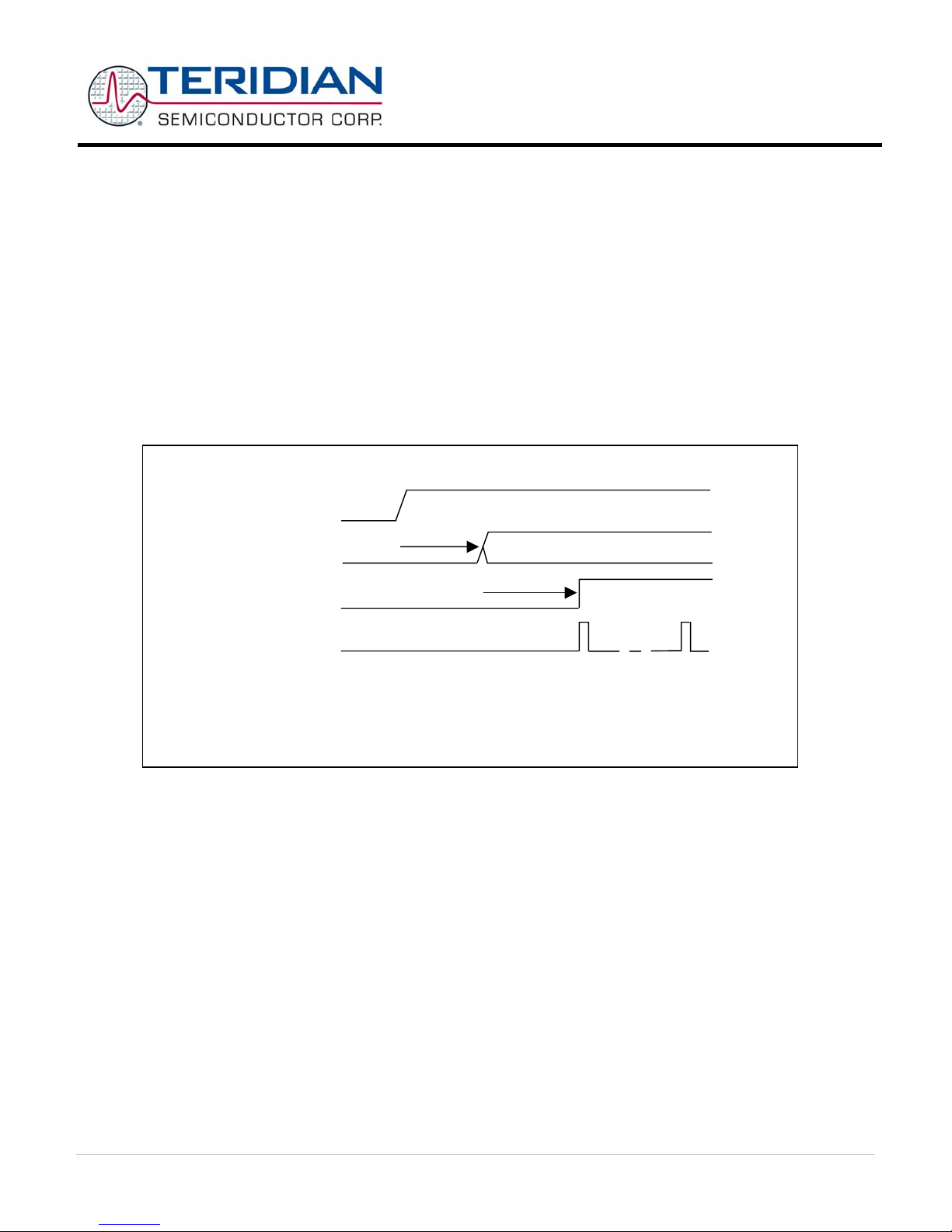
Power Up Short Circuit Detection Time
The 71M6403 detects a short circuit condition within less than 5 msec. (T2) after application of its power and a stable reference
clock. This delay includes the firmware startup time for both the CE and the MPU, and for the CE to complete its initial
measurements. The following diagram shows the timing delay of a CE trip indication relative to application of power and the
reference clock.
Power Up Detection Time
The T1 delay is a system parameter dependent on the system clock architecture. T1 could be the start up time for an external
oscillator powered from the same power source as the 71M6403, or T1 could be the delay from a system wide reference clock.
If the reference clock is already stable prior to application of power to the 71M6403 (using a system wide reference clock), the
T1 delay is eliminated. The resultant start up delay reduces to T2 assuming a “clean” application of power to the 71M6403.
71M6403 Powe
r
Reference Clock
CE FAULT_PULSE
CE STROBE
T1
T2
T1: Delay to stable reference clock operation
T2: Delay to CE FAULT_PULSE assertion and
first CE STROBE pulse ( < 5 msec)
Downloaded from Elcodis.com electronic components distributor

71M6403
Electronic Trip Unit
SEPTEMBER 2006
Page: 14 of 75 © 2006 TERIDIAN Semiconductor Corporation REV 1.0
80515 MPU Core
80515 Overview
The 71M6403 includes an 80515 MPU (8-bit, 8051-compatible) that processes most instructions in one clock cycle. Using a
5MHz clock results in a processing throughput of 5 MIPS. The 80515 architecture eliminates redundant bus states and im-
plements parallel execution of fetch and execution phases. Normally a machine cycle is aligned with a memory fetch, therefore,
most of the 1-byte instructions are performed in a single cycle. This leads to an 8x performance (in average) improvement (in
terms of MIPS) over the Intel 8051 device running at the same clock frequency.
Actual processor clocking speed can be adjusted to the total processing demand of the application (current and trip calculations,
memory management, LCD driver management and I/O management) using the I/O RAM register MPU_DIV[2:0].
Typical measurement and circuit breaker functions based on the internal 32-bit compute engine (CE) results are available for the
MPU as part of TERIDIAN’s standard library. A standard ANSI “C” 80515-application programming interface library is available
to help reduce design cycle time.
Memory Organization
The 80515 MPU core incorporates the Harvard architecture with separate code and data spaces.
Memory organization in the 80515 is similar to that of the industry standard 8051. There are three memory areas: Program
memory (Flash), external data memory (physically consisting of XRAM, CE Data RAM, CE Program RAM and I/O RAM), and
internal data memory (Internal RAM). Figure 5 shows the memory map (see also Table 54).
Internal and External Data Memory: Both internal and external data memory are physically located in the 71M6403 IC. Ex-
ternal data memory is only meant to imply external to the 80515 MPU core.
0xFFFF 0xFFFF
0x4000 ---
0x3FFF
0x3000 CE PRAM
0x2FFF
0x2100 ---
0x20FF
0x2000 I/O RAM
0x1FFF
0x1400 ---
0x13FF
0x1000 CE DRAM
0x0FFF
0x0800 ---
0x07FF 0xFF
0x0000
Flash memory
0x0000 XRAM 0x00
SFRs, RAM,
reg. banks
Program memory External data memory Internal data memory
Figure 5: Memory Map
Program Memory: The 80515 can address up to 64KB of program memory space from 0x0000 to 0xFFFF. Program memory is
read when the MPU fetches instructions or performs a MOVC operation.
After reset, the MPU starts program execution from location 0x0000. The lower part of the program memory includes reset and
interrupt vectors. The interrupt vectors are spaced at 8-byte intervals, starting from 0x0003.
Downloaded from Elcodis.com electronic components distributor
71M6403
Electronic Trip Unit
SEPTEMBER 2006
Page: 15 of 75 © 2006 TERIDIAN Semiconductor Corporation REV 1.0
External Data Memory: While the 80515 can address up to 64KB of external data memory in the space from 0x0000 to
0xFFFF, only the memory ranges shown in Figure 5 contain physical memory. The 80515 writes into external data memory when
the MPU executes a MOVX @Ri,A or MOVX @DPTR,A instruction. The MPU reads external data memory by executing a
MOVX A,@Ri or MOVX A,@DPTR instruction (SFR USR2 provides the upper 8 bytes for the MOVX A,@Ri instruction).
Clock Stretching: MOVX instructions can access fast or slow external RAM and external peripherals. The three low ordered
bits of the CKCON register define the stretch memory cycles. Setting all the CKCON stretch bits to one allows access to very
slow external RAM or external peripherals.
Table 3 shows how the signals of the External Memory Interface change when stretch values are set from 0 to 7. The widths of
the signals are counted in MPU clock cycles. The post-reset state (001) of the CKCON register, which is in bold in the table,
performs the MOVX instructions with a stretch value equal to 1.
CKCON register Read signals width Write signal width
CKCON.2 CKCON.1 CKCON.0
Stretch Value
memaddr memrd memaddr memwr
0 0 0 0 1 1 2 1
0 0 1 1 2 2 3 1
0 1 0 2 3 3 4 2
0 1 1 3 4 4 5 3
1 0 0 4 5 5 6 4
1 0 1 5 6 6 7 5
1 1 0 6 7 7 8 6
1 1 1 7 8 8 9 7
Table 3: Stretch Memory Cycle Width
Direct vs Paged Addressing: There are two types of instructions, differing in whether they provide an eight-bit or sixteen-bit
indirect address to the external data RAM.
In the first type (MOVX A,@Ri), the contents of R0 or R1, in the current register bank, provide the eight lower-ordered bits of
address. The eight high-ordered bits of address are specified with the USR2 SFR. This method allows the user paged access
(256 pages of 256 bytes each) to the full 64KB of external data RAM. In the second type of MOVX instruction (MOVX
A,@DPTR), the data pointer generates a sixteen-bit address. This form is faster and more efficient when accessing very large
data arrays (up to 64 Kbytes), since no additional instructions are needed to set up the eight high ordered bits of address.
It is possible to mix the two MOVX types. This provides the user with four separate data pointers, two with direct access and two
with paged access to the entire 64KB of external memory range.
Dual Data Pointer: The Dual Data Pointer accelerates the block moves of data. The standard DPTR is a 16-bit register that is
used to address external memory or peripherals. In the 80515 core, the standard data pointer is called DPTR, the second data
pointer is called DPTR1. The data pointer select bit chooses the active pointer. The data pointer select bit is located at the LSB
of the DPS register (DPS.0). DPTR is selected when DPS.0 = 0 and DPTR1 is selected when DPS.0 = 1.
The user switches between pointers by toggling the LSB of the DPS register. All DPTR-related instructions use the currently
selected DPTR for any activity.
The second data pointer may not be supported by certain compilers.
Downloaded from Elcodis.com electronic components distributor

71M6403
Electronic Trip Unit
SEPTEMBER 2006
Page: 16 of 75 © 2006 TERIDIAN Semiconductor Corporation REV 1.0
Internal Data Memory: The Internal data memory provides 256 bytes (0x00 to 0xFF) of data memory. The internal data memory
address is always 1 byte wide and can be accessed by either direct or indirect addressing. The Special Function Registers
occupy the upper 128 bytes. This SFR area is available only by direct addressing. Indirect addressing accesses the upper
128 bytes of Internal RAM.
The lower 128 bytes contain working registers and bit-addressable memory. The lower 32 bytes form four banks of eight
registers (R0-R7). Two bits on the program memory status word (PSW) select which bank is in use. The next 16 bytes form a
block of bit-addressable memory space at bit addressees 0x00-0x7F. All of the bytes in the lower 128 bytes are accessible
through direct or indirect addressing. Table 4 shows the internal data memory map.
Address Direct addressing Indirect addressing
0xFF
0x80
Special Function Registers
(SFRs) RAM
0x7F
0x30 Byte-addressable area
0x2F
0x20 Bit-addressable area
0x1F
0x00 Register banks R0…R7
Table 4: Internal Data Memory Map
Special Function Registers (SFRs)
A map of the Special Function Registers is shown in Table 5.
Hex\Bin X000 X001 X010 X011 X100 X101 X110 X111 Bin/Hex
F8 INTBITS
FF
F0 B
F7
E8 WDI
EF
E0 A
E7
D8 WDCON DF
D0 PSW D7
C8
CF
C0 IRCON C7
B8 IEN1 IP1 S0RELH S1RELH USR2
BF
B0
FLSHCTL
PGADR B7
A8 IEN0 IP0 S0RELL AF
A0 P2 DIR2 DIR0
A7
98 S0CON S0BUF IEN2 S1CON S1BUF S1RELL
EEDATA EECTRL 9F
90 P1 DIR1 DPS
ERASE
97
88 TCON TMOD TL0 TL1 TH0 TH1 CKCON 8F
80 P0 SP DPL DPH DPL1 DPH1 WDTREL PCON
87
Table 5: Special Function Registers Locations
Only a few addresses are occupied, the others are not implemented. SFRs specific to the 71M6403 are shown in bold print. Any
read access to unimplemented addresses will return undefined data, while any write access will have no effect.
Downloaded from Elcodis.com electronic components distributor

71M6403
Electronic Trip Unit
SEPTEMBER 2006
Page: 17 of 75 © 2006 TERIDIAN Semiconductor Corporation REV 1.0
Special Function Registers (Generic 80515 SFRs)
Table 6 shows the location of the SFRs and the value they assume at reset or power-up.
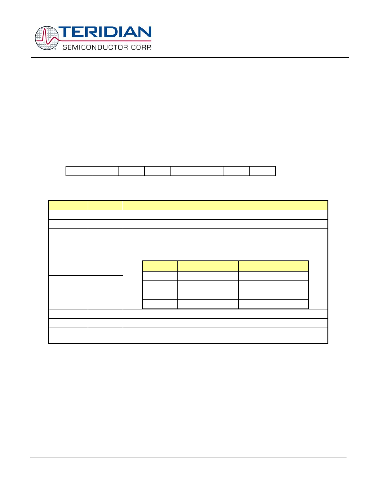
Name Location Reset value Description
P0 0x80 0xFF Port 0
SP 0x81 0x07 Stack Pointer
DPL 0x82 0x00 Data Pointer Low 0
DPH 0x83 0x00 Data Pointer High 0
DPL1 0x84 0x00 Data Pointer Low 1
DPH1 0x85 0x00 Data Pointer High 1
WDTREL 0x86 0x00 Watchdog Timer Reload register
PCON 0x87 0x00 UART Speed Control
TCON 0x88 0x00 Timer/Counter Control
TMOD 0x89 0x00 Timer Mode Control
TL0 0x8A 0x00 Timer 0, low byte
TL1 0x8B 0x00 Timer 1, high byte
TH0 0x8C 0x00 Timer 0, low byte
TH1 0x8D 0x00 Timer 1, high byte
CKCON 0x8E 0x01 Clock Control (Stretch=1)
P1 0x90 0xFF Port 1
DPS 0x92 0x00 Data Pointer select Register
S0CON 0x98 0x00 Serial Port 0, Control Register
S0BUF 0x99 0x00 Serial Port 0, Data Buffer
IEN2 0x9A 0x00 Interrupt Enable Register 2
S1CON 0x9B 0x00 Serial Port 1, Control Register
S1BUF 0x9C 0x00 Serial Port 1, Data Buffer
S1RELL 0x9D 0x00 Serial Port 1, Reload Register, low byte
P2 0xA0 0x00 Port 2
IEN0 0xA8 0x00 Interrupt Enable Register 0
IP0 0xA9 0x00 Interrupt Priority Register 0
S0RELL 0xAA 0xD9 Serial Port 0, Reload Register, low byte
P3 0xB0 0xFF Port 3
IEN1 0xB8 0x00 Interrupt Enable Register 1
IP1 0xB9 0x00 Interrupt Priority Register 1
S0RELH 0xBA 0x03 Serial Port 0, Reload Register, high byte
S1RELH 0xBB 0x03 Serial Port 1, Reload Register, high byte
USR2 0xBF 0x00 User 2 Port, high address byte for MOVX@Ri
IRCON 0xC0 0x00 Interrupt Request Control Register
PSW 0xD0 0x00 Program Status Word
WDCON 0xD8 0x00 Baud Rate Control Register (only WDCON.7 bit used)
A 0xE0 0x00 Accumulator
B 0xF0 0x00 B Register
Table 6: Special Function Registers Reset Values
Downloaded from Elcodis.com electronic components distributor
71M6403
Electronic Trip Unit
SEPTEMBER 2006
Page: 18 of 75 © 2006 TERIDIAN Semiconductor Corporation REV 1.0
Accumulator (ACC, A): ACC is the accumulator register. Most instructions use the accumulator to hold the operand. The
mnemonics for accumulator-specific instructions refer to the accumulator as “A”, not ACC.
B Register: The B register is used during multiply and divide instructions. It can also be used as a scratch-pad register to hold
temporary data.
Program Status Word (PSW):
MSB LSB
CV AC F0 RS1 RS OV - P
Table 7: PSW Register Flags
Bit Symbol Function
PSW.7 CV Carry flag
PSW.6 AC Auxiliary Carry flag for BCD operations
PSW.5 F0
General purpose Flag 0 available for user. Not to be confused with the F0 flag
in the CE STATUS register.
PSW.4 RS1
PSW.3 RS0
Register bank select control bits. The contents of RS1 and RS0 select the working
register bank:
RS1/RS0 Bank selected Location
00 Bank 0 (0x00 – 0x07)
01 Bank 1 (0x08 – 0x0F)
10 Bank 2 (0x10 – 0x17)
11 Bank 3 (0x18 – 0x1F)
PSW.2 OV Overflow flag
PSW.1 - User defined flag
PSW.0 P Parity flag, affected by hardware to indicate odd / even number of “one” bits in the
Accumulator, i.e. even parity.
Table 8: PSW bit functions
Stack Pointer (SP): The stack pointer is a 1-byte register initialized to 0x07 after reset. This register is incremented before
PUSH and CALL instructions, causing the stack to begin at location 0x08.
Data Pointer: The data pointer (DPTR) is 2 bytes wide. The lower part is DPL, and the highest is DPH. It can be loaded as a 2-
byte register (MOV DPTR,#data16) or as two registers (e.g. MOV DPL,#data8). It is generally used to access external code or
data space (e.g. MOVC A,@A+DPTR or MOVX A,@DPTR respectively).
Program Counter: The program counter (PC) is 2 bytes wide initialized to 0x0000 after reset. This register is incremented
during the fetching operation code or when operating on data from program memory.
Downloaded from Elcodis.com electronic components distributor

71M6403
Electronic Trip Unit
SEPTEMBER 2006
Page: 19 of 75 © 2006 TERIDIAN Semiconductor Corporation REV 1.0
Port Registers: The I/O ports are controlled by Special Function Registers P0, P1, and P2. The contents of the SFR can be
observed on corresponding pins on the chip. Writing a ‘1’ to any of the ports (see Table 9) causes the corresponding pin to be at
high level (V3P3), and writing a ‘0’ causes the corresponding pin to be held at low level (GND). The data direction registers
DIR0, DIR1, and DIR2 define individual pins as input or output pins (see the DIO section in On-Chip Resources for details.
Register SFR
Address
R/W Description
P0 0x80 R/W Register for port 0 read and write operations (pins DIO0…DIO7)
DIR0 0xA2 R/W Data direction register for port 0. Setting a bit to 1 means that the corresponding pin is
an output.
P1 0x90 R/W Register for port 1 read and write operations (pins DIO8…DIO15)
DIR1 0x91 R/W Data direction register for port 1.
P2 0xA0 R/W Register for port 2 read and write operations (pins DIO16…DIO21)
DIR2 0xA1 R/W Data direction register for port 2.
Table 9: Port Registers
All four ports on the chip are bi-directional. Each of them consists of a Latch (SFR ‘P0’ to ‘P3’), an output driver, and an input
buffer, therefore the MPU can output or read data through any of these ports if they are not used for alternate purposes.
Special Function Registers Specific to the 71M6403
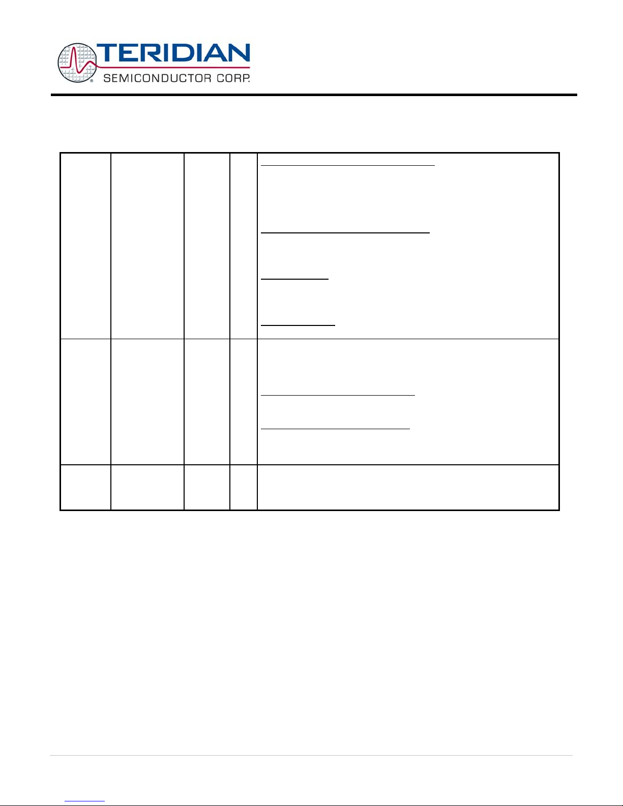
Table 10 shows the location and description of the 71M6403-specific SFRs.
Register Alternative
Name
SFR
Address
R/W Description
ERASE FLSH_ERASE 0x94 W
This register is used to initiate either the Flash Mass Erase cycle or the
Flash Page Erase cycle. Specific patterns are expected for
FLSH_ERASE in order to initiate the appropriate Erase cycle (default =
0x00).
0x55 – Initiate Flash Page Erase cycle. Must be preceded by a write to
FLSH_PGADR @ SFR 0xB7.
0xAA – Initiate Flash Mass Erase cycle. Must be preceded by a write to
FLSH_MEEN @ SFR 0xB2 and the debug port must be
enabled.
Any other pattern written to FLSH_ERASE will have no effect.
PGADDR FLSH_PGADR 0xB7 R/W
Flash Page Erase Address register containing the flash memory page
address (page 0 thru 127) that will be erased during the Page Erase
cycle (default = 0x00).
Must be re-written for each new Page Erase cycle.
EEDATA 0x9E R/W I2C EEPROM interface data register
EECTRL 0x9F R/W I2C EEPROM interface control register. If the MPU wishes to write a byte
of data to EEPROM, it places the data in EEDATA and then writes the
‘Transmit’ code to EECTRL. The write to EECTRL initiates the transmit
sequence. See the section I2C Interface (EEPROM) for a description of
the command and status bits available for EECTRL.
Downloaded from Elcodis.com electronic components distributor
71M6403
Electronic Trip Unit
SEPTEMBER 2006
Page: 20 of 75 © 2006 TERIDIAN Semiconductor Corporation REV 1.0
FLSHCRL 0xB2
R/W
W
R/W
R
Bit 0 (FLSH_PWE): Program Write Enable:
0 – MOVX commands refer to XRAM Space, normal operation
(default).
1 – MOVX @DPTR,A moves A to Program Space (Flash) @ DPTR.
This bit is automatically reset after each byte is written to flash. Writes to
this bit are inhibited when interrupts are enabled.
Bit 1 (FLSH_MEEN): Mass Erase Enable:
0 – Mass Erase disabled (default).
1 – Mass Erase enabled.
Must be re-written for each new Mass Erase cycle.
Bit 6 (SECURE):
Enables security provisions that prevent external reading of flash
memory and CE program RAM. This bit is reset on chip reset and may
only be set. Attempts to write zero are ignored.
Bit 7 (PREBOOT):
Indicates that the preboot sequence is active.
WDI 0xE8
R/W
R/W
Only byte operations on the whole WDI register should be used
when writing. The byte must have all bits set except the bits that are to
be cleared.
The multi-purpose register WDI contains the following bits:
Bit 0 (IE_XFER): XFER Interrupt Flag:
This flag monitors the XFER_BUSY interrupt. It is set by hardware and
must be cleared by the interrupt handler
Bit 1 (IE_ZP8): 0.8sec Interrupt Flag:
This flag monitors the ZP8 0.8sec interrupt. It is set by hardware and
must be cleared by the interrupt handler
INTBITS INT0…INT6 0xF8 R Interrupt inputs. The MPU may read these bits to see the input to
external interrupts INT0, INT1, up to INT6. These bits do not have any
memory and are primarily intended for debug use. Refer to the External
Interrupts description.
Table 10: Special Function Registers
Instruction Set
All instructions of the generic 8051 microcontroller are supported. A complete list of the instruction set and of the associated op-
codes is contained in the 64xx Software User’s Guide (SUG).
Downloaded from Elcodis.com electronic components distributor
Table of contents
Popular Circuit Breaker manuals by other brands


GE
GE Spectra Series AMC3FGB installation instructions

GE
GE MicroVersa Trip Plus user guide

DRIESCHER-WEGBERG
DRIESCHER-WEGBERG MINEX Addition to Operation and Assembly Instructions

Siemens
Siemens JG installation instructions

Doepke
Doepke DFS 4 B SK Series Installation and operating manual

Huanyu
Huanyu HUM8L Series Installation and operation instruction