www.ti.com
Introduction
3
SBOU161A–February 2016–Revised April 2016
Submit Documentation Feedback Copyright © 2016, Texas Instruments Incorporated
THS3215EVM and THS3217EVM
1 Introduction
This section provides a general description of the THS3215 and THS3217 devices and the EVM.
1.1 THS3215 and THS3217 Description
The THS3215 and THS3217 (THS321x) combine the key signal-chain components required to interface
with a complementary-current output, digital-to-analog converter (DAC). These two-stage devices deliver
the low-distortion, dc-coupled, single-ended signal required by a wide range of applications. The input
stage buffers the DAC resistive termination, and converts the signal from differential to single-ended with a
fixed gain of 2 V/V. The differential to single-ended output is available externally for direct use, and can
also be connected through an RLC filter or attenuator to the input of an internal output power stage (OPS).
The wideband, current-feedback, OPS provides all pins externally for flexible gain setting.
An internal 2 × 1 multiplexer (mux) to the OPS noninverting input provides an easy means to select
between the internal differential-to-single ended stage (D2S) output or an external input. More information
on the THS3215 and THS3217 can be found in their respective product data sheets, SBOS780 and
SBOS766.
1.2 EVM Description
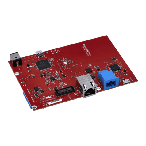
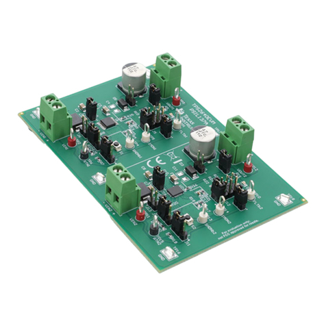
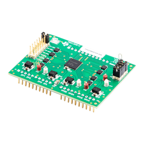
The THS321xEVM enables performance evaluation of each individual subblock within these devices. The
PCB provides various flexible options to also test either the THS3215 or THS3217 as a complete system.
The EVM provides placeholders to insert filters at different points within the system to allow for more
realistic end-application evaluation.
The following list describes key EVM components:
• Power input: ±6 VDC (typical) at +VCC (P3, TP1) and –VCC (P1, TP2)
• Common reference: GND (P2, TP3 and TP13)
• Interface to the midscale buffer input pin, VMID_IN, through J3 (TP8).
• Interface to the midscale buffer output pin, VMID_OUT, through J4 (TP9).
• Interface to the D2S noninverting signal input pin, IN+, through J1 (TP4).
• Interface to the D2S inverting signal input pin, IN–, through J2 (TP5).
• Interface to the D2S output pin, VO1, through J5 (TP14)
• Interface to the D2S reference input, VREF, through J4. SMA connector J4 is shared with the midscale
buffer output. Depending on the components populated on the board, the appropriate signal is
available at the SMA connector.
• PATHSEL control though switch CS_SW (TP12). Section 2.2 describes the operation of the switch
logic.
• Interface to the OPS external, noninverting input pin, VIN+, through J8.
• DISABLE control though switch PD_SW (TP11). Section 2.2 describes the operation of the switch
logic.
• Interface to the OPS output pin, VOUT, through J7 (TP10).
• Interface to the OPS inverting input pin, VIN–, through J6.
