Trio MS-1650B User manual
MS-1650B
DIGITALMEMORYOSCILLOSCOPE
INSTRUCTIONMANUAL
TRIO

FEATURES
This
instrumentisa combinationofanoscilloscopehavinga frequencybandofDC-10MHzanda
digital
memoryhaving
memoryabilityof8 bitsx1024wordsandwritespeedupto1 /is/word.Inputsignalcanbestoredinthememorysothat
memorysignalisdisplayedontheCRTatanytime.
The
instrumentisreadilyconnectedtoa penrecorder.Itmemorizesanddisplayssignals
prior
totriggering,instantaneous
signals,
transientwaveformsandrepetitivewaveforms.
This
modelisdesignedasa multitracememoryoscilloscopewhich
combined
with
thememory
unit
MU-165K-T)(option).
1.
Instantaneoussignals,transientwaveforms,and,.™...
repetitivewaveformscanbestoredinthememoryfor
displayingontheCRT.
2.
ByconnectingtheMU-165K-T)memory
unit
toMS-
1650B,
thelatercanbeusedfora maximumof4
traces
digital
memoryoscilloscope.
3.
Semiconductormemorycircuithavingmemoryabilityof
8
bitsx 1024wordsandwritespeedupto1 /^s/word.
4.
Theoscilloscopecoversa wideDC-10MHzband.The
controlsandswitchesoftheoscilloscopearealsoused
tostore
input
signalsinthememoryanddisplay
memorysignals.
5.
—DELAY
functionisprovidedtostoresignals
prior
to
triggering
inthememorywhichisnotpossible
with
conventionaloscilloscopes.
6.
Theautomaticfree-runfunctionrepeatswrite-inand
read-outsignalsautomatically.
By
pulling
outtheknobof
DISPLAY
TIME,
thefixed
read-outspeedisappliedupto1 jts/wordregardlessof
sweep
timeinread-outoperation.Thereforeread-out
signals
are
easy
tobe
seen.
7.
Memorysignalsarereadilydisplayedonthe
built-in
CRT
orrecordedina penrecorder.
8.
A
SMOOTHER
switchhasbeen
built-in
tomake
waveformmoreeasilyvisiblewhen
monitoring
memorizedsignalsonthe
screen;
sampleintervals
have
becomejoinedandsmooth.
9.
Real
timewaveformbeingdisplayedonthescreencan
bestoredinthememory,thusprovidingsimplified
operation.
10.
Boththerealtimewaveformandmemorysignalcanbe
displayedsimultaneously,
permitting
youtocompare
onesignal
with
theother.
11.
Memorizeddatecontentscanbekepton
hold
forover
a
weekafterpowerhasbeencutoffbecausea
memoryback-upcapacitorhasbeenbuilt-in.
Thus
you
can
storedataforasiswhileearringMS-1650B.
12.
Signalssynchronized
with
powerfrequencycanbe
displayedorstoredinthememory.
13.
Theoscilloscopecanbeusedasa X-Yscopebysimply
settingthe
DISPLAY
MODEswitchtotheX-Yposition.
14.
ByconnectingMU-165K-T),feedingits
output
into
HOR
INPUT,
X-Yoperationofrealtimewaveformand
memorywaveformcanbeexecuted.
1
5.Large
sized,
squareCRTdisplayswaveformsoverthe
entire
area
ofthe
screen.
16.
Rigidconstruction
with
diecasting
front
paneland
compactdesign.
17.
Withthejoiner
CZ-84,
MS-1650BandMU-1651
memory
unit
canbecombined
into
onebody,makingit
convenienttocarryasa dualtracememory
oscilloscope.
CONTENTS
FEATURES
2
SPECIFICATIONS
3
CONTROLS
ON
PANELS
5
Front
Panel
5
Rear
Panel
8
OPERATION
9
Oscilloscope
Operation9
DigitalMemoryOperation9
—
DELAY
Setting10
Readout
toPenRecorder10
MeasurementofInputSignalVoltage
with
PenRecorder11
MeasurementofInputSignalTime
with
PenRecorder11
Free
RunOperation11
APPLICATIONS
12
ApplicationofDigitalMemoryScope12
ApplicationofOscilloscopeOperation13
PRECAUTION
20
MAINTENANCE
AND
ADJUSTMENT
20
Maintenance20
Adjustment20
OPTION
22
2

SPECIFICATIONS
Cathode
RayTube
Type
E2713B31A
Accelerationvoltage
Approx.2 kV
Display
area
8
div
x
10div(1div
=
9.5mm)
VerticalAxis
Sensitivity
10
mV/div- 20V/div,±5%
Attenuator
10
mV/div— 20V/div,1-2-5sequence
11
ranges,fullyadjustable
Inputimpedance
1
M0,±5%22pF±3pF
Frequency
response
Oscilloscope
DC:DC-10MHz(-3dB)
(10
mV/div- 20V/div)
AC:
2 Hz-10MHz(-3dB)
(10
mV/div- 20V/div)
DigitalmemoryDC:DC-250kHz(-3dB)
AC:
2 Hz-250kHz(-3dB)
Rise
time
35
ns(Oscilloscopeoperation)
Maximum
input
voltage
600
Vp-por300V (DC+ ACpeak,at1 kHz)
Operatingmode
REAL:
Oscilloscopeoperationormemoryfree-run
DUAL:
Real
timeandmemorywaveforms,dual
trace
operation
(CHOP
modeofapprox.
500
kHz)
MEMORY:
Memorywaveformreadout
X-Y:
X-Yscopeoperation
A/DConverter
Resolution
8
bits
Conversion
system
Successive
comparisonA/Dconverter
Scale-over
8
divvertical
scale
Sweep
Circuit
Sweep
system
Triggersweep(NORM),autosweep
(AUTO)
Sweep
time
1
/zs/div— 1 s/div,±5%
1-2-5sequence
19
ranges,fullyadjustable
Magnifier
5
MAG±10%
Linearity
Less
than3%(5/ts/div— 1 s/div)
Less
than5%(1/*s/div— 2 jis/div)
Sync
Circuit
Sync
input
INT:
Vertical
input
signal
LINE:
Linefrequency
EXT:
EXT
TRIG
input
signal
Polarity
Positive
andnegative
Sync
voltage
INT:
Morethan1 divofamplitudeontheCRT
LINE:
Withinthespecifiedpowersupplyvoltage
EXT:
Morethan1 Vp-p
Sync
frequency
INT:
20Hz- 10MHz
EXT:
DC- 10MHz
External
sync
input
voltage
±15V (DC+ ACpeak)
HorizontalAxis
Operatingsystem
DISPLAY
MODEselectorswitchtoX-Yposition
Sensitivity
150
mV/div(±20%,HOR.GAINMAX)
Frequency
response
DC:
DC-1MHz(-3dB)(HOR.GAINMAX)
Inputimpedance
100
kfl±20%,35pFor
less
Maximum
input
voltage
50
V (DC+ ACpeak,HOR.GAINMAX)
MemoryUnit
Memorycapacity
1024
words(100words/div)
Writespeed
0.1ms/div— 1 s/div,13ranges(equivalentto1 /ts/word—
10
ms/word)
EXT:
RisingedgeofEXT
CLOCK
input
signal
repetition
rate
frequency:
Less
than500kHz
Highlevelpulsewidth:not
less
than1 /*s
Low
levelpulsewidth:not
less
than500ns
Rise
time,not
less
than500ns
Readout
speed
SCOPE:
Same
aswritespeed
Fixed
readout(at1 /ts/wordfor
DISPLAY
TIME
pulled
position).
...PEN:10ms/word,20ms/word50ms/word,3 ranges
:(Switchableto100ms/word,200ms/word,500ms/
wordbychangingjumperwireconnection)
EXT:
RisingedgeofEXT
CLOCK
input
signal
repetition
rate
frequency:
Less
than1 MHz
y
Inputsignal:
Highlevelpulsewidth:not
less
than
500
ns
Low
levelpulsewidth:not
less
than
500
ns
Rise
time,not
less
than500ns
Inputvoltage:TTLlevel
Maximum
input
voltage:20V (DC+ ACpeak)
Inputresistance:Approx.30kfi
Delay
-
DELAY
(0-9div,DIGSWsetting)
3
SPECIFICATIONS
Signal
Output
Display
time
The
amountoftimeforwhichmemorysignalsaredisplayedcan
bevaried
from
approx.1 toapprox.20seconds.
MemoryoutandMemoryoutforpen(OutputofonlyPENmode)
Display
time
Output
wave:
Memorywave
Outputvoltage:1.6Vp-p,
full
scale
(at8 div)
Outputresistance:Approx.430ft
Read
gate
Output
wave:
Positivepulse(1word)offinaladdress
Outputvoltage:TTLlevel
Outputresistance:Approx.220ft .
Read
gateforpen(OutputofonlyPENmode)
Outputvoltage:TTLlevel(LOWactive)
Outputresistance:220ft
Sweep
gate
Output
wave:
Positivepulsesynchronized
with
sweepsignal
Outputvoltage:TTLlevel
Outputresistance:Approx.220ft
CAL
(Calibratingvoltage)
Output
wave:
1 kHz,± 10%,squarewave
Outputvoltage:1 Vp-p±5%
Dataout
Data
output:
8
bitbinaryparallel
output,
positive
output
(TTLlevel)
Timingpulse:
Positive,
negative
output
(MOS)(TTLlevel)
Read
gateout:
Positive
output
ofthefinal-addressoneword
Outputresistance:Approx.220ft (TTLlevel)
Ext.
clock:
TTL
levelclock
input
of1 MHzorbelow
Highlevelpulsewidth:Not
less
than500ns
Low
levelpulsewidth:Not
less
than500ns
Rise
time:• Notmorethan500ns
Inputresistance:Approx.30kft
14-pincable
receptacle
#
Data
contents 14-pincable
receptacle
It
Data
contents
Pin
# 1
Data
LSB
Pin
# 8
MSB
Pin
# 2
BIT
2
Pin
# 9 TimingpulseMOS
Pin
# 3
BIT
3
Pin
# 10 TimingpulseMOS
Pin
# 4
BIT
4
Pin
# 11
EXT.
CLOCK
Pin
# 5
BIT
5
Pin
ft 12
GND
Pin
# ' 6
BIT
6
Pin
# 13
GND
Pin
# 7
BIT
7
Pin
# 14
READ
GATE
OUT
Signal
Input
Memoryin
Sensitivity:
1.6Vp-p,
full
scale
(200
mV/div)
Memory
signal
input
(3
inputsforMU-1651)
4
Frequency
response:
DC—approx.1 MHz
(-3
dB),Smoother;off
DC—
approx.150kHz
(-3
dB),Smoother;on
Inputimpedance:Approx.60kft
Maximuminputvoltage:20Vp-por10V (DC+ ACpeak)
Intensity
Modulation
Inputvoltage
TTL
level(Intensityincreasing
with
morepositive
levels)
Inputimpedance
Approx.1 5 kft
Inputfrequency
DC
- 1 MHz
Maximuminputvoltage
50
V (DC+ ACpeak)
PowerRequirement
Voltage100/120/220/240V,± 10%,50/60Hz
Power
consumptionApprox.60W
Dimensions
Width284mm(328mm)
Height138mm(153mm)
Depth400mm(463mm)
() dimensionsincludeprotrusionsfrom
basic
case
outlinedimensions
WeightApprox.9 kg
OperatingTemperature
Operatingtemperatureforguaranteedspecification:0°~40°C
Full
operatingtemperature:0°~50°C
Accessory
Probe
(PC
—22)1 piece
Attenuation1/10
Inputimpedance10Mft
Less
than18pF
Replacement
fuse1.5A,2 pieces
0.7A,2 pieces
Instructionmanual1 copy
AC
cord1 piece
Digital
output
plug1 piece
Option
Joiner
CZ-84
PINCONFIGURATION

CONTROLS
ON
PANELS
CONTROLS
ONFRONTPANEL
1.
POWER/SCALE
ILLUM
Power
switchand
scale
illumination
control.Fully
counterclockwise
rotation
ofthis
control
turnsoff
oscilloscope.Clockwise
rotation
turnsonoscilloscope.
Furtherclockwise
rotation
ofthis
control
increasesthe
illumination
levelofthe
scale.
2.
LEDPILOTLAMP
Lightswhenoscilloscopeisturnedon.
3.INTENSITY
Intensitycontrol.Adjuststhebrightnessofspotand
waveformsfor
easy
viewing.A
left
turn
allowsthe
waveformstodisappear.
4.
TRACE
ROTATION
This
control
isusedtoeliminateinclinationofhorizon-
taltrace.
5.
FOCUS
Spotfocus
control
to
obtain
optimum
waveformac-
cordingtobrightness.
6.CAL
Provides
1 kHz,1
volt
peak-to-peaksquarewave
out-
putsignal.Thisisusedforcalibrationofthevertical
amplifierattenuatorsandtocheckthefrequencycom-
pensationadjustmentoftheprobesused
with
the
oscilloscope.
7.GNDTERMINAL
Earth
terminaloftheoscilloscope.
8.VOLTS/DIV
Verticalattenuatorcalibratedinvoltageperdivision.In
theextremeclockwise(CAL)position,theverticalat-
tenuatoriscalibrated.
Select
the
position
ofthe
control
accordingtothe
magnitudeof
input
voltageto
obtain
the
optimum
waveform.
Verticalsensitivityiscalibratedin11steps
from
0.01
to20voltsperdiv.
9.VARIABLE
Fine
adjustment
control
ofverticalsensitivity.Thesen-
,-*'sitivity
within
the11rangesof
VOLTS/DIV
(8)iscon-
tinuouslyadjustable.Theextremeclockwise(CAL)
position
isusedtocalibratetheverticalattenuator.
10.t POSITION
The
rotation
ofthis
control
adjustsvertical
position
of
real
time
waveformasdesired.A
right
turn
ofthiscon-
trol
will
shiftthereal
time
waveformupward,andvice
versa.
5
CONTROLS
ON
PANELS
11.
MEMORYPOSITION,PUSHMEMORY
FREEZE
Vertical
positionofmemorywaveformadjustment
knob.
A
right
turn
ofthiscontrolwillmovethememory
waveformupward,andvice
versa.
Whenthiscontrolispushed,onlythemain
unit
memorybecomes
FREEZE;
inwritecondition,
memorizedwaveformispreservedandcannotwritein
memory./"
Atpulledoutcondition,write-intomain
unit
memory
becomes
possible.
12.
DISPLAY
MODE
This
switchselectsthemodesofverticalandhorizon-
taloperations.
REAR:
Fornormaloscilloscopeoperation.Also,us-
edtowritea signalinmemory.
DUAL:
This
modeforswitchingbetweenrealtime
waveformandmemorywaveform
through
CHOP
operationatapprox.500kHzand
monitoring
both
waveform.Write-into
memorycanonlybeaccomplished
through
manualoperationof
START
(16)switch.
MEMORY:
Forreadoutofmemorywaveform.
X-Y:
ForX-Yoscilloscope.
13.
AC-GND-DC
Vertical
input
selectorswitch.ACpositionblocksDC
componentof
input
signal.GNDpositionopenssignal
input
pathandgroundsamplifier
input.
DCposition
directs
input
ofACandDCcomponentstoamplifier.
Whenthe
DISPLAY
MODEissetto
REAL
or
DUAL,
a
trace
appearsonthescopeinGNDpositionofAC-
GND-DC
switchregardlessofthepositionofthe
PULL
AUTO
(27).
14.INPUT
Vertical
input
terminal.
15.
CLOCK
INT/EXT:
Clockselectorswitch.Write-inandread-out
occures
viatheclock
inputted
attheEXT
CLOCK
(35)terminal.Inthisposition,the
waveformonthescopecannotbe
syn-
chronized.
INTpositionisusedforwriteand
readout.Therearetwofunctions,
SCOPE
andPEN(readoutonly)
SCOPE/PEN:
Memoryreadoutmodeselectorswitch.
In
SCOPE
position,readoutonthescreenis
effectedrepeatedly.
Inpenposition,readouttoMEMORYOUT
terminaliseffectiveeachtime
START
is
depressed.
Forwritemode,usethe
SCOPE
position.
The
memorydata
from
theinitialaddressto
finaladdressarereadoutoncebypressing
thisswitch.
16.
START
A
pushbuttonswitchtowrite
input
signalinmemory.
To
usethisswitch,set
DISPLAY
MODEto
REAL
or
DUAL,
CLOCK
toINTand
SCOPE,
and
SWEEP
TIME/DIV
to0.1ms-1s.InthePENmode,thisswitch
functionsasthePEN
START
push
button
switch.
17.
TRIGGER
POINT
-DELAY
(DIV)
This
switchisusedtowrite
input
signalinmemory
beforetriggersignalisgenerated.Thesettingrange
covers
from
0 div.to9 div.1 div.represents100
wordsinmemory.
(Refer
to
"-DELAY
Setting"onpage10)
18.WRITE(LED)
Red
LEDlightswhile
input
signalisbeing
written
in
memory.
19.
READ
(LED)
Green
LEDlightswhilememorydataisbeingreadout.
20.MEMORYOUTPUT
Memorydata
output
terminal.Readoutspeedisvaried
accordingto3 readoutmodes,
SCOPE,
PENandEXT
CLOCK.
21.
SWEEP
TIME/DIV
Horizontalsweeptimeselector.Itselectssweeptimes
of1 fis to1 s in19steps.The1 /is-50/is rangeisus-
edforrealtime.
22.
VARIABLE/HOR.
GAIN
Used
forfineadjustmentofsweeptime.Continuous
adjustmentbetween19rangesof
SWEEP
TIME/DIV
(21)
ispossible.Sweeptimeiscalibratedattheex-
tremeclockwiseposition
(CAL).
Whenthe
DISPLAY
MODE
issettoX-Y,thesignal
from
theHOR
INPUT
is
attenuatedby
SWEEP/TIME
DIV.control.
23.
POSITION
Rotationadjuststhehorizontalpositionoftraceas
desired.
Clockwise
rotation
shiftsthetracetothe
right
andcounterclockwiserotation,tothe
left
24.FINE
PULL
X5MAG
Horizontalpositionfineadjusterandsweepmagnifica-
tion
selectorswitch.Pulltheknobandthetraceis
magnifiedfivetimesaslargeinthe
left
and
right
direc-
tions.Brightnessisslightlydecreased.
Inputsignalstoredinthememoryisnotmagnified
even
intheX5MAGposition.
6
CONTROLS
ON
PANELS
25.
SOURCE
Sync
sourcevoltageselectorswitchforthreefunctions,
INT
(internal
sync),
LINE
(50/60Hz
sync)
andEXT(exter-
nal
sync).
INT:
Sweepis
triggered
byvertical
input
signal.
LINE:
Sweepis
triggered
by50/60Hzpowerfre-
quency.
EXT:
Sweepis
triggered
byvoltageappliedto
EXT
TRIG
terminalandDCcomponent.
26.
SLOPE
Sync
polarity
selectorswitch.Inthe" + " position,
sweep
is
triggered
with
risingslopeof
input
waveform,
andinthe"
—
" position,
with
fallingslopeof
input
waveform.
27.
LEVEL,
PULL
AUTO
Triggeringlevel
control
adjustssyncphasetodeter-
minethestarting
point
ofsweepontheslopeof
trigger
signalwaveform.By
pulling
theknobtowardyou,auto
sweep
iseffected;thesweepissetinfree-runstate
andthetraceisdisplayedonCRTevenwhenno
trigger
signalispresent.When
trigger
signalispresent,sweep
is
startedsothe
triggering
levelcanbeadjusted.
28.TRIG'D
Sync
indicationlamplightswhensyncsignalistrig-
gered.
Checkthislamplightswhen
writing
input
singal
tomemory.
The
lampmay
light
intheGND
position
oftheAC-
GND-DC
(13).Thisisnormalandisnotanindication
that
the
unit
isdefective.
29.EXTTRIG
Input
terminalforexternal
trigger
signal.Externaltrig-
gersignal(1Vp-porhigher)shouldbeapplied
with
SOURCE
switchsettoEXT.
30.HORINPUT
Input
terminalforexternalhorizontalsignal.
DISPLAY
MODE
switchshouldbesettoX-Y.
31.
DISPLAYTIME
Store
andread-outoperationareautomatically
repeatedwhenthisknobispulledout(freerun
fuction).Thedisplay
time
isabout1 secondwhenthe
knobis
fully
settothe
left
andabout20secondswhen
itis
fully
settothe
right.
This
function
iseffectiveonly
whenthe
DISPLAY
modeis
REAL.
32.
PEN
SPEED
Selects
thememoryreadspeedinthePENmode
from
amongthreespeeds:10to50ms/word.Thisswitch
functionsregardlessofthe
position
of
SWEEP
TIME/DIV
(21).
7

CONTROLS
ON
PANELS
CONTROLS
ON
REAR
PANEL
33.
SWEEP
GATE
OUT
Sweep
gatesignal(positivepulse)isavailableatthis
terminal.
34.
READ
GATE
OUT
Positive
pulseforonewordoffinalmemoryaddressis
available
atthisterminal.
The
signalcanbeusedasa stopsignalwhena pen
recorderis
used.
35.
EXT
CLOCK
Inputterminalforexternalclock.
CLOCK
switch(15)shouldbesettoEXT.
36.Z-AXISINPUT
Intensitymodulationterminal.Intensityismodulated
atTTLlevel.
37.SMOOTHER
WhenslidedthisswitchtoONside,thesample
waveformbecomesjoinedandmakesvisible.
38.GND
Groundterminal.Oscilloscope
chassis
ground,and
earthground.
39.MEMORYINPUT
Three
input
terminalsformemorizedsignalswhencon-
nectingMU-1651memory
unit
andusingasa mutiple
trace
memoryoscilloscope.
40.CONTROLOUTPUT
Controlsignal
output
terminalformemorizedsignal
whenconnectingMU-1651memory
unit
andusingas
a
mutipletracememoryoscilloscope.
41.
DATAOUT
Outputterminalformemorydata(8bit
BINARY)
and
timing
signal.
42.
POWERCONNECTOR
For
connectionofaccessorypowercord.
43.
FUSE
HOLDER
For
100/120V operation,usea 1.5Afuse.For
220/240
V operation,besuretousea 0.7Afuse.
44.POWER
VOLTAGE
SELECTOR
Set
theselectortothepositioncorrespondingtothe
correctACpowervoltage,100/120/220/240V.
45.
CORD
REEL
Windthepowercordinthereelwhentheoscilloscope
needs
tobetransportedoritistobe
left
unused.
46.MEMORY(FORPENOUT)
This
output
terminalisonlyeffectiveforPENmode.
When
START
(16)ispressed,
output
ofthesamedata
as
thatofMEMORY
OUTPUT
(20)starts.
47.
READ
GATE
(FORPENOUT)
This
isvalidonlyinPENmode.
This
terminaloutputs
thesamesignalasthat
READ
GATE
(34).
This
output
signal
dropstotheGNDleveltostartpenoperation,
and
rises
totheH leveltostoppenoperationwhen
readingisfinished.Theterminalisgroundedinthe
SCOPE
mode.
8
OPERATION
OSCILLOSCOPE
OPERATION
Refer
totheprevioussection"Controlson
Panels".
Before
operatingtheoscilloscope,settheswitchesandcontrols
as
follows:
Switches
andControls Position
1.
POWER/SCALE
ILLUM
OFF
3.
INTENSITY
Center
(slightlyright)
5.
FOCUS
Center
8.
VOLTS/DIV
20
V
9.
VARIABLE
Full
clockwise
10.
t
POSITION
Center
12.
DISPLAY
MODE
REAL
13.
AC-GND-DC
GND
21.
SWEEP
TIME/DIV
1
ms
22.
VARIABLE
Full
clockwise
23.
<o
POSITION
Center
24.
FINE
PULLx
5 MAG
Center
(PUSH)
25.
SOURCE
INT
26.
SLOPE
+
27.
LEVEL
Center
(PULL)
AUTO
31.
DISPLAY
TIME
PUSH
1.
Connectthesuppliedpowercordtothepowercon-
necter.Theoscilloscopeisfactoryadjustedtooperate
onAC240V.
2.
Turnthe
POWER
switch(1)toONandthe
POWER
lamp
(2)
will
light.
Thenhorizontaltracewillappear.If
horizontaltracedoesnotappearatthecenterofthe
screen,
adjusttheT
POSITION
(10).
3.
Adjusttheintensitybythe
INTENSITY
(3).Ifthetraceis
unclear,
adjustthe
FOCUS
(5).
4.
Ifthetraceisinclined,adjustthe
TRACE
ROTATION
(4).
5.
Setthe
AC-GND-DC
(13)toACorDCpositionandapp-
ly
input
signaltothe
INPUT
(14).Turnthe
VOLTS/DIV
(8)
clockwisetoobtain
optimum
waveform.
6.
Ifthewaveformisrunningandnottriggered,
turn
the
LEVEL
(27).Bypushingthe
LEVEL
knob,theautofunc-
tion
isreleased.Thewaveformdisappearswhenthe
knobisturnedclockwiseorcounterclockwiseandap-
pears
againattheapproximatemidpositionofit.Turn
theknob
until
optimum
triggering
levelisobtained.
7.
Whenthesignalvoltageismorethan0.01V and
waveformdoesnotappearonthe
screen,
the
oscilloscopemaybecheckedbyfeeding
input
from
the
CAL
(6)terminal.
Since
thecalibrationvoltageis1 Vp-
p,thewaveformbecomes5 divatthe0.2V positionof
the
VOLTS/DIV.
8.
InmeasuringDCcomponent,setthe
AC-GND-DC
(13)
toDC.Ifitcontainspositive(+ } potential,the
waveformmovesupward.Ifnegative
( —)
potentialis
contained,thewaveformmovesdownward.Thezero
potentialcanbecheckedattheGNDposition.
DIGITAL
MEMORYOPERATION
Set
theswitchesandcontrolsasfollowsbeforeusingthe
digital
memory:
Otherknobsandcontrolsarethesameinfunctionasthose
ofoscilloscopeoperation.
Switches
andControls Position
11.
MEMORY
POSITION
Pull
mechanical
center
12.
DISPLAY
MODE
REAL
orDUAL
15.
CLOCK
INT/SCOPE
17.
TRIGGER
POINT
0
21.
SWEEP
TIME/DIV
0.1ms— 1 s
27.
LEVEL
NORMAL
(PUSH)
31.
DISPLAY
TIME
PUSH
32. PEN
SPEED
10
ms,20ms,
50
ms/word
[A]ManualOperation
1.
Operatetheoscilloscopeanddisplaya triggeredsignal
onthe
screen.
2.
Depressthe
WRITE
START
(16)andthe
WRITE
(18)
lampwill
light.
3.
Whenthe
WRITE
lampgoesoff,the
READ
(19)lamp
beginstoflicker.
4.
Setthe
DISPLAY
MODE(12)toDUALor
MEMORY,
and
memorywaveformwillbedisplayed.IntheDUALmode,
therealtimewaveformoverlaps
with
thememory
waveform.ByadjustingtheT
POSITION
(10)or
MEMORY
POSITION
(11),
both
waveformscanbe
observed.
5.
Whenobservingmemorywaveform,itisnotnecessary
toadjustthe
VOLTS/DIV
(8)and
SWEEP
TIME/DIV
(21).
The
VOLTS/DIV
doesnotchangetheamplitudeof
thememorywaveform.The
SWEEP
TIME/DIV
changes
onlythereadoutspeed;thememorywaveformremains
unchangedonthe
screen.
[B]
Automaticwrite-in,read-outOperation
Pull
outthe
DISPLAY
TIME
(31)forwardyouandsetthis
controlatabout9 o'clockpositionin
FREE
RUNstate.
Refer
to
FREE
RUNfunctiononpage11.
9
OPERATION
—
DELAY
Setting
Withconventionaloscilloscopes,itisnotpossibleto
observe
a tracebefore
triggering
signalisdeveloped.
This
oscilloscopehas"
—
DELAY"
functiontostorea
waveforminmemorybefore
triggering
signalisdeveloped,
thus
permitting
a widevarietyofapplications.Thenumbers
indicatedbythesetting
TRIGGER
POINT
switch(17)cor-
respondtothehorizontal
scale
divisionssothattrigger
pointscanbeeasilycheckedonthescope.
The
diagrambelowshowsthe
—DELAY
pointsindicatedby
thesetting
TRIGGER
POINT
switch(17).
Read-outtoPenRecorder
This
oscilloscopepermitsanyhighspeedtracestobe
storedinmemoryandconverted
into
slowspeedtime
base
whicha recorderisableto
follow.
Thus,
itispossibleto
recorda memorydataina recorderata speedsuitableto
therecorder'sresponse.
The
standardreadoutspeedsare10ms/word,20ms/word
and50ms/wordbutcanbeappliedto100ms/word,
200ms/wordand500ms/wordbychangingtheconnec-
tionsofthejumperwireincontrolcircuitboard(Fig.2).
To
recorda memorydataina penrecorder,performthe
following
procedures:
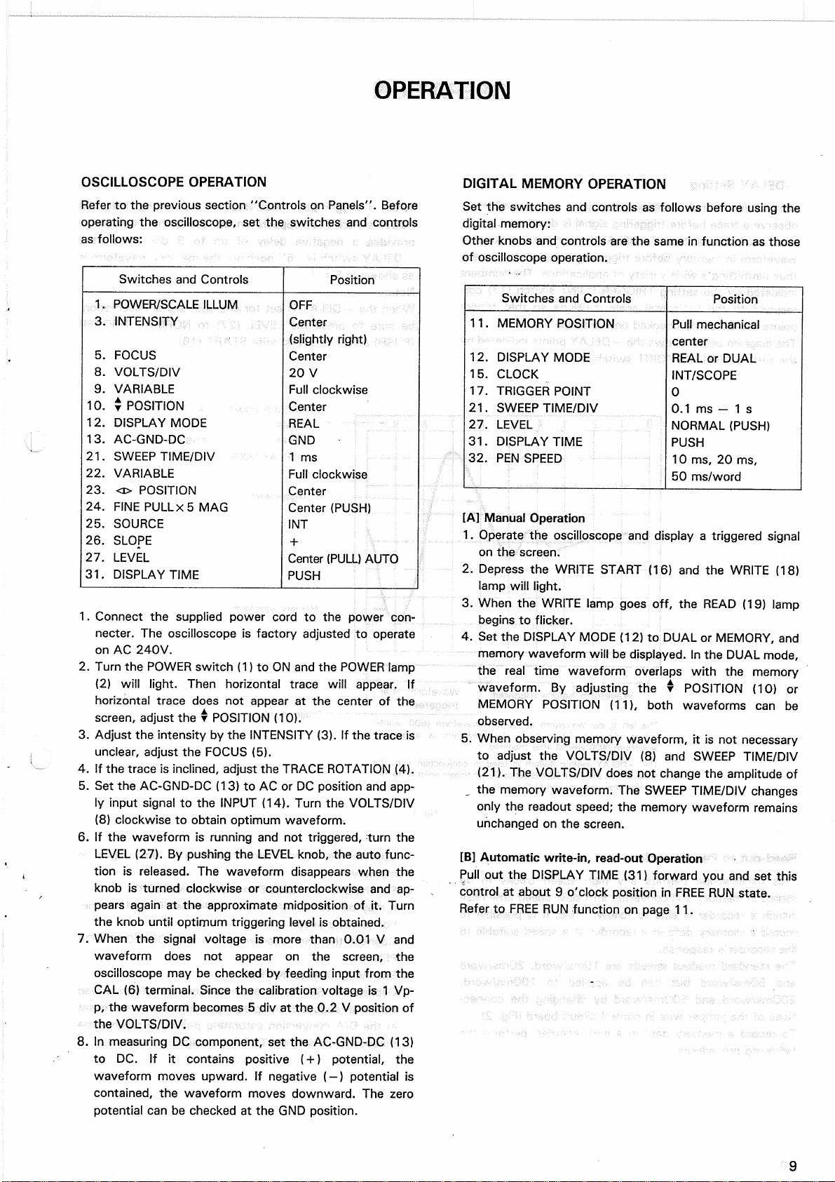
Whena trigger
point
indicatedbythesetting
TRIGGER
POINT
switch(17)appearsonthe
scale,
theoscilloscope
providesa negativedelayofupto9 div.Whenthe
—
DELAY
switchis"6"position,thememorywaveformis
as
showninFig.1.
Note:
Whenthe
—DELAY
issetforone-shotsignalobservation,
besureto
press
the
LEVEL
(27)toNORMAL
TRIGGER
(PUSH)
andthen
press
write
START
(16)
1.
Operatethe
digital
memoryandwrite
input
signalin
memory.
2.
Setthe
DISPLAY
MODEtoDUALor
MEMORY.
Itmaybesetto
REAL
modewhilethe
FREE
RUNfunc-
tion
isbeing
used.
3.
Connectthepenrecordertothe
MEMORY
OUTFOR
PEN.
4.
Setthe
CLOCK
to
INT/PEN.
5.
Depressthe
START,
andthememorywaveformisread
out.Thereadoutiscompletedat1024wordsandisset
intheD/Aconversionsaturating
point.
Toresumethe
readout,depressthe
START
onceagain.
Memorywaveform
The
left
6 divwaveformismemorywaveform(600words)
beforetriggered.The
right
4 divwaveformisa memory
waveform(400words)aftertriggered.
The
—DELAY
settingswitchisusedinconjunction
with
the
scale.
Whenthe—
DELAY
issetto6,thetrigger
point
isthe6th
division
from
the
left
endofthe
scale.
Trigger
point
10
«
TRIGGER
POINT
6
SLOPE
+-
LEVEL
PUSH
DISPLAY
MODE
MEMORY
Triggerlevel
Waveformbeforetriggered Waveformafter
triggered
Fig.
1

OPERATION
Fig.
2
MeasurementofInputSignalVoltagewithPenRecorder
To
obtain
input
signalvoltageV
from
thewaveformrecordedbythepenrecorder,usethe
following
equation:
Pen
recorder
input
level(V/cm)x Recordedamplitude(cm)
V(v)
= x Write
input
level(V/div)
0.2(V/div)
MeasurementofInputSignalTimewithPenRecorder
To
obtainwritesignaltimeT
from
thewaveformrecordedbythepenrecorder,usethe
following
equation:
Pen
recorderfeedspeed
(sec/cm)
T(sec/cm)
= x Writespeed(sec/div)
Readout
speed(sec/div)
FREE
RUNfunction
This
functionisusedtoautomaticallyrepeatstoreandread
operations.Theperiodforwhichthe
input
waveformdata
is
storedinthememorycanbevaried
from
aboutA to20
seconds
with
the
DISPLAY
TIME
knob;thisisconvenient
whenitisnecessarytoobserveconsecutivephenomena
without
observerintervention.
By
pulling
the
DISPLAY
TIME
knob
(REAL
position),the
FREE
RUNfunctions.
Depressing
the
DISPLAY
TIME
knobresetsthefreerun
functionand
sets
the
REAL
mode.
Pressing
andholdingthewrite
START
button
forone
repetition
ofthestoreandread
input
waveformdatacycle
temporarilysuspendstheautomaticfreerunfunctioninthe
memoryreadstate.
Press
andthen
pull
the
DISPLAY
TIME
knob,orsetthe
DISPLAY
MODEswitchtotheMEMORY
(or
DUAL)
position,thentothe
REAL
positiontorestartthe
automaticfreerunfunction.
Note:
The
FREE
RUNfunctionwillnotalwaysstartby
turning
onthe
POWER
switch
with
the
DISPLAY
TIME
knobin
the
pull
outposition.
11
Control
board
Power
supply
board
Bottom
view
C
10ms
/ word
10ms^
20ms/
word
l^50ms/ word
C100
ms/ word
100
ms•<200ms/ word
1^500ms/ word

APPLICATIONS
APPLICATIONS
OFDIGITALMEMORY
SCOPE
This
instrumenthasa
digital
memory
function
toanalyze
variouswaveformswhichisnotpossible
with
conventional
oscilloscopes.
The
following
showstypicalexamplesofthe
use
ofthe
digital
memoryscope.
ApplicationtoElectricCircuitMeasurementofrelay
chattering
The
operating
method
isthesameas
noted
intheprevious
section.
Load
Device
under
test
SetLEVEL
knob
toNORMAL
Fig.
3 . Memorizingthetransientphenomenonof
mechanical
impactwaveforms
Contact
INPUT,
Relay
Fig.
4.Measurementofrelaychattering
SettingoftheDigital
Memory
Scope
1.
Connectthedetectortothedeviceundertest,thencon-
nectthe
output
ofthedetectortothe
input
ofthescope
through
theamplifierso
that
the
output
levelcanbeset
tothe
input
levelofthescope.
2.
Operationofthescope
(1)
Input
Selector:SettoACorDC
position
(setto
either
position
accordingtothe
input
signalbeing
applied).
(2)DISPLAY
MODE:Setto
REAL
orDUALposition.
Observe
thesignal
from
thedeviceundertestusingthe
oscilloscope
(REAL
MODE)andsetthe
input
level,trig-
ger
point
andsweepspeedasshownbelow.
LEVEL
knob:NORMAL— The
input
signalissweptonce
andstops.
Verticalattenuator(VOLTS/DIV):Anyposition.
SWEEP
TIME/DIV:Any
position
between0.1s and
0.1ms.
CLOCK:
INT
SCOPE
PEN:
SCOPE
TRIGGER
POINT(-DELAY/DIV):This
digital
switchisused
torecorda signal
prior
to
triggering
andshouldbe
set
to0 — 9 div.
3.
Aftersettingtheaboveswitches,
turn
the
START
switchtoON.The
WRITE
LED(red)
will
light
toindicate
that
the
input
signalisinstandbymode.Thesignalis
nowreadytobememorized.
4.
Next,applythesignal
from
thedeviceundertesttothe
detector.
Test
thedata.Whenthe
output
levelofthe
detectorreachesthevaluesetbythe
TRIG
LEVEL,
the
signal
from
that
point
isstoredinthememory.
5.
Tocheckthewaveformbeingstored,setthe
DISPLAY
MODE
switchtoDUALorMEMORYposition.
Datarecording
with
penrecorder
Connect
to
READ
outterminal
'attherearpanel
Recorder
START/STOP
controlterminal
"FOR
PEN
range
Pen
Recorder
(X-Y
Recorder)
Memory
OUT
terminal
To
recordmemorydata
with
penrecorder(X-Yrecorder),
makeconnectionasshowninFig.7 andoperatethescope
as
follows:
1.
Changethe
position
ofthe
CLOCK
modeswitch
from
SCOPE
toPEN(Setthe
CLOCK
toINTandthe
DISPLAY
MODE
toDUALor
MEMORY).
Itmaybesetto
REAL
whilethe
FREE
RUN
function
ison.
2.
SetthePEN
SPEED
knobtoeitherthe10,20or50ms
position.
3.
Depressthe
START
(memorydatais
outputted
wordby
word).
Note
Ifthepenrecorderhasanexternal
START/STOP
control
terminal,the
timing
pulse
output
isobtained
from
the
READ
OUTFOR
PEN
terminal(BNC)attherearpanel.The
START
signalis
outputted
inGNDlevel.
To
obtain
theamplitudecycleof
input
signal
from
the
waveformrecordedbythepenrecorder,refertothesection
"Operation".
12
Detector
AMP]
,INPUT|
Set
LEVEL
knob
toNORMAL
*Set
DELAY
to2 ~ 5 divisions.
Y
inputterminal
Fig.
5.Datarecordingwithpenrecorder

APPLICATIONS
Readout
from
external
CLOCK
Whenthescopeisoperated
with
external
CLOCK,
itfunc-
tionsonlyasa readoutscopeanddoesnot
function
asa
write-inscope.Thereadout
function
isusefulwhenobser-
vinga magnifiedwaveform(magnifiedtoHORx5MAG).
Inthis
case,
the
SWEEP
TIME/DIV
isdisabledsothe
waveformdisplayremainsthe
same,
except
that
the
sweep
speedisvaried.Itisalsousedtoreadoutthe
MEMORY
OUTsignaltoanexternaldeviceata speedother
thanthescope'sreadoutspeed(INT
CLOCK),
ortotransfer
thedatawordbywordbyconnecting
digital
output,
tothe
externaldevice(seeFig.6).
Digitaloutput
(option)
(8
pitBinary)
Digitaldevice
Set
CLOCK
MODE
toEXT
Fig.
6.Transferofdigitalsignaldatawordbyword
toanotherdigitaldeviceusingexternalclock
APPLICATIONS
OF
OSCILLOSCOPE
OPERATING
Phase
Measurement
Phase
measurementsmaybemade
with
anoscilloscope.
Typical
applicationsareincircuitsdesignedtoproducea
specific
phaseshift,andmeasurementofphaseshift
distortion
inaudioamplifiersorotheraudionetworks.
Distortionsduetonon-linearamplificationisalsodisplayed
intheoscilloscopewaveform.
A
sinewave
input
isappliedtotheaudiocircuitbeing
tested.Thesamesinewave
input
isappliedtothevertical
input
oftheoscilloscope,andthe
output
ofthetestedcir-
cuitisappliedtothehorizontal
input
oftheoscilloscope.
The
amountofphasedifferencebetweenthetwosignals
can
becalculated
from
theresulting
Lissajous'
waveform.
To
makephasemeasurements,usethe
following
pro-
cedures
(refertoFig.7).
Audiosignal
generator
Audio
network
beingtested
Load
Adjust
V.gainfor
convenientviewing
height
X-Y
•
AC-
t3"
Fig.
7 Typicalphasemeasurement
13
(Clock
of
less
than1 MHz)
EXT
CLOCK
terminalat
therearpanel

APPLICATIONS
1.
Usinganaudiosignalgenerator
with
a puresinusoidal
signal,
applya sinewavetestsignaltotheaudionet-
workbeingtested.
2.
Setthesignalgenerator
output
forthenormaloperating
level
ofthecircuitbeingtested.Observethecircuit's
out-
putontheoscilloscopeandifthetestcircuitisoverdriven,
thesinewavedisplayisclippedandthesignallevelmustbe
reduced.
3.
ConnecttheHOR.INPUTtothe
output
ofthetestcir-
cuit.
4.
Setthe
DISPLAY
MODEtoX-Y.
5.
Connecttheprobetothe
input
ofthetest
circuit.
6.
Adjusttheverticalandhorizontalgaincontrolsfora
suitableviewing
size.
7.
SometypicalresultsareshowninFig.8.Ifthetwo
signals
areinphase,theoscilloscopetraceisa straight
line.Iftheverticalandhorizontalgainareproperlyad-
justed,thislineisat45°angle.A 90°phaseshiftpro-
duces
a circularoscilloscopepattern.
Phase
shiftof
less
(ormore)than90°producesanelliptical
Lissajous'
pat-
tern.Theamountofphaseshiftcanbecalculatedbythe
method
showninFig.9.
When,
inparticular,theMU-1651memory
unit
iscon-
nectedanditsMEMORYOUTisappliedtoHOR
INPUT,
thephaseoftwomemorizedwaveformscanbe
calculated.
WhenthreeMU-165K-T)unitsareused,X-Yoperation
betweeneachtracecanbeexecuted.Atsuchtimes,
turn
off
SMOOTHER
switch(37).Referto
INSTRUC-
TION
MANUALonMU-1651indetails.
Fig.
8.Typiclphasemeasurementoscilloscope
displays
B
SINE
0 •= —
A
WHERE
<t> = PHASEANGLE
Frequency
Measurement
1.
Connectthesinewaveofknownfrequencytothever-
tical
input
oftheoscilloscopeandsetthe
DISPLAY
MODE
switchtoX-Y.
2.
Connectthevertical
input
probetothesignaltobe
measured.
3.
Adjustthevertical
input
andhorizontal
input
forproper
sizes.
4.
Theresulting
Lissajous'
patternshowsthe
ratio
between
thetwofrequencies(seeFig.10).
UNKNOWN
FREQUENCY
RATIOOF
TO
VERTICAL
INPUT.UNKNOWN
STANDARD
FREQUENCY
TO
TO
HORIZONTALINPUTSTANDARD
SEE
NOTE
SEE
NOTE
NOTE
ANYONEOF
THESE
FIGURES
DEPENDINGUPON
PHASE
RELATIONSHIP
Fig.
10.
Lissajous'
waveformsusedforfrequency
measurement
14
Fig.
9 . Phaseshiftcalculation
W: 1
1
: 1
1V4
: '1
6
: 1
NO
AMPLITUDE
DISTORTION
NO
PHASESHIFT
•
AMPLITUDE
DISTORTION
NO
PHASESHIFT
180
OUT
OF
PHASE
NO
AMPLITUDE
DISTORTION
PHASESHIFT
AMPLITUDE
DISTORTION
PHASESHIFT
90
OUT
OF
PHASE

APPLICATIONS
AmplifierSquareWaveTest
Introduction
A
squarewavegeneratorandtheoscilloscopecanbeused
toobservevarioustypesof
distortion
presentinelectriccir-
cuits.
A squarewaveofa givenfrequencycontainsa large
numberofoddharmonicsofthatfrequency.Ifa 500Hz
square
waveisinjected
into
a circuit,frequencycom-
ponentsof1.5kHz,2.5kHzand3.5kHzarealsoprovid-
ed.
Since
vacuumtubesandtransistorsarenon-linear,itis
difficult
toamplifyandreproducea squarewavewhichis
identicaltothe
input
signal.Interelectrodecapacitances,
junctioncapacitances,straycapacitancesaswellasnar-
rowbanddevicesandtransformerresponsearethefactors
whichprevent
faithful
responseofa squarewavesignal.A
welldesignedamplifiercanminimizethe
distortion
caused
bytheselimitations.Poorlydesignedordefective
amplifierscanintroduce
distortion
tothe
point
wheretheir
performanceisunsatisfactory.Asstatedbefore,a square
wave
containsa largenumberofoddharmonics.Byinjec-
ting
a 500Hzsinewave
into
anamplifier,wecanevaluate
amplifierresponseat500Hzonly,butbyinjectinga
square
waveofthesamefrequencywecanunderstand
howtheamplifierwouldresponseto
input
signals
from
500
Hzuptothe
1
5thor21stharmonic.
The
needforsquarewaveevaluationbecomesapparentif
we
realizethatsomeaudioamplifierswillberequiredduring
normaluseto
pass
simultaneouslya largenumberof
dif-
ferentfrequencies.Witha squarewave,wecanevaluate
thequalityof
input
and
output
characteristicsofa signal
containinga largenumberoffrequencycomponentssuch
as
complexwaveformsofmusicalinstrumentsorvoices.
The
squarewave
output
ofthesignalgeneratormustbe
extremelyflat.Theoscilloscopevertical
input
shouldbeset
toDCasitwillintroducetheleastdistortion,especiallyat
lowfrequencies.
Because
oftheharmoniccontentofthe
square
wave,
distortion
willoccurbeforetheupperendof
theamplifierbandpass.
Itshouldbenotedthattheactualresponsecheckofan
amplifiershouldbemadeusinga sinewavesignal.
This
is
especially
important
inan
limited
bandpassamplifiersuch
as
a voiceamplifier.
The
squarewavesignalprovidesa quickcheckofamplifier
performanceandwillgiveanestimateofoverallamplifier
quality.Thesquarewavealsowillrevealsomedeficiencies
notreadilyapparentwhenusinga sinewavesignal.
Whethera sinewaveorsquarewaveisusedfortestingthe
amplifier,itis
important
thatthemanufacturer'sspecifica-
tionsontheamplifierarebasedoninordertomakea better
judgementofitsperformance.
Testing
Procedure(refertoFig.11):
1.
Connectthe
output
ofthesquarewavegeneratortothe
input
oftheamplifierbeingtested.
2.
Connectthevertical
input
probeoftheoscilloscopeto
the
output
oftheamplifier.
3.
IftheDCcomponentoftheamplifier
output
islow,set
the
AC-GND-DC
switchtoDCpositiontoallow
both
the
AC
andDCcomponentstobeviewed.However,theAC
positionmaybeusedtoobservetheACcomponenton-
ly,
though
thiswillreducetheaudiofrequencycontent
of
less
than5 Hz.
4.
Adjusttheverticalgaincontrolsfora convenientview-
ingheight.
5.
Adjustthesweeptimecontrolsforonecycleofsquare
wave
displayonthe
screen.
6.
Fora close-upviewofa
portion
ofthesquarewave,use
theX5magnification.
Square
wave
generator
INPUT
Amplifier
circuitbeing
tested
OUTPUT
Adjustsweep
speed
for1
cycle
display
Fig.
11.Equipmentset-upforsquarewavetestingofamplifiers
15
INT
+SLOPE
AdjustV.gain
forconvenient•
viewingheight
DC
APPLICATIONS
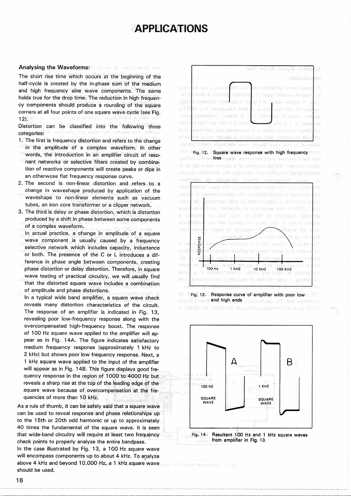
Analysing
theWaveforms:
The
shortrisetimewhichoccursatthebeginningofthe
half-cycle
iscreatedbythein-phasesumofthemedium
and
highfrequencysinewavecomponents.Thesame
holdstrueforthedroptime.Thereductioninhighfrequen-
cy
componentsshouldproducea roundingofthesquare
corners
atallfourpointsofonesquarewavecycle(seeFig.
12).
Distortioncanbeclassified
into
thefollowingthree
categories:
1.
Thefirstisfrequencydistortionandreferstothechange
intheamplitudeofa complexwaveform.Inother
words,
theintroductioninanamplifiercircuitof
reso-
nantnetworksorselectivefilterscreatedbycombina-
tion
ofreactivecomponentswillcreatepeaksordipsin
an
otherwoseflatfrequencyresponsecurve.
2.
Thesecondisnon-lineardistortionandreferstoa
change
inwaveshapeproducedbyapplicationofthe
waveshape
tonon-linearelementssuchasvacuum
tubes,
anironcoretransformerora clippernetwork.
3.
The
third
isdelayorphasedistortion,whichisdistortion
producedbya shiftinphasebetweensomecomponents
ofa complexwaveform.
Inactualpractice,a changeinamplitudeofa square
wave
componentisusuallycausedbya frequency
selective
networkwhichincludescapacity,inductance
orboth.ThepresenceoftheC orL introducesa
dif-
ference
inphaseanglebetweencomponents,creating
phase
distortionordelaydistortion.Therefore,insquare
wave
testingofpracticalcircuitry,wewillusually
find
thatthedistortedsquarewaveincludesa combination
ofamplitudeandphasedistortions.
Ina typicalwidebandamplifier,a squarewavecheck
reveals
manydistortioncharacteristicsofthecircuit.
The
responseofanamplifierisindicatedinFig.13,
revealing
poorlow-frequencyresponsealongwiththe
overcompensated
high-frequencyboost.Theresponse
of100Hzsquarewaveappliedtotheamplifierwillap-
pear
asinFig.14A.Thefigureindicatessatisfactory
mediumfrequencyresponse(approximately1 kHzto
2
kHz)butshowspoorlowfrequencyresponse.Next,a
1
kHzsquarewaveappliedtotheinputoftheamplifier
willappearasinFig.14B.
This
figuredisplaysgoodfre-
quency
responseintheregionof1000to4000Hzbut
reveals
a sharpriseatthetopoftheleadingedgeofthe
square
wavebecauseofovercompensationatthefre-
quencies
ofmorethan10kHz.
As
a ruleofthumb,itcanbesafelysaidthata squarewave
can
beusedtorevealresponseandphaserelationshipsup
tothe
1
5thor20thoddharmonicoruptoapproximately
40
timesthefundamentalofthesquare
wave.
Itis
seen
thatwide-bandcircuitrywillrequireatleasttwofrequency
check
pointstoproperlyanalyzetheentirebandpass.
Inthe
case
illustratedbyFig.13,a 100Hzsquarewave
willencompasscomponentsuptoabout4 kHz.Toanalyze
above
4 kHzandbeyond10,000Hz,a 1 kHzsquarewave
shouldbe
used.
Fig.
12.Squarewaveresponsewithhighfrequency
loss
Fig.
13.
Response
curveofamplifierwithpoorlow
and
highends
100HZ
SQUARE
WAVE
A
1
KHZ
SQUARE
WAVE
B
Fig.
14.Resultant100Hzand1 kHzsquarewaves
fromamplifierinFig.13.
16
RESPONSE

APPLICATIONS
Now,
the
regionbetween
100Hzand400HzinFig.13
shows
a
rise
from
poorlow-frequency(1000
Hzto1 kHz)
response
toa
flattening
out
from
beyond
1000and
4000
Hz.
Therefore,
<wecan
expectthat
the
higherfre-
quency
components
inthe100Hz
squarewavewill
be
relatively
normal
in
amplitude
and
phase
but
that
thelow-
frequency
components
"B" in
this
same
squarewavewill
be
modified
bythe
poorlow-frequencyresponse
of
this
amplifier(seeFig.
14A).
If
the
amplifierwere
such
asto
onlydepress
thelow
fre-
quency
components
inthe
square
wave,
a
curvesimilar
to
Fig.
15
would
be
obtained.However,reduction
in
amplitude
ofthe
components
is
ususally
caused
bya
reac-
tiveelement,
causing,
in
turn,
a
phaseshift
ofthe
com-
ponents,
producting
thetiltas
shown
in
Fig.
14A.
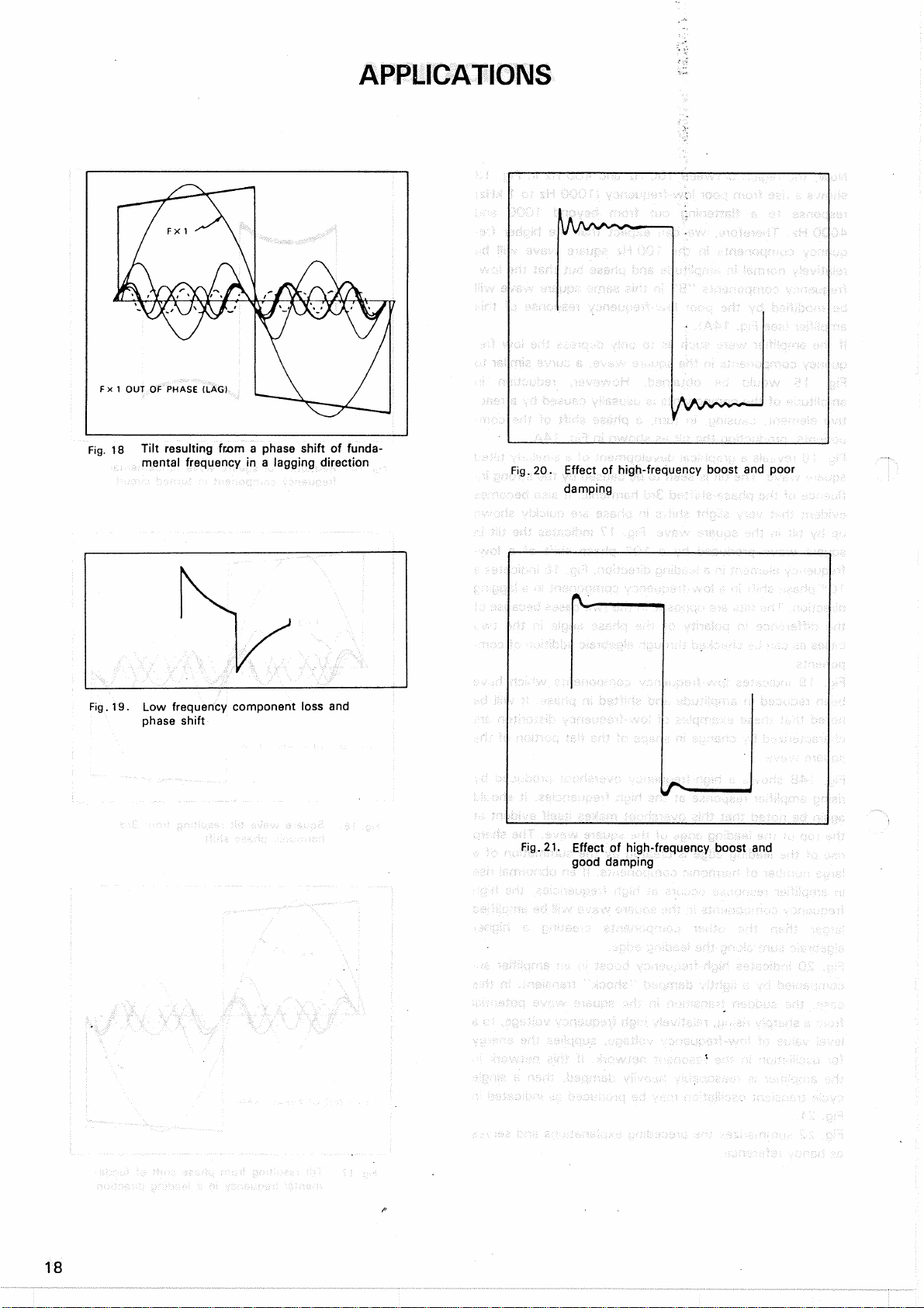
Fig.
16
reveals
a
graphicaldevelopment
ofa
similarly
tilted
square
wave.
The
tiltis
seen
tobe
caused
bythe
strong
in-
fluence
ofthe
phase-shifted
3rd
harmonic.
It
also
becomes
evidentthatveryslightshifts
in
phase
are
quicklyshown
up
bytiltinthe
square
wave.
Fig.17
indicates
thetiltin
square
waveproduced
bya 10°
phaseshift
ofa low-
frequency
element
ina
leadingdirection.Fig.
18
indicates
a
10°
phaseshift
ina
low-frequencycomponent
ina
lagging
direction.The
tilts
areopposite
inthetwo
cases
because
of
thedifference
in
polarity
ofthe
phaseangle
inthetwo
cases
as
can
be
checked
through
algebraic
addition
of
com-
ponents.
Fig.
19
indicateslow-frequencycomponentswhichhave
been
reduced
in
amplitude
and
shifted
in
phase.
It
will
be
notedthattheseexamples
of
low-frequency
distoriton
are
characterized
by
change
in
shape
ofthe
flat
portion
ofthe
square
wave.
Fig.
14B
shows
a
high-frequencyovershootproduced
by
rising
amplifierresponse
atthe
highfrequencies.
It
should
again
be
notedthatthisovershoot
makes
itselfevident
at
the
topofthe
leadingedge
ofthe
square
wave.
Thesharp
rise
ofthe
leadingedge
is
created
bythe
summation
ofa
large
number
of
harmoniccomponents.
Ifan
obnormal
rise
inamplifierresponseoccurs
at
highfrequencies,
the
high
frequency
components
inthe
squarewavewill
be
amplified
larger
than
the
othercomponentscreating
a
higher
algebraic
sum
along
the
leadingedge.
Fig.
20
indicateshigh-frequencyboost
inan
amplifier
ac-
companied
bya
lightly
damped"shock"transient.
In
this
case,
the
suddentransition
inthe
squarewavepotential
from
a
sharplyrising,relativelyhighfrequencyvoltage,
toa
level
value
of
low-frequencyvoltage,supplies
the
energy
foroscillation
inthe
resonantnetwork.
If
thisnetwork
in
theamplifier
is
reasonablyheavilydamped,then
a
single
cycle
transientoscillation
maybe
produced
as
indicated
in
Fig.
21.
Fig.
22
summarizes
the
precedingexplanations
and
serves
as
handyreference.
Fig.
15-
Reduction
of
squarewavefundamental
frequency
component
in
turnedcircuit
Fig.
16.
Squarewave
tilt
resultingfrom
3rd
harmonic
phase
shift
Fig.
17.
Tiltresultingfrom
phase
shift
of
funda-
mentalfrequency
ina
leadingdirection
17
F
x
3
F
x 3 OUTOF
PHASE
(LEAD)
F
x 1
F
X 1 OUTOF
PHASE
(LEAD)
APPLICATIONS
Fig.
19.Lowfrequencycomponent
loss
and
phase
shift
Fig.
21.Effectofhigh-frequencyboostand
gooddamping
F
x 1 OUTOF
PHASE
(LAG)
Fig.
18
Tilt
resulting
from
a
phase
shiftoffunda-
mental
frequencyina laggingdirection
Fig.
20.Effectofhigh-frequencyboostandpoor
damping
18
APPLICATIONS
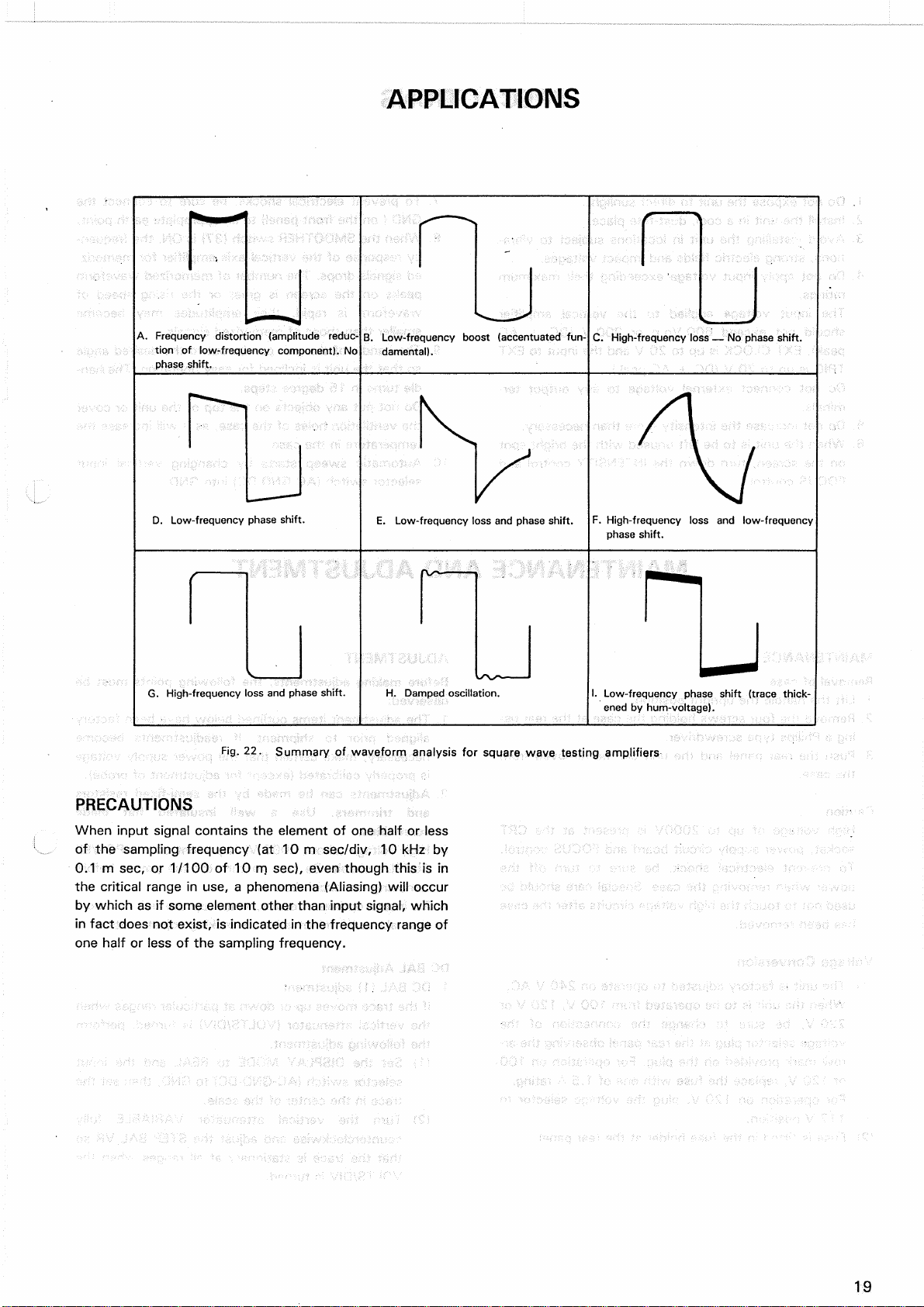
A.
Frequency
distortion
(amplitudereduc-
tion
oflow-frequencycomponent).No
phase
shift.
B.
Low-frequencyboost(accentuatedfun-
idamental).
C.
High-frequency
loss
— Nophaseshift.
D.Low-frequencyphaseshift.
E.
Low-frequency
loss
andphaseshift.
F.
High-frequency
loss
andlow-frequency
phase
shift.
G.
High-frequency
loss
andphaseshift.
H.
Dampedoscillation.
I.
Low-frequencyphaseshift(tracethick-
ened
byhum-voltage).
Fig.22.Summaryofwaveform
analysis
forsquarewavetestingamplifiers
PRECAUTIONS
When
input
signalcontainstheelementofonehalfor
less
ofthesamplingfrequency(at10m sec/div,10kHzby
0.1m sec,or1/100of10m sec),even
though
thisisin
thecriticalrangeinuse,a phenomena(Aliasing)
will
occur
bywhichasifsomeelementotherthan
input
signal,which
infactdoesnotexist,isindicatedinthefrequencyrangeof
onehalfor
less
ofthesamplingfrequency.
19
PRECAUTIONS
1.
Donotexposetheunittodirectsunlight.
2.
Installtheunitina cool,dust-freeplace.
3.
Avoidinstallingtheunitinlocationssubjecttovibra-
tions,strongelectricfieldsandimpactvoltages.
4.
Donotapplyinputvoltageexceedingtheirmaximum
ratings.
The
inputvoltageappliedtotheverticalamplifier
shouldnotexceed600Vp-por300V (DC+ AC
peak),
EXT
CLOCK
isupto20V andtheinputtoEXT
TRIG
isupto20V (DC+ AC
peak).
Donotconnectexternalvoltagetoany
output
ter-
minals.
5.
Donotincreasetheintensitymorethan
necessary.
6.
Whentheunitistobeleftunusedwiththe
bright
spot
onthe
screen,
turn
downthe
INTENSITY
controland
FOCUS
control.
7.
Topreventelectrical
shocks,
besuretoconnectthe
GND
( onthe
front
panel)toanappropiateearth
point.
8.
Whenthe
SMOOTHER
switch(37)isON,thefrequen-
cy
responseofthevertical
axis
amplifierformemoriz-
ed
signalsdrops.Thenumberofmemorizedwaveform
peaks
onthescreenisgreatortherisingspeedof
waveformisrapid,theiramplitudesmaybecome
smaller
thanthoseofmemorizedsignals.
9.
Thehandleoftheunitcanbesettothedesiredangle
so
thattheunitisinclinedfor
easy
operation.The
han-
dleturnsin
1
5 degree
steps.
Donotputanyobjectsonthetopoftheunitorcover
theventilationholesofthe
case,
asitwillincreasethe
temperatureinthe
case.
10.
Automaticsweepstartsbychangingverticalinput
selector
switch
(AC-GND-DC)
into
GND.
MAINTENANCE
ANDADJUSTMENT
MAINTENANCE
Removal
of
case
1.
Liftthehandletheuprightposition.
2.
Removethefour
screws
holdingthe
case
attherearus-
inga Philipstypescrewdriver.
3.
Push
therearpanelandtheunitcanberemovedfrom
the
case.
Caution
Highvoltageofupto2000VispresentattheCRT
socket,
powersupplycircuitboardand
FOCUS
control.
To
preventelectricalshock,besureto
turn
offthe
powerwhenremovingthe
case.
Special
careshouldbe
used
nottotouchthehighvoltagecircuitsafterthe
case
has
beenremoved.
VoltageConversion
(1)
Theunitisfactoryadjustedtooperateon240V AC.
When
theunitistobeoperatedfrom100V,120V or
220
V,besuretochangetheconnectionofthe
voltageselectorplugattherearpanelobservingthear-
rowmarkprovidedontheplug.Foroperationon100
or120V,replacethefusewithoneof1.5A rating.
For
operationon120V,plugthevoltageselectorto
117V
position.
(2)
Fuse
is
fitted
inthefuseholderattherearpanel.
ADJUSTMENT
Before
makingadjustments,thefollowingpointsmustbe
observed:
1.
Theadjustmentitemsoutlinedbelowhavebeenfactory
alignedpriortoshipment.Ifreadjustmentsbecome
necessary,
makecertainthatthepowersupplyvoltage
is
properlycalibrated(exceptforadjustmentofprobe).
2.
Adjustmentscanbemadebythesemi-fixed
resistors
and
trimmers.Usea wellinsulated
flat
blade
screwdriver.
3.
Highvoltage(about2000V)ispresentonthe
POWER
SUPPLY
circuit.Besureto
turn
offthepowerbefore
removingthecircuitboards.
4.
Toinsureoptimumresults,warmuptheunitformore
thanabout30minutesbeforemakingadjustments.
DC
BALAdjustment
1.
DCBAL(1)adjustment
Ifthetracemovesupordownatparticularrangeswhen
theverticalattenuator
(VOLTS/DIV)
isturned,perform
thefollowingadjustment.
(1)
Setthe
DISPLAY
MODEto
REAL
andtheinput
selector
switch
(AC-GND-DC)'to
GND,thensetthe
trace
inthecenterofthe
scale.
(2)
Turntheverticalattenuator
VARIABLE
fully
counterclockwise
andadjustthe
STEP
BALVRso
thatthetraceisstationaryatallrangeswhenthe
VOLTS/DIV
isturned.
20
Table of contents
Other Trio Test Equipment manuals


