Unicorn Computer ENDAT-3701 User manual

ENDAT-3701/3702
ENDAT-3902
All-In-One motherboard
User’s Manual
Rev. 5x
For 3701 PCB ver.3A or later
For 3702 PCB ver.4A or later
For 3902 PCB ver.4A or later
6/11/2004
II
The ENDAT-3701/3702/3902 All-In-One motherboard
Copyright Notice
The content of this manual has been checked for accuracy. The manufacturer
assumes no responsibility for any inaccuracies that may be contained in this
manual. The manufacturer reserves the right to make improvements or
modification to the this document and/or the product at any time without prior
notice. No part of this document may be reproduced, transmitted, photocopied or
translated into any language, in any form or by any means, electronic, mechanical,
magnetic, optical or chemical, without the prior written permission of the
manufacturer.
VIA is registered trademark of VIA Technology Incorporation
VT82C868A may only be used to identify products of VIA Technology
Realtek is registered trademark of Realtek Technologies Inc.
Multiscan is a trademark of Sony Corp of America
IBM, EGA, VGA, PC/XT, PC/AT, OS/2 and PS/2 are registered trademarks of
International Business Machines Corporation
Intel is a registered trademark of Intel Corporation
Plug and Play is registered trademarks of Intel Corporation
Microsoft, Windows and MS-DOS are trademarks of Microsoft Corporation
Award is a trademark of Award Software Inc.
PCI is a registered trademark of PCI Special Interest Group
Other product names mentioned herein are used for identification purpose only
and may be trademarks and/or registered trademarks of their respective
companies.
Installation Notice
The manufacturer recommends using a grounded plug to ensure proper
motherboard operation. Care should be used in proper conjunction with a
grounded power receptacle to avoid possible electrical shock. All integrated
circuits on this motherboard are sensitive to static electricity. To avoid damaging
components from electrostatic discharge, please do not remove the board from the
anti-static packing before discharging any static electricity to your body, by
wearing a wrist-grounding strap. The manufacturer is not responsible for any
damage to the motherboard due to improper operation.

User’s Manual III
Specification
:
This manual covers three different layout model of
PIII embedded motherboard. The respective board layout outlines are
shown on Chapter 1-4/1-5/1-6. Please refer to the following description to
make sure which model you have before using.
MODEL ENDAT-3701
/3701-030 ENDAT-3702 ENDAT-3902
CPU Socket370 Intel
®
Pentium
®
III FCPGA/Celeron™ Processor
System Chipset VIA PM133 VT8605 Chipset
System Bios Award (4Mbit Flash ROM)
VGA Adapter C&T69000/ 69030
Chipset
VIA Chipset Built-in S3 Savage4 AGP 4x
Graphic
LCD Feature Support TTL LCD TMDS Interface, via LCD kit (optional)
LAN Adapter Realtek 8139C 10BaseT/100BaseT Fast Ethernet
(Boot ROM Optional)
Flash Disk Socket for DiskOnChip 2000
System Memory Up to 1GB (PC66/PC100/PC133)
IDE Interface PCI IDE Support Ultra DMA33/66
I/O
Supports 4 Serial and 2 Parallel Ports
COM1, 2, 3, 4 with +5V/+12V Power
Supports RS422/485 for COM2 (Optional)
IRDA / USB Port Yes (Pin Header)
Audio Port (optional) Yes (via AV-CARD)
Expansion Slot Extension for PCI/ISA Bus
Location of Expansion
Slot At the 7
th
of Standard AT MB At the 6
th
of Standard
AT M B
Keyboard / Mouse Jack Two Mini Din Jack / Pin Header
Pin Header for I/O ports
(optional )
VGA / Multi I/O ports
AT / AT X P o w e r
Connector
Yes
Form Factor WD/LPX (220x220mm) PC/AT (223x220mm)

TABLE OF CONTENTS
CHAPTER 1. INTRODUCTION.................................................1
1-1. FEATURES............................................................................................. 1
1-2. UNPACKING ......................................................................................... 3
1-3. ELECTROSTATIC DISCHARGE PRECAUTIONS ............................. 3
1-4. MOTHERBOARD LAYOUT (ENDAT-3701)....................................... 4
1-5. MOTHERBOARD LAYOUT (ENDAT-3702)....................................... 5
1-6. MOTHERBOARD LAYOUT (ENDAT-3902) ...................................... 6
CHAPTER 2. SETTING UP THE MOTHERBOARD..............7
2-1. JUMPERS AND CONNECTORS (ENDAT-3701) ................................. 7
2-2. JUMPERS AND CONNECTORS (ENDAT-3702) .............................. 13
2-3. JUMPERS AND CONNECTORS (ENDAT-3902) .............................. 18
2-4. INSTALLING MEMORY ..................................................................... 23
2-5. SHARED VGA MEMORY ................................................................... 23
2-6. INSTALLING RISER CARD................................................................ 23
2-7. ASSIGNING IRQs FOR EXPANSION CARDS................................... 24
2-8. ASSIGNING DMA CHANNELS FOR ISA CARDS............................ 25
CHAPTER 3. AWARD BIOS SETUP........................................27
3-1. QUICK SETUP...................................................................................... 27
3-2. DESCRIPTION OF BIOS SETUP OPTIONS....................................... 28
3-3. ADVANCED BIOS FEATURES ........................................................... 28
3-4. ADVANCED CHIPSET FEATURES .................................................... 29
3-5. INTEGRATED PERIPHERALS .......................................................... 31
3-6. POWER MANAGEMENT SETUP....................................................... 33
3-7. PnP/PCI CONFIGURATIONS SETUP ................................................. 35
3-8. PC HEALTH STATUST ........................................................................ 36
CHPATER 4. VGA, LCD, DOC, IDE FEATURE ....................37
4-1. AGP-BUS VGA FEATURE................................................................... 37
VI
The ENDAT-3701/3702/3902 All-In-One motherboard
4-2. LCD FLAT PANEL FEATURE.............................................................. 38
4-3. PCI BUS AUDIO ADAPTER FEATURE.............................................. 40
4-4. DISKONCHIP FEATURE ..................................................................... 41
4-5. DRIVER UTILITY INSTALLATION GUIDE .....................................42
CHPATER 5. LAN ADAPTER...................................................45
5-1. FEATURES............................................................................................ 45
5-2. UTP CABLE/RJ-45 JACK DEFINITION .............................................46
5-3. CONNECTING 100BASE-TX FAST ETHERNET NETWORK.......... 47
5-4. CONNECTING 10BASE-T ETHERNET NETWORK......................... 47
5-5. 10M BASE/100MBASE INSTALLATION NOTICE............................ 47
5-6. REMOTE BOOT ROM INSTALLATION GUIDE ...............................48
5-7. LED INDICATORS ............................................................................... 49
5-8. SETUP PROGRAM .............................................................................. 49
5-9. LAN DRIVER INSTALLATION PROCEDURE .................................. 52
APPENDIX A: FLASH MEMORY UTILITY..........................53
APPENDIX B: CONNECTOR PIN ASSIGNMENT ...............55
APPENDIX C: LIMITED WARRANTY ..................................63

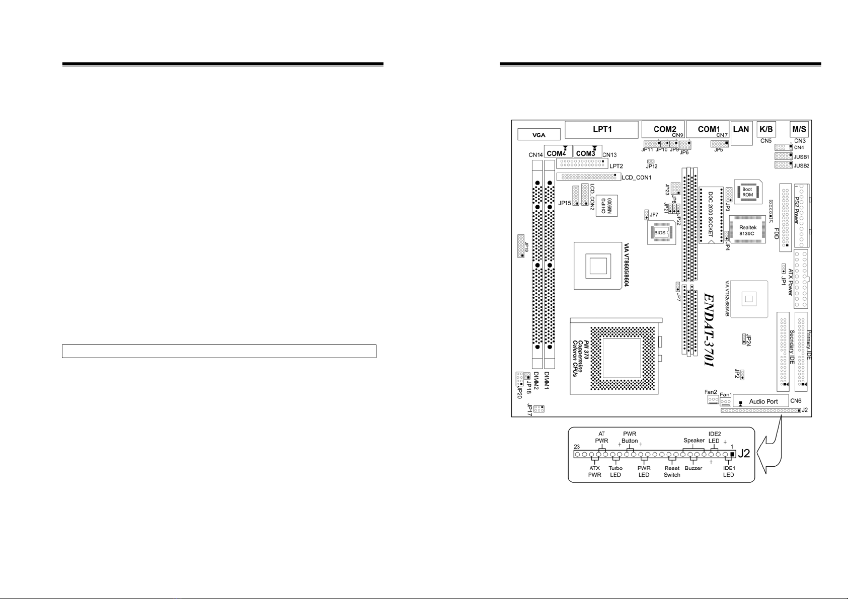
Chapter 1. Introduction
The ENDAT-3701, ENDAT-3702 and ENDAT-3902 All-In-One motherboard
uses VIA chipsets built-in VGA and Audio feature onboard, supports LCD feature
with TMDS interface via optional kit, built-in Realtek 8139xx LAN chipset with
RJ45 Jack for 10BaseT/100BaseT. This board offers the highest performance PC
specifications in the industry. The ENDAT-3701, ENDAT-3702 and
ENDAT-3902 runs with the Intel
®
Pentium
®
III FCPGA / Celeron™ Processor.
The motherboard is fully compatible with industry standards, adding many
technical enhancements and is fully compatible with thousands of software
applications developed for IBM PC/AT compatible computers. The control logic
provides high-speed performance for the most advanced multi-user, multitasking
applications available today. “Tomorrows PC technology is here today”.
1-1. Features
Basic Feature:
•
Supports all Socket-370 Processors Including Intel Pentium II, Pentium III,
VIA-Cyrix-III and Intel Coppermine / Celeron CPU; base on 66 / 100 /133 MHz
CPU “Front Side Bus (FSB)”.
•
High performance SMA North Bridge: Integrated VIA Apollo Pro133 and S3
Savage4 in a single chip, provides superior performance between the CPU, DRAM,
AGP bus, and PCI bus with pipelined, burst and concurrent operation.
•
Advance Memory Controller supporting PC100/PC133 SDRAM.
•
64-bit DRAM interface runs synchronous mode (66/66, 100/100, 133/133) or
pseudo-synchronous (66/100, 100/66, 100/133, 133/100) mode with FSB.
•
Supports up to 1GB of DRAM memory with 2 x 168 pin DIMM socket
•
Built-in C&T 69000 Chipset supports High Performance Flat Panel /
CRT HiQVideo with Integrated 2MB Memory (For ENADT-3701)
•
AGP controller supports 266Mhz 4x mode (For ENDAT-3702/3902)
•
Onboard built-in PCI BUS master IDE controller and one floppy drive controller.
2
The ENDAT-3701/3702/3902
All-In-One motherboard
•
PCI 2.2 compliant 32-bit PCI interface with 5V tolerant inputs.
•
Onboard socket DiskOnChip supports M-System products.
•
Onboard LAN Adapter supports 10BaseT/100BaseT,BOOT ROM optional (PLCC
Type), and LAN Features can be Enabled/Disabled by jumper settings.
•
Support 4 COM ports, STD.RI (RS-232), COM1, 2, 3, 4 with +5V/+12V DC
power selectable, with option of RS-422/485 features via COM2.
•
Support 2
Parallel Ports
•
Support Ultra DMA33/66 EIDE.
•
Onboard built-in 4 ports USB functions.
•
188 pin expansion slot for both PCI and ISA BUS signals.
•
IR function can be Enabled/Disabled by BIOS
Optional Features
•
Supports RS422/RS485 interface with COM2 (Optional)
•
For ENDAT-3702/3902, support Digital LCD Panel with 12bits digital signal for
TMDS LCD monitor
(via TMDS kit UC-TT1811)
•
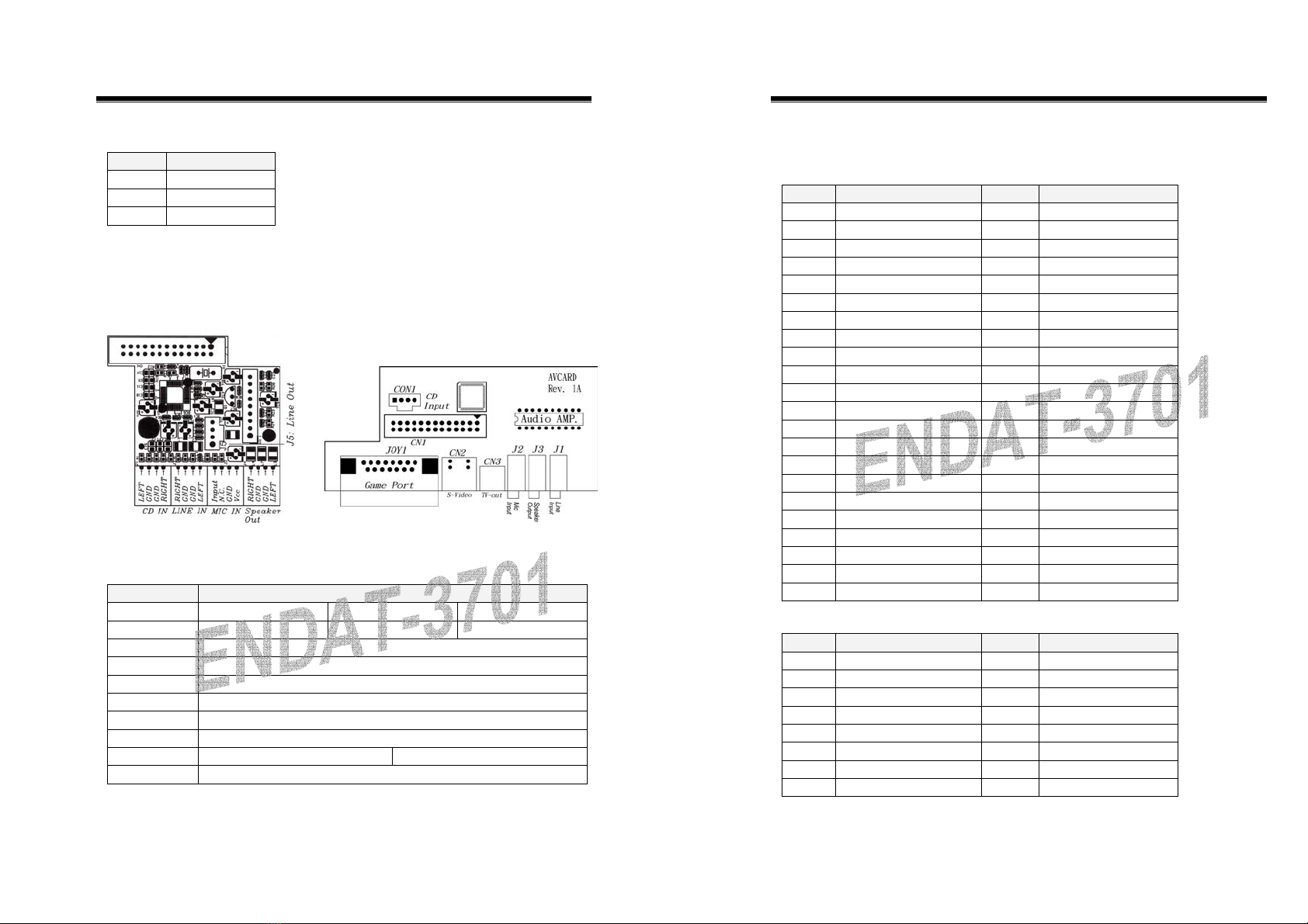
Supports Audio function
(via AV Card Kit)
•
Supports TV-Out feature
(via TV-Out adapter Kit)
Ordering information:
Digital TMDS adapter Kit for ENDAT-3702/3902 :Model No. UC-TT18xx
TTL Panel adapter Kit for ENDAT-3701: Model No. UC-LT1815
UC-LR
1815
UC-
T1848
UC-L
1836
UC-
L2448

User’s Manual 3
1-2. Unpacking
The motherboard comes securely packaged in a sturdy cardboard shipping carton.
In addition to the User's Manual, the motherboard package includes the following
items:
•
ENDAT-3701/ 3702/ 3902 All-In-One Motherboard
•
HDC/FDC Cables
•
TV-Out adapter / cable
(Optional)
•
Audio Kit
(Optional)
•
LCD kit
(Optional)
•
Serial port kit for 2 ports
•
IDE Driver includes: Drivers for Windows NT 3.x/4.x, Windows 95, 98,
2000, WinMe, Novell Netware and AWARD FLASH ROM utilities.
•
Driver utilities for on-board VGA drivers, LAN adapter and DOC 2000
If any of these items are missing or damage, please contact the dealer from whom
you purchase the motherboard. Save the shipping material and carton in the event
that you want to ship or store the board in the future.
Note:
Leave the motherboard in its original package until you are ready to install it!
1-3. Electrostatic Discharge Precautions
Make sure you properly ground yourself before handling the motherboard, or other
system components. Electrostatic discharge can easily damage the components.
Note: You must take special precaution when handling the motherboard in dry or
air-conditioned environments.
4
The ENDAT-3701/3702/3902
All-In-One motherboard
1-4. Motherboard Layout (ENDAT-3701)

User’s Manual 5
1-5. Motherboard Layout (ENDAT-3702)
6
The ENDAT-3701/3702/3902
All-In-One motherboard
1-6. Motherboard Layout (ENDAT-3902)

Chapter 2. Setting up the Motherboard
This chapter describes how to set up the motherboard and get ready for operation.
•
Installing the CPU upgrade
•
Installing DIMM memory. Make sure the correct CPU operating
voltage, jumper settings and frequency.
•
Double-check the insertion and orientation of the CPU before applying
power. Improper installation will result in permanent damage to the
CPU.
2-1. Jumpers and Connectors (ENDAT-3701)
Jumpers/Connectors Overview:
Function Jumpers/Connectors
CPU: CPU Clock Frequency JP18
CPU Type JP17(1-2,3-4,5-6), JP20(5-6,7-8)
Connector for Cooling Fan FAN1,FAN2
Power Supply: Type (ATX or PS/2) CN2(ATX);CN1(PS/2)
Power Good JP2
ATX or PS/2 AT Power Selector JP24; J2 Pin 19, 20, 21
ATX Power On/Off Switch J2 Pin 15, 16
Audio Output Port Connector CN6
LAN Adapter Disable/Enable JP4
On-Board VGA Disable/Enable JP21
PCI INT selector for Expansion Slot JP23
COM3 Port CN13
COM4 Port CN14
2
nd
Parallel Port
LPT2
COM Ports IRQ Setting BIOS Defined
COM Ports Power Selector (COM1, 2, 3,4) JP5, JP11
RS232/RS422/RS485 Selector (COM2) JP6, JP9, JP10, JP12
8
The ENDAT-3701/3702/3902
All-In-One motherboard
DiskOnChip Memory Address JP3
LCD Connector LCD_CON1; LCD_CON2
LCD Panel Type Selector JP15
Clear CMOS JP7
PS/2 Keyboard Jack CN5
PS/2 Mouse Jack CN3
PS/2 Mouse/KB Pin Header CN4
IR J1
USB Header JUSB1, JUSB2
FDD Connector FDD1
IDE 1 (Primary IDE) IDE1
IDE 2 (Secondary IDE) IDE2
Header for Case Panel J2
IDE 1 LED J2 Pin 1, Pin 2
IDE 2 LED J2 Pin 3, Pin 4
External Speaker J2 Pin 5, Pin 8
Buzzer On/Off J2 Pin 6, Pin 7
Hardware Reset Switch J2 Pin 9, Pin 10
Power LED J2 Pin 13, Pin 14
ATX Power Supply On/Off Switch J2 Pin 15, Pin 16
Turbo LED (for case only, no function) J2 Pin 17, Pin 18
ATX or PS/2 Power Selector J2 Pin 19, Pin 20, Pin 21
Ring-Detected J2 Pin 22, Pin 23
CPU Type Setting: JP17 / JP20
Jumper No.
CPU Type
JP17
(1-2)
JP17
(3-4)
JP17
(5-6)
JP20
(7-8)
JP20
(5-6)
Intel 0.25u Celeron
SHORT OPEN OPEN SHORT OPEN
Intel 0.18u
Celeron.
Coppermine
OPEN SHORT OPEN SHORT OPEN
Cyrix
SHORT OPEN SHORT OPEN SHORT
Note: CPU ratio already locked by CPU internally.

User’s Manual 9
System Clock Setting: JP18
JP18 (1-2) JP18 (3-4) CPU BUS CLOCK PCI CLOCK
OPEN OPEN 133 MHz 33.3 MHz
OPEN CLOSE 100 MHz 33.3 MHz
CLOSE CLOSE 66 MHz 33 MHz
Caution:
Please make sure the CPU type setting and System clock setting as
mention above for your system. Any wrong setting may cause
system damaged the CPU or system not working.
JP2: On-board Power Good Selector
Pin 1-2 Using External Power Good
Pin 2-3 * Using On Board Power Good
JP7: CMOS Data Clear:
Pin 1-2 * Normal
Pin 2-3 Clear CMOS Data
JP3: DiskOnChip Memory Address Selector
JP3 Memory Address
1-2 7-8
0C800H- 0C9FFH
1-2 9-10
0CC00H - 0CDFFH
3-4 7-8
0D000H- 0D1FFH
3-4 9-10
0D400H- 0D5FFH
5-6* 7-8* 0 D 8 0 0 H - 0 D 9 F F H
JP4: On-board LAN Disable/Enable
JP4 Function
Pin 1-2 * Enable On-Board LAN
Pin 2-3 Disable On-Board LAN
JP8 / JP22: Flash ROM Size/Voltage selector.
JP8 FLASH ROM SIZE
1-2=2MB *2-3=4MB
JP22 FLASH ROM Voltage
*1-2= 5V Type 2-3=3.3V Type
10
The ENDAT-3701/3702/3902
All-In-One motherboard
Box Header: COM1(CN7)/COM2(CN9)/COM3(CN13)/COM4(CN14)
Pin No. Description Pin No. Description
1 DCD 6 DSR
2 RXD 7 RTS
3 TXD 8 CTS
4 DTR 9 RI / PWR
5 GND 10 N.C.
JP5 : Voltage selector for COM1, COM2
COM1 COM2 Description
JP5 Close 1-2 Close 7-8 +5V
JP5 Close 3-4 Close 9-10 STD. RI. (RS-232)
JP5 Close 5-6 Close 11-12 +12V
JP11 : Voltage selector for COM3, COM4
COM3 COM4 Description
JP11 Close 1-2 Close 7-8 +12V
JP11 Close 3-4 Close 9-10 STD. RI. (RS-232)
JP11 Close 5-6 Close 11-12 +5V
JP10, JP12, JP6: RS232 / 485 Selector for COM2 Only.
TYPE JP10 JP12 JP6
RS-232 * 1-2 Open 1-2, 4-5, 7-8, 10-11
RS-485 3-4 Close 2-3, 5-6, 8-9, 11-12
* Make sure the port mode is set up correctly before installing any
peripherals.
JP21: On-board VGA Disable/Enable
Function Close
Disable Pin 1-2
Enable Pin 2-3 *
JP24 / J2’Pin 19~21: Power Supply Type
Power Type JP24 J2’s Pin 19~21
PS/2 AT Close 1-2 Close 19-20
ATX Close 2-3 Close 20-21
J2’s Pin15;16: For ATX Power Supply On/Off
Pin 15; Pin 16 On/Off Switch for ATX Power Button

User’s Manual 11
FAN1, FAN2: CPU / 2nd Cooling Fan Connector
Pin No. Function
Pin 1 Sensor Pin.
Pin 2 +12V
Pin 3 GND
CN6: Audio Output Port connector via AV Card Kit (Optional)
The AV Card Kit Adapter supports Sound and Game Port. Please
close pin13-14 to disable onboard Audio features if the AV Card Kit
is not inserted onto the CN6 connector.
UC-A001 AV Card
J2: Case Panel connection
Pin No. Description
1, 2 IDE 1 LED Pin 1 = – Pin 2 = +
3, 4 IDE 2 LED Pin 3 = – Pin 4 = +
5, 8 External Speaker
6, 7 Onboard Buzzer
9, 10 Reset Switch
13,14 Power LED Indicator
15, 16 Power On/Off Switch (for ATX Power only)
17, 18 Turbo LED(for case only, no function)
19, 20, 21 19-20 for PS/2 AT Power 20-21 for ATX Power
22, 23 Modem Ring Detected / Wake on LAN
Modem Ring/ Wake-On-LAN: WOL1, WOL2
12
The ENDAT-3701/3702/3902
All-In-One motherboard
LCD_CON1 / LCD_CON2: LCD PANEL OUTPUT Connector.
LCD_CON1: LCD Control signal & Data Bit 0 – Bit23
Pin No. Description Pin No. Description
1 VBL 2 VBL
3 GND 4 GND
5 LCDVSEL 6 LCDVSEL
7 ENAVEE 8 GND
9 PANEL DATA 0 10 PANEL DATA 1
11 PANEL DATA 2 12 PANEL DATA 3
13 PANEL DATA 4 14 PANEL DATA 5
15 PANEL DATA 6 16 PANEL DATA 7
17 PANEL DATA 8 18 PANEL DATA 9
19 PANEL DATA 10 20 PANEL DATA 11
21 PANEL DATA 12 22 PANEL DATA 13
23 PANEL DATA 14 24 PANEL DATA 15
25 PANEL DATA 16 26 PANEL DATA 17
27 PANEL DATA 18 28 PANEL DATA 19
29 PANEL DATA 20 30 PANEL DATA 21
31 PANEL DATA 22 32 PANEL DATA 23
33 GND 34 GND
35 SHFCLK 36 FLM
37 M-DE 38 LP
39 GND 40 CENABKL
41 NC 42 NC
43 VCC(+5V) 44 VCC(+5V)
LCD_CON2: LCD Data Bit 24 – Bit35
Pin No. Description Pin No. Description
1 LCDVSEL 2 VCC(+5V)
3 PANEL DATA 24 4 PANEL DATA 25
5 PANEL DATA 26 6 PANEL DATA 27
7 PANEL DATA 28 8 PANEL DATA 29
9 PANEL DATA 30 10 PANEL DATA 31
11 PANEL DATA 32 12 PANEL DATA 33
13 PANEL DATA 34 14 PANEL DATA 35
15 GND 16 GND

User’s Manual 13
2-2. Jumpers and Connectors (ENDAT-3702)
Jumpers/Connectors Overview:
Function Jumpers/Connectors
CPU: CPU Clock Frequency JP18
CPU Type JP17(1-2,3-4,5-6), JP20(5-6,7-8)
Connector for Cooling Fan FAN1,FAN2
Power Supply: Type (ATX or PS/2) CN2(ATX);CN1(PS/2)
Power Good JP2
ATX or PS/2 Power Selector JP24; J2 Pin 19, 20, 21
ATX Power On/Off Switch J2 Pin 15, 16
Audio Output Port Connector CN6
LAN Adapter Disable/Enable JP4
PCI INT selector for Expansion Slot JP23
COM3 Port CN13
COM4 Port CN14
2
nd
Parallel Port
LPT2
COM Ports IRQ Setting BIOS Defined
COM Ports Power Selector (COM1, 2, 3,4) COM 1/2=JP5, COM3/4= JP11
RS232/RS422/RS485 Selector (COM2) JP6, JP9, JP10, JP12
DiskOnChip Memory Address JP3
LCD Connector LCDTV1
Clear CMOS JP7
PS/2 Keyboard Jack CN5
PS/2 Mouse Jack CN3
PS/2 Mouse/KB Pin Header CN4
IR J1
USB Header JUSB1, JUSB2
FDD Connector FDD1
IDE 1 (Primary IDE) IDE1
IDE 2 (Secondary IDE) IDE2
14
The ENDAT-3701/3702/3902
All-In-One motherboard
Header for Case Panel J2
IDE 1 LED J2 Pin 1, Pin 2
IDE 2 LED J2 Pin 3, Pin 4
External Speaker J2 Pin 5, Pin 8
Buzzer On/Off J2 Pin 6, Pin 7
Hardware Reset Switch J2 Pin 9, Pin 10
Power LED J2 Pin 13, Pin 14
ATX Power Supply On/Off Switch J2 Pin 15, Pin 16
Turbo LED (for case only, no function) J2 Pin 17, Pin 18
ATX or PS/2 Power Selector J2 Pin 19, Pin 20, Pin 21
Ring-Detected J2 Pin 22, Pin 23
CPU Type Setting: JP17 / JP20
Jumper No.
CPU Type
JP17
(1-2)
JP17
(3-4)
JP17
(5-6)
JP20
(7-8)
JP20
(5-6)
Intel 0.25u
Celeron
SHORT OPEN OPEN SHORT OPEN
Intel 0.18u
Celeron.
Coppermine
OPEN SHORT OPEN SHORT OPEN
VIA/ Cyrix
SHORT OPEN SHORT OPEN SHORT
Note: CPU ratio already locked by CPU internally.
System Clock Setting: JP18
JP18 (1-2) JP18 (3-4) CPU CLOCK (FSB) PCI CLOCK
OPEN OPEN 133 MHz 33.3 MHz
OPEN CLOSE 100 MHz 33.3 MHz
CLOSE CLOSE 66 MHz 33 MHz
Caution:
Please make sure the CPU type setting and System clock setting as
mention above for your system. Any wrong setting may cause
system damaged the CPU or system not working.
JP2: On-board Power Good Selector
Pin 1-2 Using External Power Good
Pin 2-3 * Using On Board Power Good

User’s Manual 15
JP7: CMOS Data Clear:
Pin 1-2 * Normal
Pin 2-3 Clear CMOS Data
JP3: DiskOnChip Memory Address Selector
JP3 Memory Address
1-2 7-8
0C800H- 0C9FFH
1-2 9-10
0CC00H - 0CDFFH
3-4 7-8
0D000H- 0D1FFH
3-4 9-10
0D400H- 0D5FFH
*5-6 *7-8 0D800H- 0D9FFH
JP4: On-board LAN Disable/Enable
JP4 Function
Pin 1-2 * Enable On-Board LAN
Pin 2-3 Disable On-Board LAN
Box Header: COM1(CN7)/COM2(CN9)/COM3(CN13)/COM4(CN14)
Pin No. Description Pin No. Description
1 DCD 6 DSR
2 RXD 7 RTS
3 TXD 8 CTS
4 DTR 9 RI / PWR
5 GND 10 N.C.
JP5 : Voltage selector for COM1, COM2
COM1 COM2 Description
JP5 Close 1-2 Close 7-8 +5V
JP5 Close 3-4 Close 9-10 STD. RI. (RS-232)
JP5 Close 5-6 Close 11-12 +12V
JP11 : Voltage selector for COM3, COM4
COM3 COM4 Description
JP11 Close 1-2 Close 7-8 +12V
JP11 Close 3-4 Close 9-10 STD. RI. (RS-232)
JP11 Close 5-6 Close 11-12 +5V
16
The ENDAT-3701/3702/3902
All-In-One motherboard
JP10, JP12, JP6: RS232 / 485 Selector for COM2
TYPE JP10 JP12 JP6
RS-232 * 1-2 Open 1-2, 4-5, 7-8, 10-11
RS-485 3-4 Close 2-3, 5-6, 8-9, 11-12
* Make sure the port mode is set up correctly before installing any
peripherals.
JP8 / JP22: Flash ROM Size/Voltage selector.
JP8 FLASH ROM SIZE
1-2=2MB *2-3=4MB
JP22 FLASH ROM Voltage
1-2= 5V Type *2-3=3.3V Type
JP24 / J2’s Pin 19~21: Power Supply Type
Power Type JP24 J2’s Pin 19~21
PS/2 AT Close 1-2 Close 19-20
ATX Close 2-3 Close 20-21
J2’s Pin15;16: For ATX Power Supply On/Off
Pin 15; Pin 16 On/Off Switch for ATX Power Button
FAN1, FAN2: CPU / 2nd Cooling Fan Connector
Pin No. Function
Pin 1 Sensor Pin.
Pin 2 +12V
Pin 3 GND

User’s Manual 17
CN6: Audio Output Port connector via AV Card Kit (Optional)
The AV Card Kit Adapter supports Sound and Game Port. Please
close pin13-14 to disable onboard Audio features if the AV Card Kit
is not inserted onto the CN6 connector.
UC-A001 AV Card
J2: Case Panel connection
Pin No. Description
1, 2 IDE 1 LED Pin 1 = – Pin 2 = +
3, 4 IDE 2 LED Pin 3 = – Pin 4 = +
5, 8 External Speaker
6, 7 Onboard Buzzer
9, 10 Reset Switch
13,14 Power LED Indicator
15, 16 Power On/Off Switch (for ATX Power only)
17, 18 Turbo LED(for case only, no function)
19, 20, 21 19-20 for AT Power 20-21 for ATX Power
22, 23 Modem Ring Detected / Wake on LAN
18
The ENDAT-3701/3702/3902
All-In-One motherboard
2-3. Jumpers and Connectors (ENDAT-3902)
Jumpers/Connectors Overview (ENDAT-3902):
Function Jumpers/Connectors
CPU: CPU Clock Frequency JP17
CPU Type JP18, JP19
Connector for Cooling Fan FAN1,FAN2
Power Supply: Type (ATX or PS/2) CN2(ATX);CN1(PS/2)
Power Good JP3
ATX or PS/2 Power Selector JP24; J2 Pin 19, 20, 21
ATX Power On/Off Switch J2 Pin 15, 16
Audio Output Port Connector CN6
LAN Adapter Disable/Enable JP8
PCI INT selector for Expansion Slot JP23
COM2 Port CN7
COM3 Port CN12
COM4 Port CN11
2
nd
Parallel Port
LPT2
COM Ports IRQ Setting BIOS Defined
COM Ports Power Selector (COM1, 2, 3,4) COM1/2=JP1, COM3/4= JP13
RS232/RS422/RS485 Selector (COM2) JP6, JP7, JP4, JP5
DiskOnChip Memory Address JP11
LCD Connector (Optional) LCDTV1
Clear CMOS JP10
PS/2 Keyboard Jack CN3
PS/2 Mouse Jack CN5
PS/2 Mouse/KB Pin Header CN4
IR J1
USB Port Header JUSB1, JUSB2
FDD Connector FDD1
IDE 1(Primary IDE) IDE1
IDE 2 (Secondary IDE) IDE2

User’s Manual 19
Header for Case Panel J2
IDE 1 LED J2 Pin 1, Pin 2
IDE 2 LED J2 Pin 3, Pin 4
External Speaker J2 Pin 5, Pin 8
Buzzer On/Off J2 Pin 6, Pin 7
Hardware Reset Switch J2 Pin 9, Pin 10
Power LED J2 Pin 13, Pin 14
ATX Power Supply On/Off Switch J2 Pin 15, Pin 16
Turbo LED (for case only, no function) J2 Pin 17, Pin 18
ATX or PS/2 Power Selector J2 Pin 19, Pin 20, Pin 21
Ring-Detected J2 Pin 22, Pin 23
CPU Type Setting: JP19 / JP18
JUMPER No.
CPU Type
JP19
(1-2)
JP19
(3-4)
JP19
(5-6)
JP18
(7-8)
JP18
(5-6)
Intel 0.25u
Celeron SHORT OPEN OPEN SHORT OPEN
Intel 0.18u
Celeron
Coppermine
OPEN SHORT OPEN SHORT OPEN
VIA / Cyrix SHORT OPEN SHORT OPEN SHORT
Note: CPU ratio already locked by CPU internally.
System Clock Setting: JP17
JP17 (1-2) JP17 (3-4) CPU BUS
CLOCK
PCI BUS CLOCK
OPEN OPEN 133 MHz 33.3 MHz
OPEN CLOSE 100 MHz 33.3 MHz
CLOSE CLOSE 66 MHz 33 MHz
Caution:
Please make sure the CPU type setting and System clock setting as
mention above for your system. Any wrong setting may cause
system damaged the CPU or system not working.
20
The ENDAT-3701/3702/3902
All-In-One motherboard
JP10: CMOS Data Clear:
Pin 1-2 * Normal
Pin 2-3 Clear CMOS Data
JP11: DiskOnChip Memory Address Selector
JP11 Memory Address
1-2 7-8
0C800H - 0C9FFH
1-2 9-10
0CC00H - 0CDFFH
3-4 7-8
0D000H - 0D1FFH
3-4 9-10
0D400H - 0D5FFH
*5-6 *7-8 0D800H - 0D9FFH
JP8: On-board LAN Disable/Enable
Pin 1-2 * Enable On-Board LAN
Pin 2-3 Disable On-Board LAN
JP12 / JP22: Flash ROM Size/Voltage selector.
JP12 FLASH ROM SIZE
1-2=2MB *2-3=4MB
JP22 FLASH ROM Voltage
1-2= 5V Type *2-3=3.3V Type
Box Header: COM1(CN9)/COM2(CN7)/COM3(CN11)/COM4(CN12)
Pin No. Description Pin No. Description
1 DCD 6 DSR
2 RXD 7 RTS
3 TXD 8 CTS
4 DTR 9 RI / PWR
5 GND 10 N.C.
JP1: Voltage selector for COM1, COM2
COM1 COM2 Description
JP1 Close 1-2 Close 7-8 +5V
JP1 Close 3-4 Close 9-10 STD. RI. (RS-232)
JP1 Close 5-6 Close 11-12 +12V

User’s Manual 21
JP13: Voltage selector for COM3, COM4
COM3 COM4 Description
JP13 Close 1-2 Close 7-8 +12V
JP13 Close 3-4 Close 9-10 STD. RI. (RS-232)
JP13 Close 5-6 Close 11-12 +5V
JP6, JP7, JP4: RS232 / 485 Selector for COM2
TYPE JP6 JP7 JP4
RS-232 * 1-2 Open 1-2, 4-5, 7-8, 10-11
RS-485 3-4 Close 2-3, 5-6, 8-9, 11-12
*
Make sure the port mode is set up correctly before installing any
peripherals.
JP3: On-board Power Good Selector
JP3 Function
Pin 1-2 Using External Power Good
Pin 2-3 * Using On Board Power Good
FAN1, FAN2: CPU / 2nd Cooling Fan Connector
Pin No. Function
Pin 1 Sensor Pin.
Pin 2 +12V
Pin 3 GND
JP24; J2’s Pin 19~21: Power Supply Type
Power Type JP24 J2’s Pin 19~21
PS/2 AT Close 2-3 Close 19-20
ATX Close 1-2 Close 20-21
J2’s Pin15,16: For ATX Power Supply On/Off
Pin 15; Pin 16 On/Off Switch for ATX Power Button
22
The ENDAT-3701/3702/3902
All-In-One motherboard
CN6: Audio Output Port connector via AV Card Kit (Optional)
The AV Card Kit Adapter supports Sound, Game Port. Please close
pin13-14 to disable onboard Audio features if the AV Card Kit is not
inserted onto the CN6 connector.
UC-A001 AV Card
J2: Case Panel connection
Pin No. Description
1, 2 IDE 1 LED Pin 1 = –Pin 2 = +
3, 4 IDE 2 LED Pin 3 = –Pin 4 = +
5, 8 External Speaker
6, 7 Onboard Buzzer
9, 10 Reset Switch
13,14 Power LED Indicator
15, 16 Power On/Off Switch (for ATX Power only)
17, 18 Turbo LED(for case only, no function)
19, 20, 21 19-20 for AT Power 20-21 for ATX Power
22, 23 Modem Ring Detected / Wake on LAN

User’s Manual 23
2-4. Installing Memory
The motherboard offers two 168pin DIMM sockets supporting up to 1GB of
memory. The DIMM memory can be 66MHz, 100MHz (PC-100) or 133 MHz
(PC-133).
2-5. Shared VGA Memory
The ENDAT-3702 / ENDAT-3902 is using built-in AGP VGA controller with share
memory architecture (SMA) -
AGP mode with 2MB to 32MB
of system memory.
The ENDAT-3701 motherboard has 2MB build-in dedicate memory for VGA chip
C&T 69000, and 4MB build-in dedicated memory for chip C&T 69030. The
amount of video memory on motherboard determines the number of colors and the
video graphic resolution.
2-6. Installing Riser Card
Installing Riser Card (Max. 3 PCI Slot on Riser Card)
PCI Slot INT ADSEL
PCI 1 A,B,C,D AD24(Onboard LAN)
PCI 2 B,C,D,A AD23
PCI 3 C,D,A,B AD22
PCI 4 D,A,B,C AD21
There are two different riser cards that can be fitted to ENDAT-3701/3702/3902
All-In-One motherboard. The first one is a 98pin ISA only Bus riser card
(traditional ISA Bus riser card), the second one is a 188pins PCI/ISA riser card.
Please note: PCI/ISA riser cards jumper settings have to be matched
with the motherboard INT/AD-select jumper.
The default INT/AD-select
for ENDAT-3701/3702/3902 All-In-One motherboard is listed in the above table.
However, it could be revised by changing
JP23
setting for different INT/AD-select.
The following table shows the JP23 configurations:
24
The ENDAT-3701/3702/3902
All-In-One motherboard
JP23 Configurations:
Expansion for PCI Slot * JP23 = 1-2 JP23 = 2-3
Expansion PCI 1 INT =A,B,C,D INT = B,C,D,A
Expansion PCI 2 INT = B,C,D,A INT = C,D,A,B
Expansion PCI 3 INT = C,D,A,B INT = D,A,B,C
Expansion PCI 4 INT = D,A,B,C INT = A,B,C,D
Note: Even change the JP23 setting for different configuration the AD-select should
be match to each INT. Please using the default setting as above if you are not
familiar with the configuration of raiser card and add-on card .
Caution:
Do not insert PCI Bus Add-On cards directly into the on-board
expansion slot!
2-7. Assigning IRQs for Expansion Cards
Some expansion cards require an IRQ (Interrupt request vector) to operate.
Generally, each IRQ must be exclusively assigned to specific use. In a standard
design, there are 16 IRQ available with 11 of them already in used by other part of
the system.
Both ISA and PCI expansion cards may need to use IRQ. Cards installed in the ISA
Expansion Bus have the first priority to use the available system IRQs. Any
remaining IRQ then, may be assigned to this PCI Bus. Microsoft's Diagnostic
(MSD.EXE) utility included in the Windows directory can be used to see their map.
Make sure that there are no two devices using the same IRQ in the system.
Otherwise this will cause the system to hang up or give unexpected results. To
simplify the process, this motherboard complies with the Plug and Play (PnP)
specifications, which was developed to allow automatic system configuration.
Whenever a PnP-compliant card is added to the system, PnP cards and IRQs are
automatically assigned if available. If the system has both Legacy and PnP ISA
cards installed. IRQs are assigned to PnP cards from those not used by Legacy
cards. The PCI and PnP configuration in the BIOS setup utility can be used to
indicate which IRQs have being used by Legacy cards. For older Legacy cards that
do not work with the BIOS, you can contact your vendor for an ISA configuration
utility.

User’s Manual 25
An IRQ number is automatically assigned to PCI expansion cards after those used
by Legacy and PnP ISA cards. In the PCI Bus design, the BIOS is automatically
assigned an IRQ to a PCI slot that has a card in it which requires an IRQ. To install
a PCI card, you need to set the correct "ADSEL" and "INT" (interrupt) assignment.
Please refer to "Chapter 2-5" Installing a Riser Card for detail assignments.
IRQ Status Assignment
0 Used Timer
1 Used Keyboard
2 Used Second 8259
3 Used COM2
4 Used COM1
5 Used COM3
6 Used Floppy Disk
7 Used LPT1
8 Used RTC
9 Used LPT2
10 Used COM4
11 Used LAN Adapter (on board)
12 Used PS/2 Mouse
13 Used Coprocessor
14 Used Hard Disk (IDE 1)
15 Used Reserved (IDE 2)
2-8. Assigning DMA Channels for ISA Cards
Since ISA cards, both Legacy and PnP may also need to use a DMA (direct
memory access) channel, DMA assignments for this motherboard are
handled the same way as the IRQ assignment process described above. You
can select a DMA channel in the PCI and PnP configuration section of the
BIOS setup utility. In the BIOS setup, you should choose "Yes" for those
IRQ's and DMA's you wish to reserve for Legacy cards.

Chapter 3. AWARD BIOS SETUP
Use the CMOS setup program to modify the system parameters to reflect the
environment installed in your system and to customize the system as desired. Press
the <DEL> key to enter into the CMOS setup program when you turn on the power.
Settings can be accessed via arrow keys. Press <Enter> to choose an option to
configure the system properly.
In the main menu, press F10 or “SAVE & EXIT SETUP” to save your changes and
reboot the system. Choose “EXIT WITHOUT SAVING” to ignore the changes and
exit the setup procedure. Pressing <ESC> at anywhere during the setup will return
to the main menu.
“Advanced BIOS Features”, “Advanced Chipset Features” and “PnP/PCI
Configurations” requires board knowledge on PC/AT system architecture and VIA
chipset specification. They intend to be used by well-trained technicians and
experienced users. Incorrect setup could cause system malfunctions.
3-1. Quick Setup
In most cases, you can quickly configure the system by using the following
procedure. The manufacturer highly recommends that you use “Quick Setup” for
setting CMOS to avoid any unpredictable results.
1.
Choose “Standard CMOS Features” from the main menu, to configure the date
and time, hard disk type, floppy disk drive type etc.
2.
Choose “Load Optimized Defaults” from the menu for loading the defaults
parameters that is set by the manufacturer for the most stable normal
configuration.
3.
Press F10 or “SAVE & EXIT SETUP” to save the changes and reboot the
system.
28
The ENDAT-3701/3702/3902
All-In-One motherboard
3-2. Description of the BIOS Setup Option
Please make clear the means of those option parameters. Improper settings will
cause the system to hang up or perform poorly. Most items are clearly understood
from the screen prompt or “Help” by function key “F1”. The manufacturer highly
recommends that “Default” settings have been used to avoid any unpredictable
results.
3-3. Advanced BIOS Features Setup
Advanced
BIOS Features
Virus Warning : Disabled
CPU Internal Cache : Enabled
External Cache : Enabled
CPU L2 Cache ECC Checking : Enabled
Quick Power On Self Test : Enabled
First Boot Device : Floppy
Second Boot Device : HDD-0
Third Boot Device : LS120
Other Boot Device : Enabled
Swap Floppy Drive : Disabled
Boot Up Floppy Seek : Disabled
Boot Up NumLock Status : On
Gate A20 Option : Normal
Typematic Rate Setting : Disabled
Typematic Rate (Chars/Sec) : 6
Typematic Delay (Msec) : 250
Security Option : Setup
OS Select For DRAM > 64MB : Non-OS2
Video BIOS Shadow : Enabled
C8000-CBFFF Shadow : Disabled
CC000-CFFFF Shadow : Disabled
D0000-D3FFF Shadow : Disabled
D4000-D7FFF Shadow : Disabled
D8000-DBFFF Shadow : Disabled
DC000-DFFFF Shadow : Disabled

User’s Manual 29
3-4. Details of the Advanced Chipset Features Setup
Advanced Chipset Feature
DRAM Timing By SPD : Enabled
DRAM Clock : Host CLK
SDRAM Cycle Length : 3
Bank Interleave : Disabled
Memory Hole : Disabled
P2C/C2P Concurrency : Enabled
Fast R-W Turn Around :Disabled
System BIOS Cacheable : Enabled
Video BIOS Cacheable : Enabled
Frame Buffer Size : 8M
AGPAperture Size : 128M
AGP-4X Mode :Enabled
AGP Driving Control :Auto
OnChip USB : Disabled
CPU to PCI Write Buffer :Enabled
PCI Dynamic Bursting :Enabled
PCI Master 0 WS Write :Enabled
PCI Delay Transaction :Disabled
PCI#2 Access #1 Retry :Enabled
AGP Master 1 WS Write :Disabled
AGP Master 1 WS Read :Disabled
SDRAM Cycle Length
This item sets the CAS latency timing.
Video BIOS Cacheable
When enabled, the Video BIOS cache will cause access to video BIOS addressed at
C0000H to C7FFFH to be cached, if the cache controller is also enabled.
System BIOS Cacheable
Enabling this selection allows access to the system BIOS ROM addressed
F0000H-FFFFFH to be cached, provided the cache controller is enabled.
Memory Hole At 15Mb Addr.
In order to improve performance, certain space in memory is reserved for ISA cards.
This memory must be mapped into the memory space below 16MB.
Frame Buffer Size
Allocate the share memory size from system memory for Video
30
The ENDAT-3701/3702/3902
All-In-One motherboard
AGP Aperture Size
Selecting the size of Accelerated Graphics Port (AGP) aperture. The Aperture is a
portion of the PCI memory address range dedicated for graphics memory address
space. Host cycles that hit the aperture range are forwarded to the AGP without
any translation. See www.apgforum.org for AGP information.
OnChip USB
Select “Enabled” if your system contains a Universal Serial Bus (USB) controller
and you have a USB peripheral.
The “Assign IRQ for USB” has to be set to
Enabled on “PnP/PCI Configuration” (when the USB be used.)
CPU to PCI Write Buffer
When enabled, up to four D words of data can be written to the PCI bus without
interrupting the CPU. When disabled, a write buffer is not used and the CPU read
cycle will not be completed until the PCI bus signals is ready to receive the data.
PCI Delay Transaction
The chipset has an embedded 32-bit posted write buffer to support delay
transaction cycles. Select Enabled to support compliance with PCI specification
version 2.2.

User’s Manual 31
3-5. Integrated Peripherals
Integrated Peripherals
OnChip IDE Channel 0 : Enabled
OnChip IDE Channel 1 : Enabled
Primary Master PIO : Auto
Primary Slave PIO : Auto
Secondary master PIO : Auto
Secondary Slave PIO : Auto
Primary Master UDMA : Auto
Primary Slave UDMA : Auto
Secondary Master UDMA : Auto
Secondary Slave UDMA : Auto
InitDisplay First :PCI Slot
HDD Block Mode : Enabled
Onboard FDD Controller : Enabled
Onboard Serial Port 1 : 3F8/IRQ4
Onboard Serial Port 2 : 2F8/IRQ3
UART 2 Mode : Standard
Onboard Parallel Port : 378/IRQ7
Onboard Parallel Mode : ECP
ECP Mode use DMA : 3
Onboard serial Port 3 :3E8H
Serial Port 3 Use IRQ :IRQ5
Onboard serial Port 4 :2E8H
Serial Port 4 Use IRQ :IRQ10
Onboard Parallel Port 2 : 278H
Parallel Port 2 Use IRQ :IRQ9
Parallel Port 2 Mode :Normal
OnChip IDE Channel
This chipset contains a PCI IDE interface with support for two IDE channels.
Select Enabled to activate the first and/or second IDE interface. Select Disabled to
deactivate this interface, if a first and/or second add-in IDE interface is installed.
IDE Prefetch Mode
Enable pre-fetch for IDE drive interface that supports its faster drive access. If disk
drive errors appear, change the setting to omit the drive interface where the errors
occur. Depending on the configuration of IDE subsystem, this field may not appear,
and does not appear when the Internal PCI/IDE field is “Disabled”.
IDE HDD Block Mode
This allows hard disk controller to use the fast block mode to transfer data to and
from hard disk drive (HDD). Select Enabled only if hard drives support block
mode.
32
The ENDAT-3701/3702/3902
All-In-One motherboard
IDE Primary/Secondary Master/Slave PIO
The four IDE IPO (Programmed Input/Output) fields allow setting a PIO mode
(0-4) for each of the four IDE devices which the onboard IDE interface supports.
Modes 0 through 4 provide successively increased performance. In auto mode, the
system automatically determines the best mode for each device.
IDE Primary/Secondary Master/Slaver UDMA
Ultra DMA/33 implementation is possible only if your IDE hard drive support it
and the operating environment includes a DMA drive (Windows 95 OSR2 or a
third-party IDE bus master driver). If the hard drive and system software both
support Ultra DMA/33, select Auto enable BIOS support.
Onboard FDD Controller
This should be enabled if system has a floppy disk drive (FDD) installed on the
system.
Onboard Serial Port 1/ Port 2 / Port 3 / Port 4
This item allows determining the I/O address and IRQ of the onboard serial port.
UART 2 Mode
This item allows determining which Infrared (IR) function of onboard I/O chip.
Onboard Parallel Port
This item allows determining the I/O address of onboard parallel port.
Onboard Parallel Mode
Select an operating mode for the onboard parallel port. Normal EPP (Extended
Parallel Port), ECP (Extended Capabilities Port) ECP+EPP PC AT parallel port
Bi-directional port Fast, buffered port Fast, buffered and Bi-directional port. Select
Normal, unless it is sure that the hardware and software both support EPP or ECP
mode

User’s Manual 33
3-6. Power Management Setup
Power Management Setup
ACPI Function : Disabled
Power Management : User Define
ACPI Suspend Type : S1(POS)
PM Control by APM : Yes
Video Off Option : Suspend OFF
Video off Method : V/H Sync + Blank
MODEM Use IRQ : 3
Soft-Off by PWRBTN : Instant-Off
State After Power Failure : Auto
Wake Up Events:
VGA : OFF
LPT & COM : LPT/COM
HDD & FDD : ON
PCI Master : OFF
Primary INTR : ON
IRQ3 (COM2) : Enabled
IRQ4 (COM1) : Enabled
IRQ5 (LPT 2) : Enabled
IRQ6 (FDD) : Enabled
IRQ7 (LPT 1) : Enabled
IRQ8 (Alarm) : Disabled
IRQ9 (Rsv) : Disabled
IRQ10 (Rsv) : Disabled
IRQ11 (Rsv) : Disabled
IRQ12 ( PS/2) : Enabled
IRQ13 (CoPro) : Enabled
IRQ14 (HDD) : Enabled
IRQ15 (Rsv) : Disabled
Power Management
This category allows you to select the type (or degree) of power saving and is
directly related to the following modes:
1.
Doze Mode
2.
Suspend Mode
3.
HDD Power Down
There are four selections for Power Management, three of which have fixed mode
settings:
Disable (Default) No Power Management. Disables all four modes
Min. Power Saving Minimum power management. Doze Mode = 1 hr., Standby
Mode = 1 hr.,
Suspend Mode = 1 hr., and HDD power down = 15 min.
Max. Power Saving Maximum power management –
Only Available for SL CPU’s.
Doze Mode = 1 min., Standby Mode = 1 min., Suspend Mode =
1 min.,
And HDD power down = 1 min.
User Defined Allows you to set each mode individually. When enabled, each
of the ranges are from 1 min. to 1 hr. except for HDD power
down, which ranges from 1 min. to 15 min. and disable
34
The ENDAT-3701/3702/3902
All-In-One motherboard
PM Control by APM
When enabled, an Advanced Power Management device will be activated to
enhance the Maximum Power saving mode and to stop the CPU internal clock. If
Advance Power Management (APM) is installed on your system, selecting “Yes”
gives better power savings. If the Maximum Power Saving is not enabled, this will
be preset to “NO”.
Video Off Method
This determines the manner in which the monitor is blanked
V/H
SYNC+Blank
This selection will cause the system to turn off the vertical and
horizontal synchronization ports and to write blank to the video buffer
Blank Screen This option only writes blank to the video buffer
DPMS Select this option if your monitor supports the Display Power
Management Signaling (DPMS) standard of the Video Electronics
Standard to select video power management values
MODEM Use IRQ
This determines the IRQ in which the MODEM can be used.
Soft-Off by PWRBTN
When Enabled, turning the system off with the on/off button places the system in a
very low-power-usage state, with only enough circuitry receiving power to detect
power button activity or Resume by Ring activity.
HDD Power Down
When enabled and after the “Set time of system inactivity”, the hard disk drive will
be powered down while all other devices remain active.
Doze Mode
When enabled and after the “Set time system inactivity”, the CPU clock will run at
a slower speed while all other devices operate at full speed.
Suspend Mode
When enabled, after the “Set time of system inactivity”, all devices except the CPU
will be shut off.
This manual suits for next models
2
Table of contents
Other Unicorn Computer Motherboard manuals

Unicorn Computer
Unicorn Computer ENDAT-AJ01 User manual

Unicorn Computer
Unicorn Computer ENDAT-K1001 User manual

Unicorn Computer
Unicorn Computer ENDAT-7100M User manual

Unicorn Computer
Unicorn Computer ENDAT-4946i/M User manual

Unicorn Computer
Unicorn Computer ENDAT-D2550 User manual

Unicorn Computer
Unicorn Computer ENDAT-3857 User manual

Unicorn Computer
Unicorn Computer ENDAT-4601 User manual

Unicorn Computer
Unicorn Computer ENDAT-LX301 User manual

Unicorn Computer
Unicorn Computer ENDAT-3702 User manual

Unicorn Computer
Unicorn Computer ENDAT-9401F/H User manual