© October, 2022 Centre for Development of Advanced Computing (C-DAC) Page | 6/ 3
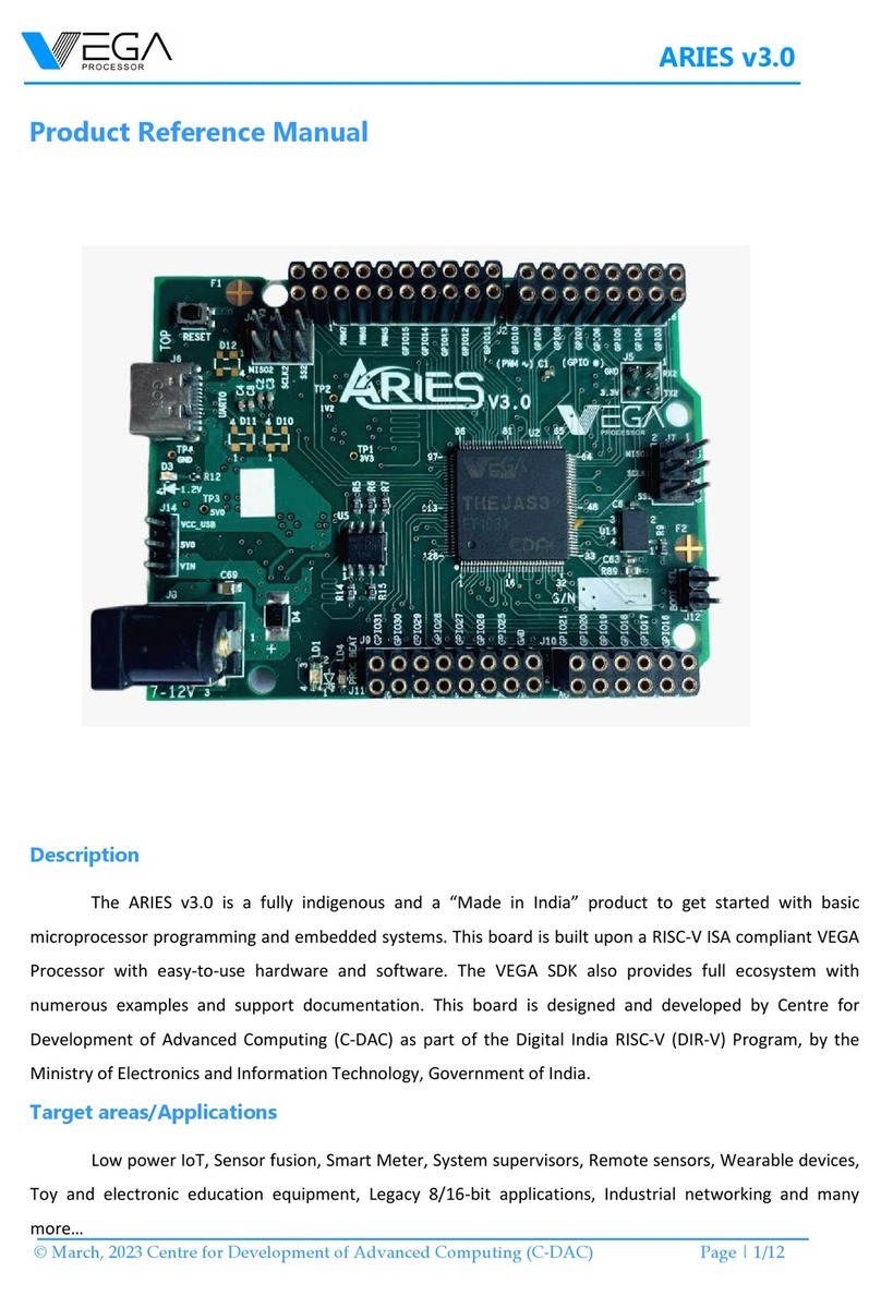
Ref. Description Ref. Description
J8 Po er jack U2 THEJAS32 SoC
J6 USB C Connector U1 3.3V Regulator
RESET Reset Button U4 100 MHz Oscillator
LD1 RGB LED U5 SPI Boot Flash Memory
BTN0 Push Button 0 for GPIO U6 Op-amp
LS1 Buzzer U11 WIFI and Bluetooth Module
3.2 Processor
The main controller is THEAJS32 SoC hich operates at a frequency of 100MHz. It includes VEGA
ET1031 Microprocessor, 256KB internal SRAM, Three UARTs, Four SPIs, Three TIMERs, Eight PWMs, Three
I2C interface, 32 GPIOs. Most of its pins are connected to the external headers, ho ever some are reserved
for internal communication.
3.3 THEJAS32 pinout
Pin # Pin Name Pin Description
Ground reference for IO pins.
IO pins. Connect to 3.3V supply.
SPI 3 Master Out Slave In.
Positive supply for logic. Connect to 1.2V supply.
Ground reference for logic.
Ground reference for IO pins.
Positive supply for IO pins. Connect to 3.3V supply.
Positive supply for logic. Connect to 1.2V supply.
Ground reference for logic.
Connect to GND through a 1K resistor.
JTAG TDO. Left unconnected.
JTAG TMS. Connect to GND through a 1K resistor.
Connect to GND through a 1K resistor.
Ground reference for IO pins.
25 PVDDIO19 Positive supply for IO pins. Connect to 3.3V supply.
Positive supply for logic. Connect to 1.2V supply.
Ground reference for logic.
JTAG TCK. Connect to GND through a 1K resistor


