VMIC VMIVME-3124 User manual

-~
ARTISAN
®
~I
TECHNOLOGY
GROUP
Your definitive source
for
quality
pre-owned
equipment.
Artisan Technology
Group
Full-service,
independent
repair
center
with
experienced
engineers
and
technicians
on staff.
We
buy
your
excess,
underutilized,
and
idle
equipment
along
with
credit
for
buybacks
and
trade-ins
.
Custom
engineering
so
your
equipment
works
exactly as
you
specify.
•
Critical
and
expedited
services
•
Leasing
/
Rentals/
Demos
• In
stock/
Ready-to-ship
•
!TAR-certified
secure
asset
solutions
Expert
team
ITrust
guarantee
I
100%
satisfaction
All
tr
ademarks,
br
a
nd
names, a
nd
br
a
nd
s a
pp
earing here
in
are
th
e property of
th
e
ir
r
es
pecti
ve
ow
ner
s.
Visit our website - Click HERE

VMIVME-3124
ANALOG INPUT BOARD
PRODUCT MANUAL
DOCUMENT NO. 500-003124-000 B
Revised June 10, 1996
VME MICROSYSTEMS INTERNATIONAL CORPORATION
12090 SOUTH MEMORIAL PARKWAY
HUNTSVILLE, ALABAMA 35803-3308
(205) 880-0444
(800) 322-3616
FAX NO. (205) 882-0859

NOTICE
The information in this document has been carefully checked and is believed to be
entirely reliable. While all reasonable efforts to ensure accuracy have been taken in the
preparation of this manual, VMIC assumes no responsibility resulting from omissions or
errors in this manual, or from the use of information contained herein.
VMIC reserves the right to make any changes, without notice, to this or any of
VMIC's products to improve reliability, performance, function, or design.
VMIC does not assume any liability arising out of the application or use of any
product or circuit described herein; nor does VMIC convey any license under its patent
rights or the rights of others.
For warranty and repair polices, refer to VMIC’s Standard Conditions of Sale.
AMXbus, BITMODULE, COSMODULE, DMAbus, IOWorks, IOWorks Access,
IOWorks Foundation, MAGICWARE, MEGAMODULE, PLC ACCELERATOR,
QUICK-R-NET, Soft Logic Link, SRTbus, TESTCAL, “The Next Generation PLC”, The
PLC Connection, TURBOMODULE, UCLIO, UIOD, UPLC, Visual IOWorks, Visual Soft
Logic Control(ler), VMEaccess, VMEmanager, VMEmonitor, VMEnet, VMEnet II,
VMEprobe, and WinUIOC are trademarks of VME Microsystems International
Corporation. The VMIC logo, I/O man figure, and UIOC are registered trademarks of
VME Microsystems International Corporation. Pentuim is a registered trademark of Intel
Corporation. Other registered trademarks are the property of their respective owners.
VME Microsystems International Corporation
All Rights Reserved
This document shall not be duplicated, nor its contents used for any
purpose, unless granted express written permission from VMIC.
Copyright © January 1995 by
VME Microsystems International Corporation

A01/25/95 95-0528
B06/10/96 96-0409
RECORD OF REVISIONS
REVISION
LETTER DATE PAGES INVOLVED CHANGE NUMBER
VME MICROSYSTEMS INT’L CORP.
12090 South Memorial Parkway
Huntsville, AL 35803-3308• (205) 880-0444
REV LTR PAGE NO.
ii
Release
Cover, Pages ii, iii, 3-5, 4-4, 5-4, and
5-6
DOC. NO. 500-003124-000 B

iii
VMIC
SAFETY SUMMARY
THE FOLLOWING GENERAL SAFETY PRECAUTIONS MUST BE OBSERVED DURING ALL PHASES
OF THE OPERATION, SERVICE, AND REPAIR OF THIS PRODUCT. FAILURE TO COMPLY WITH
THESE PRECAUTIONS OR WITH SPECIFIC WARNINGS ELSEWHERE IN THIS MANUAL VIOLATES
SAFETY STANDARDS OF DESIGN, MANUFACTURE, AND INTENDED USE OF THIS PRODUCT.
VME MICROSYSTEMS INTERNATIONAL CORPORATION ASSUMES NO LIABILITY FOR THE
CUSTOMER'S FAILURE TO COMPLY WITH THESE REQUIREMENTS.
GROUND THE SYSTEM
To minimize shock hazard, the chassis and system cabinet must be connected to an
electrical ground. A three-conductor AC power cable should be used. The power cable
must either be plugged into an approved three-contact electrical outlet or used with a
three-contact to two-contact adapter with the grounding wire (green) firmly connected to
an electrical ground (safety ground) at the power outlet.
DO NOT OPERATE IN AN EXPLOSIVE ATMOSPHERE
Do not operate the system in the presence of flammable gases or fumes. Operation of
any electrical system in such an environment constitutes a definite safety hazard.
KEEP AWAY FROM LIVE CIRCUITS
Operating personnel must not remove product covers. Component replacement and
internal adjustments must be made by qualified maintenance personnel. Do not replace
components with power cable connected. Under certain conditions, dangerous voltages
may exist even with the power cable removed. To avoid injuries, always disconnect
power and discharge circuits before touching them.
DO NOT SERVICE OR ADJUST ALONE
Do not attempt internal service or adjustment unless another person, capable of
rendering first aid and resuscitation, is present.
DO NOT SUBSTITUTE PARTS OR MODIFY SYSTEM
Because of the danger of introducing additional hazards, do not install substitute parts or
perform any unauthorized modification to the product. Return the product to VME
Microsystems International Corporation for service and repair to ensure that safety
features are maintained.
DANGEROUS PROCEDURE WARNINGS
Warnings, such as the example below, precede only potentially dangerous procedures
throughout this manual. Instructions contained in the warnings must be followed.
DANGEROUS VOLTAGES, CAPABLE OF CAUSING DEATH, ARE PRESENT IN THIS SYSTEM. USE
EXTREME CAUTION WHEN HANDLING, TESTING, AND ADJUSTING.
WARNING

iv
SAFETY SYMBOLS
OR
***************
***************
*
*
**
*
*
CAUTION
NOTE:
WARNING
!
OR
GENERAL DEFINITIONS OF SAFETY SYMBOLS USED IN
THIS MANUAL
Instruction manual symbol: the product is marked with this symbol when it
is necessary for the user to refer to the instruction manual in order to
protect against damage to the system.
Indicates dangerous voltage (terminals fed from the interior by voltage
exceeding 1000 volts are so marked).
Protective conductor terminal. For protection against electrical shock in
case of a fault. Used with field wiring terminals to indicate the terminal
which must be connected to ground before operating equipment.
Low-noise or noiseless, clean ground (earth) terminal. Used for a signal
common, as well as providing protection against electrical shock in case of
a fault. Before operating the equipment, terminal marked with this symbol
must be connected to ground in the manner described in the installation
(operation) manual.
Frame or chassis terminal. A connection to the frame (chassis) of the
equipment which normally includes all exposed metal structures.
Alternating current (power line).
Direct current (power line).
Alternating or direct current (power line).
The WARNING sign denotes a hazard. It calls attention to a procedure, a
practice, a condition, or the like, which, if not correctly performed or
adhered to, could result in injury or death to personnel.
The CAUTION sign denotes a hazard. It calls attention to an operating
procedure, a practice, a condition, or the like, which, if not correctly
performed or adhered to, could result in damage to or destruction of part or
all of the system.
The NOTE sign denotes important information. It calls attention to a
procedure, a practice, a condition or the like, which is essential to highlight.

500-003124-000
i
SECTION 1. INTRODUCTION
1.1 FEATURES . . . . . . . . . . . . . . . . . . . . . . . . . . . . . . . . . . . . . . . . . . . . . 1-1
SECTION 2. PHYSICAL DESCRIPTION AND SPECIFICATIONS
SECTION 3. THEORY OF OPERATION
3.1 INTRODUCTION . . . . . . . . . . . . . . . . . . . . . . . . . . . . . . . . . . . . . . . . . 3-1
3.2 FUNCTIONAL ORGANIZATION . . . . . . . . . . . . . . . . . . . . . . . . . . . . . 3-1
3.3 VMEbus INTERFACE . . . . . . . . . . . . . . . . . . . . . . . . . . . . . . . . . . . . . 3-1
3.4 ANALOG-TO-DIGITAL CONTROL AND TIMING . . . . . . . . . . . . . . . . 3-3
3.5 BUILT-IN-TEST REFERENCE . . . . . . . . . . . . . . . . . . . . . . . . . . . . . . 3-4
3.6 ANALOG INPUTS . . . . . . . . . . . . . . . . . . . . . . . . . . . . . . . . . . . . . . . . 3-4
3.6.1 Low-Pass Filters . . . . . . . . . . . . . . . . . . . . . . . . . . . . . . . . . . . . . . . . . 3-5
3.6.2 Input Multiplexers. . . . . . . . . . . . . . . . . . . . . . . . . . . . . . . . . . . . . . . . . 3-5
3.6.3 Current Inputs . . . . . . . . . . . . . . . . . . . . . . . . . . . . . . . . . . . . . . . . . . . 3-5
3.7 PROGRAMMABLE GAIN INSTRUMENTATION AMPLIFIER. . . . . . . 3-5
3.8 CHANNEL SEQUENCER AND DUAL-PORTED RAM MEMORY . . . 3-5
3.9 BOARD ID REGISTER . . . . . . . . . . . . . . . . . . . . . . . . . . . . . . . . . . . . 3-6
3.10 BUILT-IN POWER CONVERTER AND ADC POWER SUPPLY. . . . . 3-6
SECTION 4. PROGRAMMING
4.1 MEMORY MAP . . . . . . . . . . . . . . . . . . . . . . . . . . . . . . . . . . . . . . . . . . 4-1
4.2 REGISTER DESCRIPTIONS. . . . . . . . . . . . . . . . . . . . . . . . . . . . . . . . 4-4
4.2.1 Board ID Register . . . . . . . . . . . . . . . . . . . . . . . . . . . . . . . . . . . . . . . . 4-4
4.2.2 Board Configuration Register. . . . . . . . . . . . . . . . . . . . . . . . . . . . . . . . 4-4
4.2.3 Control/Status Register . . . . . . . . . . . . . . . . . . . . . . . . . . . . . . . . . . . . 4-5
4.2.4 Channel Pointer Register. . . . . . . . . . . . . . . . . . . . . . . . . . . . . . . . . . . 4-6
4.2.5 Data Registers . . . . . . . . . . . . . . . . . . . . . . . . . . . . . . . . . . . . . . . . . . . 4-6
4.3 BUILT-IN-TEST FUNCTIONS . . . . . . . . . . . . . . . . . . . . . . . . . . . . . . . 4-8
4.4 RANGE AND GAIN DETERMINATION. . . . . . . . . . . . . . . . . . . . . . . . 4-9
4.5 ACCESSING DATA AS BYTES. . . . . . . . . . . . . . . . . . . . . . . . . . . . . . 4-9
4.6 CURRENT INPUTS, -2BC AND -3BC OPTIONS . . . . . . . . . . . . . . . . 4-10
SECTION 5. CONFIGURATION AND INSTALLATION
5.1 UNPACKING PROCEDURES . . . . . . . . . . . . . . . . . . . . . . . . . . . . . . . 5-1
5.2 PHYSICAL INSTALLATION. . . . . . . . . . . . . . . . . . . . . . . . . . . . . . . . . 5-1
5.3 JUMPER INSTALLATIONS . . . . . . . . . . . . . . . . . . . . . . . . . . . . . . . . . 5-2
VMIVME-3124
ANALOG INPUT BOARD
TABLE OF CONTENTS
Page

500-003124-000
ii
SECTION 5. CONFIGURATION AND INSTALLATION (Concluded) Page
5.3.1 Board Address . . . . . . . . . . . . . . . . . . . . . . . . . . . . . . . . . . . . . . . . . . . 5-2
5.3.2 Address Modifier . . . . . . . . . . . . . . . . . . . . . . . . . . . . . . . . . . . . . . . . . 5-3
5.3.3 Input Configuration. . . . . . . . . . . . . . . . . . . . . . . . . . . . . . . . . . . . . . . . 5-4
5.4 ANALOG INPUT CONNECTOR DESCRIPTION. . . . . . . . . . . . . . . . . 5-5
5.5 CALIBRATION PROCEDURES. . . . . . . . . . . . . . . . . . . . . . . . . . . . . . 5-6
5.5.1 Equipment Required . . . . . . . . . . . . . . . . . . . . . . . . . . . . . . . . . . . . . . 5-6
5.5.2 Instrumentation Amp Offset Calibration . . . . . . . . . . . . . . . . . . . . . . . . 5-6
5.5.3 Unipolar 0-10 V Offset and Gain Calibration . . . . . . . . . . . . . . . . . . . . 5-6
5.5.4 Bipolar ±5 V Offset and Gain Calibration . . . . . . . . . . . . . . . . . . . . . . . 5-7
5.5.5 Bipolar ±10 V Offset and Gain Calibration . . . . . . . . . . . . . . . . . . . . . . 5-7
5.5.6 Built-In-Test Voltage Calibration . . . . . . . . . . . . . . . . . . . . . . . . . . . . . 5-8
SECTION 6. MAINTENANCE
6.1 MAINTENANCE . . . . . . . . . . . . . . . . . . . . 6-1
6.2 MAINTENANCE PRINTS. . . . . . . . . . . . . . . . . 6-1
LIST OF FIGURES
Figure Page
3.2-1 VMIVME-3124 Functional Block Diagram . . . . . . . . . . 3-2
5.3-1 VMIVME-3124 Configuration Jumper Locations . . . . . . . . 5-2
5.4-1 P3 Connector . . . . . . . . . . . . . . . . . . . . . 5-5
LIST OF TABLES
Table Page
4.1-1 VMIVME-3124 Memory Map: Differential Inputs, Normal Buffer . . 4-1
4.1-2 VMIVME-3124 Memory Map: Differential Inputs, Maximum Buffer. . 4-2
4.1-3 VMIVME-3124 Memory Map: Single-Ended Inputs . . . . . . 4-3
4.2.1-1 Board Configuration Register Contents . . . . . . . . . . 4-4
4.2.3-1 Board Control/Status Register Contents . . . . . . . . . . 4-5
4.2.3-2 Board Control/Status Register Modes . . . . . . . . . . 4-6
4.2.5-1 LSB Weight . . . . . . . . . . . . . . . . . . 4-7
4.3-1 BIT Values for 0-10 V Range . . . . . . . . . . . . . 4-8
4.3-2 BIT Values for 5 V Range . . . . . . . . . . . . . . 4-9
4.3-3 BIT Values for 10 V Range . . . . . . . . . . . . . 4-9
4.6-1 Voltage Seen by the ADC . . . . . . . . . . . . . . 4-10
5.3.1-1 Address Selection Jumpers. . . . . . . . . . . . . . 5-3
5.3.2-1 Address Modifier Jumper Settings . . . . . . . . . . . 5-4
5.3.3-1 Input Configuration Jumpers . . . . . . . . . . . . . 5-4
5.4-1 P2 Analog Connector Pinout . . . . . . . . . . . . . 5-5
APPENDIX
Assembly Drawing, Parts List, and Schematic
TABLE OF CONTENTS (Concluded)

500-003124-000
1-1
SECTION 1
INTRODUCTION
1.1 FEATURES
The VMIVME-3124 Analog Input board provides automatic scanning of
16 differential or 32 single-ended analog input channels. The channels are digitized
with a 12-bit resolution Analog-to-Digital Converter (ADC). Each input is over-voltage
protected and low-pass filtered. The board is very easy to use, no software setup is
required. After power-up or system reset, the VMIVME-3124 automatically starts
scanning each of its 16 or 32 input channels. Conversion data is stored automatically
in a dual-port memory, making it immediately accessible from the VMEbus. The
VMIVME-3124 provides on-board voltage references to perform an on-line or off-line
built in self-test. The input voltage range and gain are user programmable with
jumpers. The VMEbus base address and the access mode are fully selectable. In
short I/O space the board can be ordered to support optional current inputs (0-25 mA)
using 32-channel single-ended inputs.
Some of the distinguishing features of the VMIVME-3124 include:
a. VMEbus 3U single height format
b. Sixteen differential or 32 single-ended analog input channels
c. One 12-bit A/D converter with built-in track-and-hold
d. Automatic scanning of all inputs at 40 kHz aggregate rate
e. No software initialization required to begin scanning
f. Input ranges from 50 mV to 10 VDC
g. Input over voltage protection
h. Analog inputs are low pass filtered at 50 kHz
i. Optional add on 40 Hz low pass filter card
j. Discrete wire or mass terminated cables
k. Input pull-down resistors prevent floating inputs
l. Supports on-line & off-line Built-In-Test (BIT)
m. Jumper programmable gains of x1, x10, x100
n. Selectable A/D ranges of 5 VDC, 10 VDC and 0-10 VDC
o. Data Accesses: D16, D08(EO), D08(O)
p. Front panel LED
q. Optional 0-20, 4-20, and 5-25 mA current input range

500-003124-000
1-2
The VMIVME-3124 occupies 128 bytes of short I/O VMEbus addressing
space. Jumpers are provided to place the board on any 128-byte boundary. The board
may also be jumper-programmed to respond to supervisory, nonprivileged, or both
accesses.
Conversion data is available from a 16-bit register (12-bit right justified with
optional sign extension). This data is stored in on-board dual-ported memory for easy
access.
The Built-In-Test (BIT) capability permits the user to verify the on-board ADC
using high precision user programmable reference voltages. Software must control
the BIT functions.
After a system reset, the board returns to a fixed configuration. All bits in the
Control/Status Register are cleared and the front panel FAIL LED is illuminated. The
LED must then be extinguished under software control. This LED can then be used to
visually locate a faulty board in a system.

500-003124-000
2-1
SECTION 2
PHYSICAL DESCRIPTION AND SPECIFICATIONS
REFER TO 800-003124-000 SPECIFICATION

500-003124-000
3-1
SECTION 3
THEORY OF OPERATION
3.1 INTRODUCTION
The VMIVME-3124 is a flexible, low-cost analog input board that provides
16 differential or 32 single-ended analog input channels. The channels are scanned
continuously at an tartrate rate of 40 kHz using a 12-bit resolution Analog-to-Digital
Converter (ADC). Channels are randomly or sequentially read at any time. The current
address of the channel being digitized is read from the Channel Pointer Register.
Scanning is halted at the current channel using the Stop Auto Scan bit in the
Control/Status Register. This disables further channel address increments. The board
then locks onto that channel. This allows a single channel to be digitized every 25sec.
The following sections discuss the functional components of the VMIVME-3124 in detail.
3.2 FUNCTIONAL ORGANIZATION
The VMIVME-3124 is divided into the following functional categories. Each
category will be discussed in detail.
a. VMEbus Interface
b. Analog-to-Digital Converter (ADC) and Control Logic
c. Analog Input Multiplexing, Gain and Conversion
d. BIT Voltage Reference and multiplexer
e. Board ID register
Figure 3.2-1 illustrates the functional blocks of the VMIVME-3124.
3.3 VMEbus INTERFACE
The VMIVME-3124 communications registers are memory mapped as 64 16-bit
words (128-bytes) in memory. The registers are contiguous and can located on any
128-byte boundary within the short I/O space of the VMEbus. The board can be
configured to respond to short supervisory or short nonprivileged data accesses, or both.
See Section 5 for address jumper locations and configurations.

CSR/Status
PGA
ADC Control
ADC Status
16-bit Register
Dual-Port RAM
Gain Select
X1
X10
X100
Sampling 12-bit ADC
Buff
Amp
Ana
Mux
4X2
BIT
Ref
Ana
Mux
32X2
LPF
40Hz
or
50kHz
Mux Select
P3
Analog Inputs
16/32
Differential/
Single-Ended
25MHz
Clock
P1
VMEbus
VMEbus
Foundation
Interface
ADC/CSR/
RAM Control ADC Control
ADC Status
Track
& Hold
12-bit
ADC
Data
Two’s
Complement
500-003124-000
3-2
Figure 3.2-1 VMIVME-3124 Functional Block Diagram
During each read or write operation, all VMEbus control signals are ignored
unless the board selection comparator detects a match between the on-board
selection jumpers and the address and address modifier line from the backplane. The
appropriate board response occurs if a valid match is detected. The open collector
DTACK interface signal is then asserted (driven low). Subsequent completion of the
bus master's read or write cycle causes the board-generated DTACK signal to return
to the OFF state.
After board selection has occurred, three groups of VMEbus signals control
communication with the board. They are as follows:
a. Data bus lines D00 to D15
b. Address lines A01, A02, A03, A04, A05, A06, A07
c. Bus Control Signals:
Write
DS0*, DS1*
SYSCLK
SYSRESET*

500-003124-000
3-3
Data bus lines are bidirectional and move data to and from the board through a
16-bit data transceiver, responding to control signals from the control decoder. The data
transceiver serves as a buffer for the internal data bus that interconnects all data devices
on the board.
Address lines A01 through A07 map the 64 registers into 128-byte range within
the VME address space described in Section 4. The control signals determine whether
data is to be moved to the board (write) or from the board (read). The control signals also
provide the necessary data strobes (DS0,DS1). A SYSRESET input resets all CSR bits.
Static controls are latched into the Control Register and are used primarily to
establish the operational mode of the board.
3.4 ANALOG-TO-DIGITAL CONTROL AND TIMING
Control commands and status flags associated with controlling the
Analog-to-Digital Converter (ADC) are described in Section 4.
There are two modes of operation for this board. The first is to continuously
scan all 16 or 32 analog input channels. The second is to halt scanning and lock onto a
single channel. In either case, the electrical process of analog-to-digital conversion is
similar.
The VMIVME-3124 uses a 12-bit ADC. The ADC has a conversion time of
8.5 sec. Settling time is required for the multiplexers and the Programmable Gain
Amplifier (PGA) before the ADC cycle can begin. The total channel acquisition cycle
occurs every 25 sec. All conversion timing is provided by internal sources. This gives an
aggregate scan rate for all channels of 40 kHz. The ADC’s built-in track/hold amplifier
prevents signals which can vary during a conversion cycle, from giving false ADC
readings.
After the multiplexer and gain amp have settled, the ADC is placed into the
convert mode. The ADC’s BUSY signal then goes active high to indicate the ADC is
currently working on a new conversion cycle. The built-in track/hold amp automatically
changes from track to hold mode, after which the ADC begins its successive
approximation conversion cycle. The conversion digitizes the analog signal from the track
and hold amp into a 12-bit data word.
The ADC signals the completion of its cycle by lowering the BUSY signal to a
logic “0”. If the 2's Complement bit is set in the CSR, the ADC’s 12-bit output is modified
into this format. At this point the 12-bit word is latched for storage to the Dual-Port RAM.

500-003124-000
3-4
3.5 BUILT-IN-TEST REFERENCE
The board is equipped with a programmable precision voltage reference
which is used as a Built-In-Test (BIT) of the board. When selected, the BIT voltage is
transferred through the Programmable Gain Amplifier (PGA) to the Analog-to-Digital
Conversion (ADC), bypassing the external analog input on channel zero. Therefore,
the channel zero location in the Dual-Port RAM is written with the BIT voltage’s
equivalent digital value. After enabling the BIT voltage (Mode 0 bit set), the user
should allow enough time to elapse (810sec max.), to allow sequencing through
channel zero before checking its value. The BIT can be used to test the PGA, the ADC,
and the Dual-Port RAM memory. The BIT may be enabled at any time during initial
board installation or in real time for system self-diagnostics.
The BIT reference is selected from one of three internal precision reference
voltages: +4.980 VDC, +0.4928 VDC, +9.915 mVDC or analog ground (0.0 VDC).
The selection is provided by setting the Mode bits 0,1, and 2 in the
Control/Status Register (CSR) register. See Section 4.
If mode bit 0 is a logical “0”, the board scans all 16 or 32 channels in a
normal mode of operation. If the mode bit is set in the CSR, channel 0 will correspond
to the selected reference voltage VREF0, VREF1, VREF2, or Analog Ground
according to the settings of mode bit 1 and mode bit 2. The digital value received
should be within 10 LSBs of the selected reference voltage. The remaining channels
(1-15 or 1-31) digitize their respective external input sources. Thus, channel zero is
periodically checked during run time to verify the ADC’s operation. Please note that
the current gain and unipolar/bipolar modes must be considered when selecting the
reference voltage. The BIT voltage precedes the PGA and multiplies the reference
voltage selected. Selecting a reference voltage which will exceed the ADC's range
when multiplied by the gain amplifier.
3.6 ANALOG VOLTAGE INPUTS
There are 16 differential or 32 single-ended analog inputs available on the
front panel connector. It is recommended that the differential mode be used for
decreased noise and greater common mode rejection. Unused inputs should be
grounded, including the low side of all unused differential inputs. The board has
internal 22 Mpull-down resistors on the low side of the differential inputs. This
prevents the differential input pair from drifting up past the input multiplexers’
maximum voltage limit.

500-003124-000
3-5
3.6.1 Low Pass Filters
The VMIVME-3124 provides passive single-pole low-pass input filters on all
inputs. The normal -3 dB cut-off frequency is 50 kHz. This provides some high frequency
noise protection for the board. The board may also be configured with an add on daughter
board option. The daughter board provides a low-pass filter with a cut-off frequency of
40 Hz. This lower cut-off provides some protection from local 60 Hz AC line noise. This
option is normally installed by the factory at the time of the order. It can be removed by
the user at a later date if new applications are implemented. If the board is running in
single-ended mode, the user must be sure to install the two zero ohm SIP jumpers in
locations E1 and E2. This allows the low-pass filter to perform in the single-ended
configuration. Adding the 40 Hz daughter board automatically sets the 40 Hz bit in the
CSR register.
3.6.2 Input Multiplexers
The board has two-tiers of analog multiplexing. Each of the 32 inputs is selected
using one of four 8x1 first-tier analog input multiplexers. The second-tier multiplexer is
configured as a 4x2 board. It selects one or two of the first-tier output signals to provide
the single-ended or differential mode of operation. The second-tier multiplexer also
selects the BIT reference voltage if enabled in the Control/Status Register. The
second-tier output is differentially transferred to the Programmable Gain Amplifier (PGA).
3.6.3 Current Inputs
The VMIVME-3124-2BC and -3BC models include current termination resistors
using a daughter board installed in the place of the 40 Hz filter. This allows a current signal
to be terminated to ground. The voltage developed across a resistor is read by the
VMIVME-3124. The optional -2BC board provides resistors value at 250 ±0.01%. The
optional -3BC board provides resistors value at 500 ±0.01%. To support this option the
5 kHz low pass filter is not installed at the factory, all other functionality of the board
remains the same.
NOTE:
THE OPTIONAL -2BC AND -3BC BOARDS ARE CONFIGURED FOR 32-CHANNEL SINGLE-ENDED
MODE ONLY. DIFFERENTIAL INPUTS ARE NOT SUPPORTED.
3.7 PROGRAMMABLE GAIN INSTRUMENTATION AMPLIFIER
Once an input channel has been selected and routed through the input
multiplexers, it enters the PGA as a differential input. The differential amplifier rejects
common mode noise and delivers a scaled, single-ended output to the ADC. The PGA can
be hardware jumpered for gains of 1, 10, and 100. This allows for inputs as low as 50 mV
up to 10 VDC in range. There is no increase in acquisition time for any change in the gain
setting.

500-003124-000
3-6
3.8 CHANNEL SEQUENCER AND DUAL-PORTED RAM MEMORY
The VMIVME-3124 is normally operated in the scanning mode. When the
board is powered up or reset, conversions start immediately. Once the A/D conversion
is completed, the Dual-Port control logic takes the converted data and stores it in the
channel's appropriate Dual-Port register. The channel counter is incremented by one,
which selects the next channel to be multiplexed to the ADC. After selecting the next
channel, a new A/D conversion sequence is initiated. When all input channels have
been converted and stored (16 or 32), the channel counter is reset and the channel
scanning sequence is started again.
The Stop Auto Scan bit in the Control/Status Register may be set to halt the
channel sequencer at its current address. This address may be read from the Channel
Pointer Register. This feature allows the controlling software to lock onto a channel
and digitize it at the maximum rate of 40 kHz. Please note that the desired channel
can not be directly set. The software must wait for the desired channel to appear in the
Channel Pointer register. It then sets the Stop Auto Scan bit within 25 sec.
3.9 BOARD ID REGISTER
The first location in the VMIVME-3124 register set is a read-only Board ID
Register. It always reads $30. Other VMIC products have similar registers which read
different constants. This allows general-purpose system software to automatically
determine any installed boards.
3.10 BUILT-IN POWER CONVERTER AND ADC POWER SUPPLY
Electrical power for the VMIVME-3124 analog circuitry is supplied by an
on-board DC-to-DC converter. The converter transforms +5 VDC power from the
VMEbus into a regulated 15 VDC power. The VMIVME-3124 does not require any
12 VDC from the VMEbus.
The ADC's +5 VDC logic power is provided by an on-board voltage
regulator. Some of the +15 VDC from the DC-to-DC converter’s output is used as the
input voltage to this regulator.

500-003124-000
4-1
SECTION 4
PROGRAMMING
4.1 MEMORY MAP
The VMIVME-3124 occupies 128-bytes of addressing space including four
information and control registers plus the conversion data registers. Tables 4.1-1
through 4.1-3 map this addressing space relative to the base address as set by
configuration jumpers (see Section 5 for details concerning setting the base address and
address modifier jumpers).
The appropriate table is determined by two factors: whether the board is
jumpered for single-ended or differential inputs, and whether the user has selected the
normal or maximum data buffer for differential inputs. If the board is jumpered for
differential inputs and the Max Buffer bit in the Control/Status Register is clear,
Table 4.1-1 applies. If the board is jumpered for differential inputs and the Max Buffer bit
is set, Table 4.1-2 applies. If the board is jumpered for single-ended inputs, Table 4.1-3 is
the only map that applies (see Section 5 for details concerning setting the input
configuration jumpers).
Table 4.1-1. VMIVME-3124 Memory Map: Differential Inputs, Normal Buffer
Offset Address Function Width Access
$00 Board ID Register byte read-only
$01 Configuration Register byte read-only
$02 Control/Status Register byte read/write
$03 Channel Pointer Register byte read-only
$04-$3F Reserved
$40 Channel 0 Data word read/(write)
$42 Channel 1 Data word read/(write)
$44 Channel 2 Data word read/(write)
$46 Channel 3 Data word read/(write)
$48 Channel 4 Data word read/(write)
$4A Channel 5 Data word read/(write)
$4C Channel 6 Data word read/(write)
$4E Channel 7 Data word read/(write)
$50 Channel 8 Data word read/(write)
$52 Channel 9 Data word read/(write)
$54 Channel 10 Data word read/(write)
$56 Channel 11 Data word read/(write)
$58 Channel 12 Data word read/(write)
$5A Channel 13 Data word read/(write)
$5C Channel 14 Data word read/(write)
$5E Channel 15 Data word read/(write)
$60-$7E Reserved

Table 4.1-2. VMIVME-3124 Memory Map: Differential Inputs, Maximum Buffer
Offset
Address Function Width Access
$00 Board ID Register byte read-only
$01 Configuration Register byte read-only
$02 Control/Status Register byte read/write
$03 Channel Pointer Register byte read-only
$04-$3F Reserved
$40 Channel 0 Data word read/(write)
$42 Channel 1 Data word read/(write)
$44 Channel 2 Data word read/(write)
$46 Channel 3 Data word read/(write)
$48 Channel 4 Data word read/(write)
$4A Channel 5 Data word read/(write)
$4C Channel 6 Data word read/(write)
$4E Channel 7 Data word read/(write)
$50 Channel 8 Data word read/(write)
$52 Channel 9 Data word read/(write)
$54 Channel 10 Data word read/(write)
$56 Channel 11 Data word read/(write)
$58 Channel 12 Data word read/(write)
$5A Channel 13 Data word read/(write)
$5C Channel 14 Data word read/(write)
$5E Channel 15 Data word read/(write)
$60 Channel 0 Data word read/(write)
$62 Channel 1 Data word read/(write)
$64 Channel 2 Data word read/(write)
$66 Channel 3 Data word read/(write)
$68 Channel 4 Data word read/(write)
$6A Channel 5 Data word read/(write)
$6C Channel 6 Data word read/(write)
$6E Channel 7 Data word read/(write)
$70 Channel 8 Data word read/(write)
$72 Channel 9 Data word read/(write)
$74 Channel 10 Data word read/(write)
$76 Channel 11 Data word read/(write)
$78 Channel 12 Data word read/(write)
$7A Channel 13 Data word read/(write)
$7C Channel 14 Data word read/(write)
$7E Channel 15 Data word read/(write)
500-003124-000
4-2
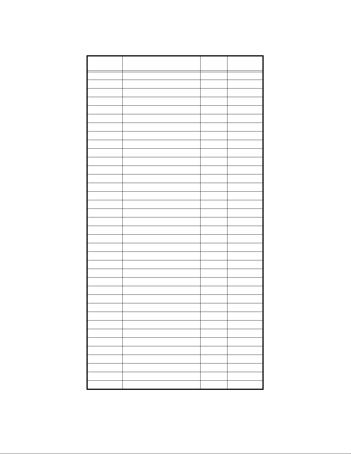
Table 4.1-3. VMIVME-3124 Memory Map: Single-Ended Inputs
Offset
Address Function Width Access
$00 Board ID Register byte read-only
$01 Configuration Register byte read-only
$02 Control/Status Register byte read/write
$03 Channel Pointer Register byte read-only
$04-$3F Reserved
$40 Channel 0 Data word read/(write)
$42 Channel 1 Data word read/(write)
$44 Channel 2 Data word read/(write)
$46 Channel 3 Data word read/(write)
$48 Channel 4 Data word read/(write)
$4A Channel 5 Data word read/(write)
$4C Channel 6 Data word read/(write)
$4E Channel 7 Data word read/(write)
$50 Channel 8 Data word read/(write)
$52 Channel 9 Data word read/(write)
$54 Channel 10 Data word read/(write)
$56 Channel 11 Data word read/(write)
$58 Channel 12 Data word read/(write)
$5A Channel 13 Data word read/(write)
$5C Channel 14 Data word read/(write)
$5E Channel 15 Data word read/(write)
$60 Channel 16 Data word read/(write)
$62 Channel 17 Data word read/(write)
$64 Channel 18 Data word read/(write)
$66 Channel 19 Data word read/(write)
$68 Channel 20 Data word read/(write)
$6A Channel 21 Data word read/(write)
$6C Channel 22 Data word read/(write)
$6E Channel 23 Data word read/(write)
$70 Channel 24 Data word read/(write)
$72 Channel 25 Data word read/(write)
$74 Channel 26 Data word read/(write)
$76 Channel 27 Data word read/(write)
$78 Channel 28 Data word read/(write)
$7A Channel 29 Data word read/(write)
$7C Channel 30 Data word read/(write)
$7E Channel 31 Data word read/(write)
500-003124-000
4-3
Table of contents
Other VMIC Single Board Computer manuals
Popular Single Board Computer manuals by other brands
Motorola
Motorola MVME2600 Series Installation and use manual

Eurotech
Eurotech PROTEUS-1.6-M1G-F2G-GPS user manual
Aaeon
Aaeon GENE-BT05 user manual
SMART Embedded Computing
SMART Embedded Computing MaxCore MC3000 Installation & quick start guide

ADLINK Technology
ADLINK Technology NuPRO-710 Series user guide
TQ-Systems
TQ-Systems TQMLS1028A Preliminary user's manual

