© 2017 www.teamWavelength.com 9
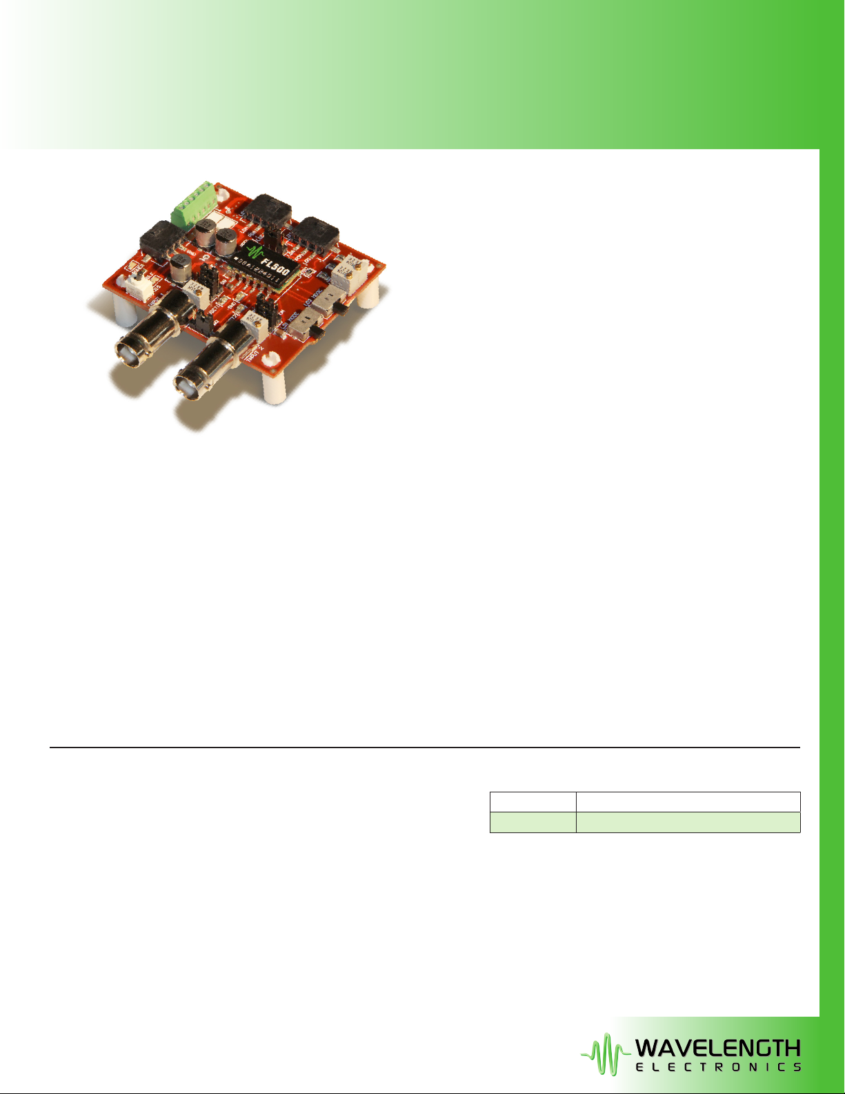
FL591FL LASER DIODE DRIVER
SET THE OUTPUT CONFIGURATION JUMPER
The Output Conguration Jumper (JP2), located between
the output connectors, determines whether the outputs are
paralleled to drive up to 500 mA output on a single channel,
or separate to drive up to 250 mA on two channels.
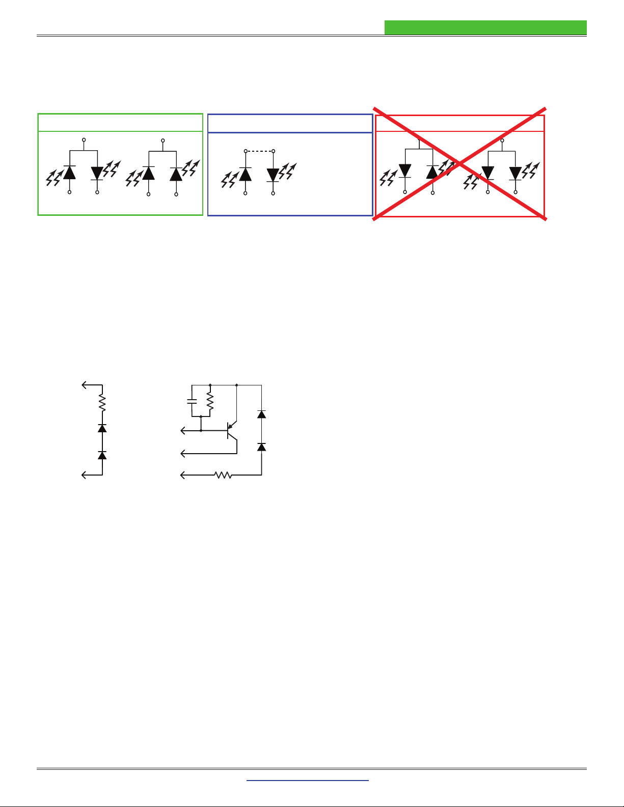
When the driver outputs are separate, connect each laser
diode to the respective output connector, LD1 and LD2.
When the driver outputs are paralleled, each channel
drives one-half of the total output current. When operating
in parallel driver mode, use output connector LD1 to drive
current to the load.
When the FL591FL is delivered, the default conguration
is with two separate 250 mA output channels (jumper set
to “S”).
WIRE THE POWER SUPPLY AND TEST LOAD
Wire the FL591FL power supply according to Figure 2, use
the test load shown in Figure 4.
When the power supply is switched on, power is applied
to the FL500 and the POWER LED will illuminate, but the
output current is not enabled.
SET THE DRIVE CURRENT LIMITS;
SEPARATE OUTPUT CONFIGURATION
First calculate the VLIM voltage; use the transfer function on
page 5 according to your input/output conguration:
VLIM = ILIMx / Transfer Function (Separate) (V)
Connect the DMM to the LIM1 testpoint and the GND
testpoint, and apply power to the FL591FL. Adjust the LIM1
trimpot until the voltage displayed on the DMM matches the
VLIM value calculated above. Turn the trimpot clockwise to
increase the current limit.
Connect the DMM to the LIM2 testpoint, and set the current
limit on channel two using the same procedure.
SET THE DRIVE CURRENT LIMITS;
PARALLEL OUTPUT CONFIGURATION
If the FL591FL is congured to drive paralleled outputs, the
current limit is set using the LIM1 trimpot only.
First calculate the VLIM voltage; use the transfer function on
page 5 based on your input/output conguration:
VLIM = ILIM1 / Transfer Function (Parallel) (V)
Connect the DMM to the LIM1 testpoint and the GND
testpoint, and apply power to the FL591FL. Adjust the LIM1
trimpot until the voltage displayed on the DMM matches the
VLIM value calculated above.
CONFIGURE FOR CONSTANT CURRENT OR
CONSTANT POWER MODE
The FL591FL will drive lasers in Constant Current mode or
Constant Power mode. Constant Power mode operation
requires photodiode feedback from the laser.
To congure channel one for Constant Current mode
operation, set the LD1 MODE switch to CC (left); for
Constant Power mode set the switch to CP (right). Set
channel two in the same manner.
!
donot change swItch posItIons whIle power Is
applIed to the fl591fl. doIng so may damage the
laser. remove power from the fl591fl board
before changIng mode swItch posItIons.
If the FL591FL outputs are paralleled and operated in
CP-mode, the signal on the channel one photodiode is used
in the control feedback loop.
When the FL591FL is delivered, the default conguration is
Constant Current mode on both channels.
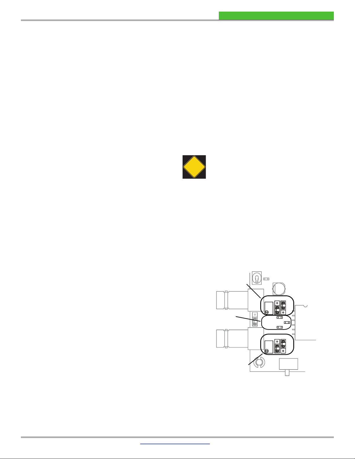
SET THE INPUT SIGNAL CONFIGURATION
Figure 6 shows the setpoint adjust section of the FL591FL.
ENABLE
DIS
INPUT 1
INPUT 2
TRIMPOT
TRIMPOT
BNC
BNC
VSET 1
VSET 2
GND
LD1 MODE
CC
CP
]ON
]OFF
]ONE
]TWO
]OFF
]ON
Channel 2 Controls
SET Testpoints
Channel 1 Controls
LD1 MODE
CC
CP
FL500
Figure 6. Current Setpoint Section
The drivers can be congured to reference only the signal
input on the BNC connector, only the onboard trimpot, or
the sum of the two signals. This versatility allows the driver
to be congured with a bias current set by the trimpot, and
an external modulation signal input on the BNC.