Wavelength Electronics WLD3343 User manual
ORDERING INFORMATION
PART NO DESCRIPTION
WLD3343 2.2 A Laser Diode Driver
WLD3343-3A 3 A Laser Diode Driver
WLD3343HB 2.2 A Li+ Battery-compatible Driver
WLD3343-2L 2.2 A Lower Noise Driver (CC only)
WLD3343-3L 3 A Lower Noise Driver (CC only)
WLD3393 Evaluation PCB
WTW002 Thermal Washer for all WLDs
WHS302 Heatsink for all WLDs
WXC303 +5 VDC Fan for all WLDs
WXC304 +12 VDC Fan for all WLDs
SMALL FOOTPRINT
The WLD3343 is an easy-to-use analog circuit for space
constrained laser diode applications. The WLD3343
maintains precision laser diode current (Constant Current
mode) or stable photodiode current (Constant Power mode)
regulation using electronics that are compatible with any
laser diode type. Safely supply up to 3 A of current (model-
dependent) to a laser diode from a single +5 V power supply.
MODEL VARIATIONS
WLD family. The standard WLD3343 provides up to 2.2 A to
the laser diode. The WLD3343-3A provides up to 3 A. The
WLD3343-2L and WLD3343-3L are lower noise versions
for Constant Current mode of the 2.2 and 3 A models,
respectively. The WLD3343-HB is designed to operate with
lower voltage supplies, including lithium-ion batteries.
RAPID PROTOTYPING
Use the WLD3393 Evaluation Board to rapidly prototype
a complete laser diode control system using the of
the WLD3343 laser diode driver. Onboard switches,
operation simple. Input and output cables are also included
with the WLD3393.
The WLD3343 is excellent for VCSELs, electro-optical
equipment, and medical/dental systems.
ACCESSORIES
In addition to the WLD3393 Evaluation Board, there are
WLD. WEV300 includes a thermal washer and heatsink.
WEV301 adds a +5 V fan, while WEV302 adds a +12 V
fan to the kit. Additionally, there are various power supplies
FEATURES AND BENEFITS
• Low cost
• Slow-start laser diode protection
• Drive up to 3 A output current
• Constant Current or Constant Power operation
• Compatible with any laser diode type
• Small package size (1.3” × 1.26” × 0.3”)
• Voltage-controlled setpoint
• TTL-compatible shutdown pin
• Adjustable current limit
• Adjustable current range
• 2 MHz Constant Current bandwidth
• Over-temperature shutdown
• 14-pin DIP PCB mount
CONTENTS
QUICK CONNECT GUIDE 2
PIN DESCRIPTIONS 4
ELECTRICAL SPECIFICATIONS 6
SAFETY INFORMATION 8
OPERATING INSTRUCTIONS —GENERAL 9
OPERATING INSTRUCTIONS —STANDALONE 10
OPERATING INSTRUCTIONS —WITH EVALUATION BOARD 16
ADDITIONAL TECHNICAL INFORMATION 22
TROUBLESHOOTING 25
MECHANICAL SPECIFICATIONS 26
CERTIFICATION AND WARRANTY 28
e
PAGE
Pb
RoHS
Compliant
© September 2018
A
Laser Type
B
Laser Type
C
Laser Type
406-587-4910
www.teamWavelength.com
WLD3343 & WLD3393
Laser Diode Driver & Evaluation Board
DATASHEET AND OPERATING GUIDE

© 2018 www.teamWavelength.com 2
WLD SERIES LASER DIODE DRIVERS
QUICK CONNECT GUIDE
!
(SOA).
Visit the Wavelength Electronics website for the most
accurate, up-to-date, and easy to use SOA calculator:
www.teamwavelength.com/support/design-tools/soa-ld-calculator/
Enter your operating voltages and currents to determine if
the system will operate robustly or if heatsinking, fan, or
lower voltage power supplies are required.
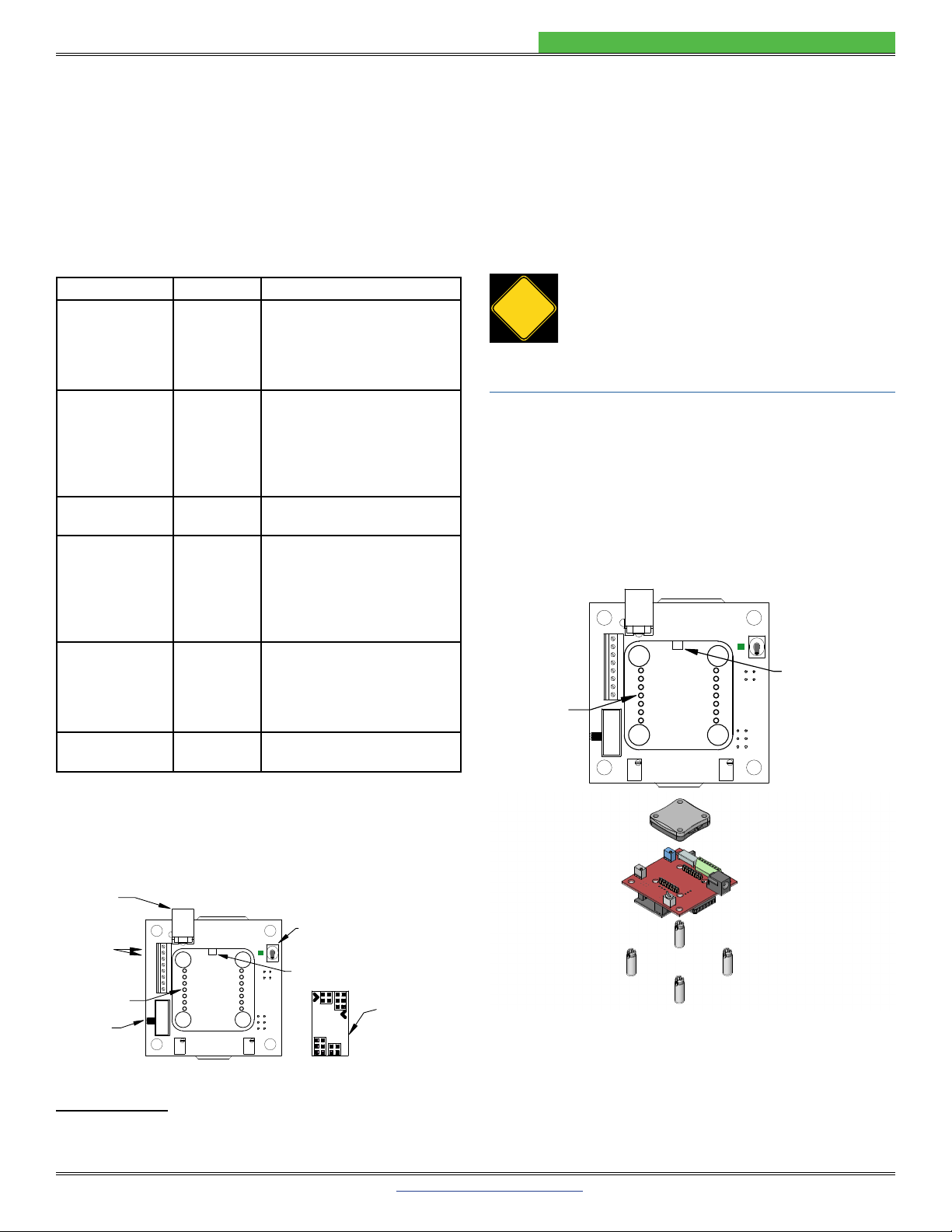
Figure 1 shows the top view of the WLD3343 driver with pin
layout and descriptions.
Figure 2 shows a typical wiring diagram for the WLD3343
driver to operate a Type A or B laser in Constant Current
mode. Refer to page 13 and page 14 for additional
wiring diagrams, including Constant Power wiring diagrams,
and Type C laser wiring diagrams.
An online circuit calculator tool is available, which
automatically determines values for external components,
including RLIM, RSENSE, VSET, along with RPD if operating in
Constant Power mode:
www.teamwavelength.com/support/design-tools/wld-calculator/
1
2
3
4
5
6
7
14
13
12
11
10
9
8
TOP VIEW
SHD
VSET
IMON
PMON
MODE
LIM
GND
VDD
PD-
PD+
OUTA
RS-
OUTB
RS+
Shutdown Laser Diode Output Current
Setpoint Voltage Input
Laser Diode Current Monitor
Photodiode Current Monitor
Mode Configuration
Laser Diode Current Limit
Power Supply Ground
Power Supply Input
Photodiode Current Sense Resistor Negative Input
Photodiode Current Sense Resistor Positive Input
Output A
Laser Diode Current Sense Resistor Negative Input
Output B
Laser Diode Current Sense Resistor Positive Input
Figure 1. Top view and pinout of the WLD3343 laser diode driver.
1
2
3
4
5
6
7
14
13
12
11
10
9
8
WLD3343
LASER
DIODE
DRIVER
VDD
RLIM
1TIE GROUND CONNECTIONS DIRECTLY TO PIN 7
RSENSE
ENABLE
DISABLE
IMON
NC
1kΩ
1
1
1
LD PD LD PD
OR
VDD
D/A
OR OR
Bandgap
Voltage
Reference
VSET
1
1
RPD IPD =VPD
+
-
VPD
RPD
2k
Part # LM4040
www.national.com
1k
LDMAX
SENSE I
00.1
R
With Eval Board (Rev. Level)
Without Evaluation Board
=
V
SET
= (Desired I
LD
) * (2*R
SENSE
)
LD Range RSENSE
(Rev. C)
2.0 A
200 mA
438 mΩ
5.01 Ω
RSENSE
(Rev. A&B)
500 mΩ
5.1 Ω
Figure 2. Quick Connect Diagram: Type A/B laser diodes in Constant Current mode operation.
VALUE DETAILS
VSET Eq. (9) on page 15
IMON Eq. (11) on page 15
RLIM Eq. (7) on page 11
RSENSE Eq. (3) on page 10
Use the online WLD Circuit Calculator to automatically determine
values for external components.
www.teamwavelength.com/support/design-tools/wld-calculator/
© 2018 www.teamWavelength.com 3
WLD SERIES LASER DIODE DRIVERS
RECOMMENDED TEST LOAD
test load with the WLD. The test load takes the place of the
laser diode in the corresponding wiring diagram.
• For standalone operation:
»Type A/B wiring diagrams on page 13.
»Type C wiring diagrams on page 14.
• For operation with the WLD3393 evaluation board:
»Connect the test load across the LDA and LDC
terminals.
When using the test load, the actual drive current can be
determined by measuring the voltage drop across the
resistor. Do not place an ammeter in series with the load
circuit.
Wavelength recommends using a power resistor. The
resistance value is calculated using
RLOAD =VS- 2.5 (1)
ILIM
and the power rating of the resistor is found by
PRLOAD = I2
LIM · RLOAD (2)
For example, if VSis 12 V, and the current limit is 2 A, then
RLOAD
The WLD3343 Series of laser diode drivers are able to drive lasers with any pinout of laser diode and photodiode. Figure 3
Operating Instructions
— General along with the Operating Instructions — Standalone and Operating Instructions — With Evaluation Board
depending on the desired operation.
Type A Laser Diode Type B Laser Diode Type C Laser Diode
Common
Cathode
Laser Diode Anode &
Photodiode Cathode Common Isolated Photodiode
Short the
Laser Diode Anode
to Photodiode Cathode
Common
Anode
Laser Diode Cathode &
Photodiode Anode Common
Figure 3. Laser type diagrams. The WLD3343 can operate Type A, B, and C laser diodes.
© 2018 www.teamWavelength.com 4
WLD SERIES LASER DIODE DRIVERS
PIN DESCRIPTIONS
Table 1. Pin Descriptions
PIN LABEL NAME PIN DESCRIPTION
1 SHD
Shutdown
Laser Diode
Output Current
Enable or disable output current to the laser diode using this pin.
To ENABLE: Float or connect a zero volt signal to this pin.
To DISABLE: Connect a +3 V or greater signal to this pin.
2 VSET
Setpoint
Voltage Input
or Modulation
Input
Connect a voltage source between this pin and Pin 7 (GND) to control either the laser diode
current in Constant Current mode or the laser diode power in Constant Power mode.
Range is 0-2 V full scale.
3 IMON
Laser Diode
Current
Monitor
Monitor the laser diode forward current using this pin. The laser diode current monitor
Standalone: Transfer function depends on RSENSE value. See Equation (11) on page 15.
Evaluation Board: See Table 10 on page 20 for the transfer function.
4 PMON
Photodiode
Current
Monitor
Monitor the laser diode power using this pin. The photodiode current monitor produces a
voltage proportional to the current produced by the laser diode monitor photodiode.
Standalone: Transfer function depends on RPD value. See Equations (12) & (13) on page 15.
Evaluation Board: See Table 11 on page 20 for the transfer function.
5 MODE Mode
Constant Current:
Constant Power:
6 LIM Laser Diode
Current Limit
A resistor connected between this pin and Pin 7 (GND) limits the maximum amount of forward
current through the laser diode. See page 11 for more information.
7 GND Power Supply
Ground Connect the VDD power supply ground connection to this pin.
8 RS+
Laser Diode
Current Sense
Resistor
Positive Input
Connect this pin directly to the positive side of the laser diode current sense resistor. The
resistance value of RSENSE determines the range of forward current through the laser diode.
9 OUTB Output B Connect this pin to the positive side of RSENSE.
10 RS-
Laser Diode
Current Sense
Resistor
Negative Input
Connect this pin directly to the negative side of the laser diode current sense resistor. The
resistance value of RSENSE determines the range of forward current through the laser diode.
11 OUTA Output A
Type A/B: Connect this pin to the cathode connection of the laser diode.
Type C: Connect this pin to Pin 14 (VDD).
12 PD+
Photodiode
Current Sense
Resistor
Positive Input
Constant Current: For all laser types, connect both this pin and Pin 13 (PD-) to Pin 7 (GND).
Constant Power: For Type A/B lasers, connect this pin to the anode of the photodiode. For
Type C lasers, connect this pin to Pin 14 (VDD)
13 PD-
Photodiode
Current Sense
Resistor
Negative Input
Constant Current: For all laser types, connect both this pin and Pin 12 (PD+) to Pin 7 (GND).
Constant Power: For Type A/B lasers, connect this pin to Pin 7 (GND). For Type C lasers,
connect this pin to the cathode of the photodiode.
14 VDD
Power Supply
Input
Power supply input for the internal control electronics.
Supply range input for this pin is model-dependent.

© 2018 www.teamWavelength.com 5
WLD SERIES LASER DIODE DRIVERS
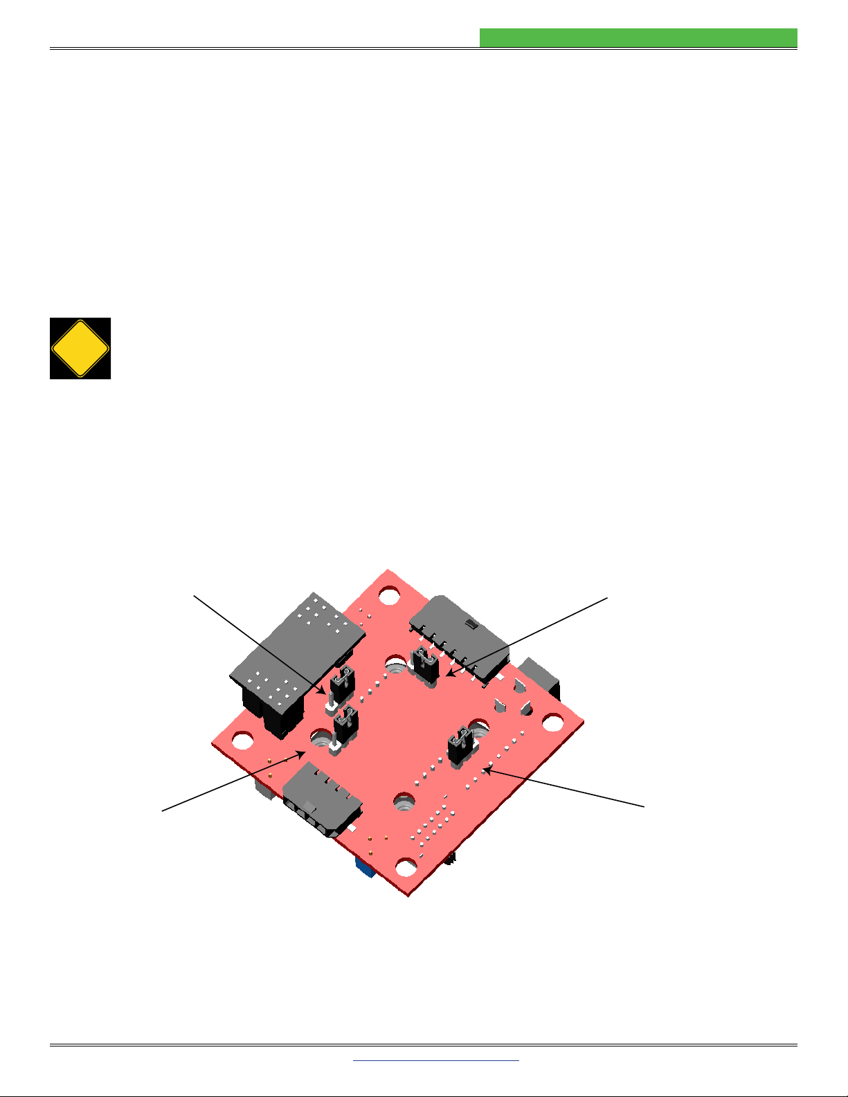
Table 2. Description of jumper connections and functionality on the WLD3393 Evaluation Board.
JUMPER OPTIONS FUNCTION
LD
RANGE 200 mA or 2 A
PD
RANGE
POWER
SELECT
Separate or tied
power supplies
Sand VDD supplies, or to tie the VSand VDD
connections for single supply operation.
VSET
SOURCE T or X
input (X). If a combination of onboard and external setpoints is required, the jumper should be
placed in the “T” position, and an external setpoint connected.
For more information about the jumpers on the bottom of the WLD3393 evaluation board, see page 17.

© 2018 www.teamWavelength.com 6
WLD SERIES LASER DIODE DRIVERS
ELECTRICAL SPECIFICATIONS
PARAMETER SYMBOL VALUE UNIT NOTE
ABSOLUTE MAXIMUM RATINGS
Supply Voltage (at Pin 14) VDD
+4.5 to +12.5
+3.3 to +6 VDC WLD3343, -3A, -2L, -3L
WLD3343HB
Output Current ILD
2.2
3.0 AWLD3343, -2L, HB
WLD3343-3A, -3L
Power Dissipation (TAMBIENT=25°C) PMAX
9
10 WWLD3343, -2L, HB
WLD3343-3A, -3L
Operating Temperature Range
(Case) [1] TOPR
-40 to +85
-40 to +45 ºC WLD3343, -2L, HB
WLD3343-3A, -3L
Storage Temperature Range TSTG -65 to 150 ºC
Weight 0.6 oz 17 grams
Size 1.28 × 1.30 × 0.31 in 32.5 mm x 33.0 mm x 7.9 mm
MODEL
PARAMETER WLD3343HB WLD3343-2A
WLD3343-2L
WLD3343-3A
WLD3343-3L UNIT NOTE
DRIVE CURRENT OUTPUT
Max Output Current 2.2 2.2 3 A
Compliance Voltage,
Laser Diode Load,
VDD = 5 V
3.6 V ILD = 100 mA
3.5 V ILD = 1.0 A
3.0 V ILD = 2.0 A
N/A N/A 2.8 V ILD = 3.0 A
Compliance Voltage,
Laser Diode Load,
VDD = 12 V
N/A 10.6 10.6 V ILD = 100 mA
N/A 10.4 10.4 V ILD = 1.0 A
N/A 10.1 10.1 V ILD = 2.0 A
N/A N/A 9.8 V ILD = 3.0 A
Rise Time 460 ns ILD = Full Scale
Fall Time 320 ns ILD = Full Scale
Bandwidth [2] 2 MHz CC, Sine Wave, 2A
Slow Start – Delay Time 0.24 sec
Slow Start – Ramp Time 0.01 sec
Leakage Current [3] 0 mA
CONSTANT CURRENT CONTROL
Short Term Stability, 1 hour 25 to 50 200 200 ppm TAMBIENT = 25°C
CONSTANT POWER CONTROL
Short Term Stability, 1 hour 0.01 % TAMBIENT = 25°C
Long Term Stability, 24 hours 0.05 % TAMBIENT = 25°C
[1] With Revision D forward of the WLD3343, an internal thermostat has been added to activate Shutdown (SHD) when the internal
temperature exceeds 105°C. The output will be re-enabled after a 250 to 300 ms slow-start once the internal temperature drops below
95°C.
[2] Bandwidth in Constant Power mode depends on photodiode bandwidth.
SENSE. See page 10 for information on setting the current range.
Revision E forward.
Noise: To further reduce noise, the WLD3343-2L and WLD3343-3L models are available. Both are about 2.5 times lower
noise than the WLD3343 and WLD3343-3A, respectively. Constant Power (CP) mode is not available in these models.

© 2018 www.teamWavelength.com 7
WLD SERIES LASER DIODE DRIVERS
ELECTRICAL SPECIFICATIONS (CONTINUED)
MODEL
PARAMETER WLD3343HB WLD3343-2A WLD3343-3A UNIT NOTE
INPUT
MON 1 mV Pin 2, TAMBIENT=25°C, VCM=0 V
VSET Bias Current [4] -50 to 150
VSET Input Voltage Range 0 to 2 V
Power Supply Rejection 80 dB Full Temperature Range
VSET Damage Threshold > VDD + 0.5 or < -0.5 V
VSET Input Impedance 20
THERMAL
Max Internal Power Dissipation
1.2 1.2 2 W TAMBIENT = 25°C
Max Internal Power Dissipation
2 2 3 W TAMBIENT = 25°C
Max Internal Power Dissipation
(Heatsink, Fan) 9 9 10 W TAMBIENT = 25°C
Heatspreader Temperature Rise
TAMBIENT = 25°C
30 °C / W No heatsink, washer, fan.
21.5 °C / W With WHS302 Heatsink,
WTW002 Thermal Washer
3.4 °C / W
With WHS302 Heatsink,
WTW002 Thermal Washer,
and 3.5 CFM Fan
Pin Solderability Time 10 s Solder temperature 260°C
POWER SUPPLY
Voltage, VDD 3.3 to 6 5 to 12 5 to 12 V
Current, VDD Supply, Quiescent 10 mA
MONITOR ACCURACY
Monitor Voltage vs.
Expected Output Current 0.5 % Based on transfer function
PD Monitor vs. Actual 3.3 %
Setpoint vs. Actual 3.5 %
[4] As VSET approaches zero volts, the VSETSET approaches 2 V, the VSET signal source must

© 2018 www.teamWavelength.com 8
WLD SERIES LASER DIODE DRIVERS
SAFETY INFORMATION
SAFE OPERATING AREA — DO NOT EXCEED
INTERNAL POWER DISSIPATION LIMITS
Before attempting to operate the WLD3343 driver, it is
within the Safe Operating Area (SOA). Operating outside
of the SOA may damage the laser and the WLD3343.
Operating outside of the SOA will void the warranty.
To determine if the WLD3343 driver will be operating in a
safe range, follow the instructions for calculating the Safe
Operating Area online with your system’s voltages and
current requirements:
www.teamwavelength.com/support/design-tools/soa-ld-calculator/
SOA charts are included in this datasheet for quick reference
(page 23), but we recommend you use the online tools
instead.
!
If you have any questions about the Safe Operating Area
calculator, call the factory for free and prompt technical
assistance.
THERMAL MANAGEMENT KITS
The WLD Series of laser diode drivers have many thermal
management accessories. They include thermal washers,
heatsinks, and fans. These products are available either as
individual accessories, or bundled together in kits. The use
of these thermal management accessories helps ensure
that the WLD will remain in the SOA during operation.
THEORY OF OPERATION
The WLD Series drivers are voltage controlled current
sources: they deliver the current commanded by the
setpoint. The control system continually monitors the actual
output current, compares it to the setpoint, and adjusts the
It may be useful to remember that you do not directly set
the drive current setpoint; instead, you adjust a voltage
signal that represents the output current. The voltage and
output current are related by a transfer function that varies
by driver model number and maximum current.
The setpoint voltage is adjusted at Pin 2 (VSET). In standalone
operation, this is the only way to vary the setpoint. If using
the evaluation board, there are trimpots that can also adjust
the setpoint.
The adjustable current limit is set by choosing the resistor
RLIM in standalone operation, or with a trimpot if using the
evaluation board.
As current is driven through the laser diode load, there is
a voltage drop across the load because of its impedance.
As the current increases, the voltage drop may increase to
the point that it reaches the Compliance Voltage limit of the
current source. Once that occurs, the current source is no
longer able to increase the current driven to the load even if
you increase the setpoint.
The WLD drivers include features that help protect your
laser and make the driver more versatile in a wide array of
applications:
• The user-adjustable clipping current limit protects the
laser from over-current situations by never allowing
the output current to exceed the user-set limit. If the
setpoint is greater than the limit, the WLD will hold the
output current at the limit.
• Operate in Constant Current or Constant Power mode.
Constant Current keeps the current through the laser
diode constant, while Constant Power keeps the current
through the monitor photodiode constant (proportional
to output power).
• Output current switches on after a 250 ms overall delay
from the time the enable signal is applied.
•
order to have current enabled from the laser driver. To
disable output, connect greater than 3 V to Pin 1.
• Low leakage current, excellent for VCSELs.

© 2018 www.teamWavelength.com 9
WLD SERIES LASER DIODE DRIVERS
OPERATING INSTRUCTIONS
—GENERAL
The WLD3343 drivers have dual in-line pin (DIP) packaging,
and are intended to be mounted onto a circuit board.
Parameters including output current range, output current
limit, photodiode current range, and operating mode are
We recommend using a test load until you are familiar with
operation of the driver. Refer to page 3 for test load
information.
covers generally applicable operating instructions that are
relevant whether or not the optional evaluation board is
operation without the evaluation board (page 10). The
board (page 16).
NECESSARY EQUIPMENT
The following equipment is the minimum necessary to
• WLD3343 controller
• Digital voltmeter, 4-½ digit resolution recommended
•
• Laser diode, mount, and optional temperature control
system
• Recommended heat sink and optional fan
»WTW002 Thermal Washer
»WHS302 Heatsink
»WXC303 (+5 VDC) or WXC304 (+12 VDC) Fan
• Custom circuit board, or WLD3393 evaluation board
• Power supply (see below)
POWER SUPPLY REQUIREMENTS
Linear-regulated or low-noise switching power supplies can
be used. We recommend using power supplies with noise
For WLD3343, WLD3343-3A, WLD3343-2L, WLD3343-3L:
• 4.5 to 12.5 VDC power supply rated for 1.1-times the
maximum laser diode current, plus 150 – 250 mA for
the electronics.
For WLD3343-HB:
• 3.3 to 6 VDC power supply rated for 1.1-times the
maximum laser diode current, plus 150 – 250 mA for
the electronics.
•
Lithium-ion battery or other low voltage power supplies.
PREVENT DAMAGE FROM ELECTROSTATIC
DISCHARGE
Before proceeding, it is critical that you take precautions to
prevent electrostatic discharge (ESD) damage to the driver
and your laser. ESD damage can result from improper
handling of sensitive electronics, and is easily preventable
with simple precautions.
For more information on ESD, see Application Note
AN-LDTC06: Basics: Electrostatic Discharge (ESD).
We recommend that you always observe ESD precautions
when handling the WLD3343 driver and your laser diode.
ONLINE TOOLS AVAILABLE
An online tool, the WLD Circuit Calculator, is available to
assist in the choosing of external components that impact
operation. It is customizable for laser type, and operation
mode. This automatically calculates the required external
component values including RLIM, RSENSE, VSET, and RPD (if
operating in Constant Power mode).
OPERATION MODE
The WLD Series supports Constant Current and Constant
Power modes of operation (with the exception of the -2L
and -3L models, which only support Constant Current).
Depending on the chosen operation mode, either the
current through the laser diode or the current through the
!
Constant current through the laser diode is referred to as
Constant Current mode, and is abbreviated CC. In CC
mode, the setpoint is directly proportional to the laser diode
current.
Constant current through the monitor photodiode is referred
to as Constant Power mode and is abbreviated CP. In CP
mode, the setpoint is directly proportional to the photodiode
current, allowing for control of the power emitted from the
laser diode.

© 2018 www.teamWavelength.com 10
WLD SERIES LASER DIODE DRIVERS
OPERATING INSTRUCTIONS
—STANDALONE
WLD CIRCUIT CALCULATOR
The online WLD Circuit Calculator automatically calculates
the required external component values based on operating
WLD without the calculations found in this section.
SELECT THE LASER DIODE OUTPUT CURRENT
RANGE
The output current range of the WLD3343 depends on the
selection of current sense resistor RSENSE placed between
Pin 8 (RS+) and Pin 10 (RS-) as shown in Figure 4.
TYPE A / B Laser Diodes
A B GND
VDD
11 9 1014
WLD3343
LD
RSENSE
8 7
RS+ RS-
ILD
TYPE C Laser Diodes
A B GND
VDD
11 9 1014
WLD3343
LD
RSENSE
8 7
RS+ RS-
ILD
Figure 4. RSENSE is connected between Pin 8 and Pin 10.
To calculate RSENSE for a maximum desired laser diode current
ILDMAX, use Equation (3) for Constant Power operation and
Equation (4) for Constant Current. Refer to Table 3 to
select RSENSE for common laser diode current ranges.
RSENSE,CP =1.25 (3)
ILDMAX
RSENSE,CC =1.00 (4)
ILDMAX
ILDMAX
CONSTANT
POWER
RSENSE
CONSTANT
CURRENT
RSENSE
50 mA
125 mA
250 mA
500 mA
1.25 A
2.2 A
WLD3343-3A & WLD3343-3L ONLY:
3 A
Table 3. Determine the proper sense resistor (RSENSE)
value based on maximum output current (ILDMAX),
depending on operation mode.
HELPFUL HINTS FOR CHOOSING RSENSE
• SENSE.
• Avoid resistors with high parasitic inductance.
•
• Place RSENSE as close to Pins 8 (RS+) and 10 (RS-) on
the WLD3343 as possible to avoid parasitic resistance
• Use Equation (5) for determining the power rating of
RSENSE.
NOTE: Wavelength Electronics recommends a conservative
power rating of 2 times normal maximum for RSENSE.
Equation (5) incorporates this recommendation.
PRATING = 2 · I2
LDMAX · RSENSE (5)
CHOOSE OPERATION MODE: CC OR CP
The WLD3343 can operate in either Constant Current or
mode is accomplished by installing:
•
Current mode.
•
Power mode.
© 2018 www.teamWavelength.com 11
WLD SERIES LASER DIODE DRIVERS
CONFIGURE THE LASER DIODE CURRENT
LIMIT
The WLD3343 allows a customized current range for
resolution while minimizing output noise. The current limit
is set by properly choosing the limit resistor (RLIM) and
installing it between Pins 6 and 7.
There are two methods of choosing the appropriate
resistance value RLIM normalized
maximum output current and Table 5. The second is a
calculation using Equation (7). Both methods depend on
the laser diode type and mode of operation.
Method 1:
desired laser diode current limit (ILDLIM) by the maximum
laser diode current (ILDMAX), as shown in Equation (6).
Then, choose the resistance value of RLIM shown next to the
calculated normalized maximum output current in Table 5.
IMAX,NORM =ILDLIM (6)
ILDMAX
For example, consider using a Type A/B laser diode in
a maximum current of 2.2 A, and the user wishes to set the
limit current at 1.5 A, then the normalized maximum output
current is 0.68 (1.5/2.2). This value then yields a value of
RLIMTable 5)
Method 2:
To precisely calculate the value of RLIM, use Equation (7),
and Table 4
RLIM =
ILDLIMRSENSE+1
(7)
1- ILDLIMRSENSE+1
LASER DIODE TYPE –MODE
Type A/B – CC 282 2.85
Type A/B – CP 350 3.35
Type C – CC 290 2.93
Type C – CP 385 3.57
Table 4. Values of and to calculate RLIM given laser
type and operation mode.
Setting Current Limits Using Trimpots
Figure 5 to make the maximum current limit adjustable.
GND
7
WLD3343
RLIM
6
LIM
CW CCW
W
150 Ω
500 Ω
SINGLE TURN
TRIMPOT
Figure 5.
limits.
IMAX,NORM
TYPE A/B
CC
RLIM ()
TYPE A/B
CP
RLIM ()
TYPE C
CC
RLIM ()
TYPE C
CP
RLIM ()
0.00 152 149 150 150
0.04 162 160 160 160
0.08 172 171 169 171
0.12 183 183 179 183
0.16 194 195 190 195
0.20 205 208 201 207
0.24 217 222 213 220
0.28 230 236 225 234
0.32 243 251 238 248
0.36 257 267 251 263
0.40 272 284 265 279
0.44 288 301 280 295
0.48 305 320 296 313
0.52 322 340 313 331
0.56 341 361 330 350
0.60 361 383 349 370
0.64 382 406 369 392
0.68 405 432 390 414
0.72 429 459 412 438
0.76 455 488 436 463
0.80 483 519 462 490
0.84 514 552 490 519
0.88 547 588 519 550
0.92 582 627 551 583
0.96 621 670 586 618
1.00 664 716 624 656
Table 5. Choose RLIM as a function of normalized
maximum output current, laser diode type, and operation
mode.
Use the online WLD Circuit Calculator to automatically determine
values for external components.
www.teamwavelength.com/support/design-tools/wld-calculator/

© 2018 www.teamWavelength.com 12
WLD SERIES LASER DIODE DRIVERS
SELECTING THE MONITOR PHOTODIODE
CURRENT RANGE
The monitor photodiode current range determines the
selection of the resistor RPD.
Equation (8) calculates RPD for a maximum desired
photodiode current, IPDMAX. Refer to Table 6 to select RPD for
common photodiode current ranges.
RPD =1(8)
IPDMAX
IPDMAX RPD
2 mA
20 mA
Table 6. Monitor photodiode sense resistor RPD versus
maximum photodiode current IPDMAX
In Constant Power mode, the photodiode is used to control
laser output and RPD is connected across Pin 12 (PD+) and
Pin 13 (PD-). In Constant Current mode, the photodiode is
excluded from the control circuit and Pin 12 (PD+) and Pin
13 (PD-) are shorted together. The photodiode current can
still be monitored in constant current mode with RPD. Refer
to Figure 6 for photodiode resistor connections.
TYPE A / B TYPE C
GND GND
RPD
RPD
VDD
OR
OR
CONSTANT CURRENT
TYPE A / B TYPE C
PD- PD+
GND GND
VDD VDD
PD- PD+
77
13 13
12 12
14 14
OR
PIN 11
WLD3343 WLD3343
OR
PIN 10
RPD RPD
CONSTANT POWER
Figure 6. Connecting RPD
HELPFUL HINTS FOR CHOOSING RPD
• PD.
•
(ppm/°C).
• Place RPD as close to Pins 12 (PD+) and 13 (PD-) on
the WLD3343 as possible to avoid parasitic resistance
mode.
DISABLING OUTPUT CURRENT
The output current can be enabled and disabled as shown
in Figure 7 using a Single-Pole Single-Throw (SPST) switch
or a TTL signal.
!
14 1
VDD WLD3343
ENABLE
DISABLE
SHUTDOWN
SWITCH
SHD
14 1
VDD WLD3343 SHD
TTL INPUT
ENABLE
DISABLE
OR
Figure 7. Enable or disable output current.
Use the online WLD Circuit Calculator to automatically determine
values for external components.
www.teamwavelength.com/support/design-tools/wld-calculator/

© 2018 www.teamWavelength.com 13
WLD SERIES LASER DIODE DRIVERS
CONNECTION DIAGRAMS FOR TYPE A/B LASERS
VALUE DETAILS VALUE DETAILS
VSET Eq. (9) or (10) on page 15 RLIM Eq. (7) on page 11
IMON Eq. (11) on page 15 RSENSE Eq. (3) or (4) on page 10
PMON Eq. (13) on page 15 RPD Eq. (8) on page 12
1
2
3
4
5
6
7
14
13
12
11
10
9
8
WLD3343
LASER
DIODE
DRIVER
VDD
RLIM
1TIE GROUND CONNECTIONS DIRECTLY TO PIN 7
RSENSE
ENABLE
DISABLE
IMON
NC
1kΩ
1
1
1
LD PD LD PD
OR
VDD
D/A
OR OR
Bandgap
Voltage
Reference
VSET
1
1
RPD IPD =VPD
+
-
VPD
RPD
2k
Part # LM4040
www.national.com
1k
LDMAX
SENSE I
00.1
R
With Eval Board (Rev. Level)
Without Evaluation Board
=
V
SET
= (Desired I
LD
) * (2*R
SENSE
)
LD Range RSENSE
(Rev. C)
2.0 A
200 mA
438 mΩ
5.01 Ω
RSENSE
(Rev. A&B)
500 mΩ
5.1 Ω
Figure 8.
1
2
3
4
5
6
7
14
13
12
11
10
9
8
WLD3343
LASER
DIODE
DRIVER
VDD
RPD
RLIM
1TIE GROUND CONNECTIONS DIRECTLY TO PIN 7
RSENSE
ENABLE
DISABLE
IMON
PMON
0.1 µF
1
1
1
LD PD LD PD
OR
VDD
D/A
OR OR
Bandgap
Voltage
Reference
VSET
1
2k
www.national.com
Part #LM4040
1k
PDMAX
PD I
1
R
With Evaluation Board
Without Evaluation Board
=
V
SET
= (Desired I
PD
) * (2*R
PD
)
PD Range RPD
2.0 mA
200 µA
499 Ω
4.99 kΩ
LDMAX
SENSE I
25.1
R
With Eval Board (Rev. Level)
Without Evaluation Board
=
LD Range RSENSE
(Rev. C)
2.0 A
200 mA
438 mΩ
5.01 Ω
RSENSE
(Rev. A&B)
500 mΩ
5.1 Ω
Figure 9.
Use the online WLD Circuit
Calculator to automatically
determine values for external
components.
www.teamwavelength.com/
support/design-tools/wld-
calculator/
Type A Laser Diode
Common
Cathode
Laser Diode Anode &
Photodiode Cathode Common
Type B Laser Diode
Isolated Photodiode
Short the
Laser Diode Anode
to Photodiode Cathode

© 2018 www.teamWavelength.com 14
WLD SERIES LASER DIODE DRIVERS
CONNECTION DIAGRAMS FOR TYPE C LASERS
VALUE DETAILS VALUE DETAILS
VSET Eq. (9) on page 15 RLIM Eq. (7) on page 11
IMON Eq. (11) on page 15 RSENSE Eq. (3) & (4) on page 10
PMON Eq. (13) on page 15 RPD Eq. (8) on page 12
1
2
3
4
5
6
7
14
13
12
11
10
9
8
WLD3343
LASER
DIODE
DRIVER
VDD
RLIM
1TIE GROUND CONNECTIONS DIRECTLY TO PIN 7
RSENSE
ENABLE
DISABLE
IMON
NC
1 kΩ
1
1
1
LD PD LD PD
OR
VDD
D/A
OR OR
Bandgap
Voltage
Reference
VSET
1
RPD IPD =VPD
+
-
VPD
RPD
VDD
2k
Part #LM4040
www.national.com
1k
LDMAX
SENSE I
00.1
R
With Eval Board (Rev. Level)
Without Evaluation Board
=
V
SET
= (Desired I
LD
) * (2*R
SENSE
)
LD Range RSENSE
(Rev. C)
2.0 A
200 mA
438 mΩ
5.01 Ω
RSENSE
(Rev. A&B)
500 mΩ
5.1 Ω
Figure 10.
1
2
3
4
5
6
7
14
13
12
11
10
9
8
WLD3343
LASER
DIODE
DRIVER
RPD
RLIM
1TIE GROUND CONNECTIONS DIRECTLY TO PIN 7
RSENSE
ENABLE
DISABLE
IMON
PMON
0.1µF
1
VDD
D/A
OR OR
Bandgap
Voltage
Reference
VSET
1
VDD
1
LD PD LD PD
OR
2k
Part #LM4040
www.national.com
1k
PDMAX
PD I
1
R
With Evaluation Board
Without Evaluation Board
=
V
SET
= (Desired I
PD
) * (2*R
PD
)
PD Range RPD
2.0 mA
200 µA
499 Ω
4.99 kΩ
LDMAX
SENSE I
25.1
R
With Eval Board (Rev. Level)
Without Evaluation Board
=
LD Range RSENSE
(Rev. C)
2.0 A
200 mA
438 mΩ
5.01 Ω
RSENSE
(Rev. A&B)
500 mΩ
5.1 Ω
Figure 11.
Type C Laser Diode
Common
Anode
Laser Diode Cathode &
Photodiode Anode Common
Use the online WLD Circuit
Calculator to automatically
determine values for external
components.
www.teamwavelength.com/
support/design-tools/wld-
calculator/

© 2018 www.teamWavelength.com 15
WLD SERIES LASER DIODE DRIVERS
UTILIZING VSET (PIN 2)
Pin 2 on the WLD3343, VSET, can be used for externally
Figure 12
!
SET
GND
7
WLD3343
2
VSET
2 kΩ
1 kΩ
DC BIAS
TRIMPOT
2.5 V
Bandgap
Voltage
Reference VPIN2
VDD
OR OR
+
Figure 12.
(left) or a modulated (right) voltage setpoint.
For a given voltage supplied to VSET, either the laser
diode current will change (Constant Current mode), or the
photodiode current will change (Constant Power mode).
Constant Current Mode:
The resulting laser diode current is given by Equation (9).
ILD =VPIN2 (9)
2·RSENSE
Constant Power Mode:
The resulting photodiode current is given by Equation (10).
IPD =VPIN2 (10)
2·RPD
MONITORING THE LASER DIODE CURRENT
(PIN 3)
Pin 3 (IMON) produces a voltage proportional to the current
Equation (11) provides a
transfer function for converting the voltage output of Pin 3 to
the amount of forward current.
ILD =VPIN3 (11)
2·RSENSE
MONITORING THE PHOTODIODE CURRENT
Constant Current and Constant Power mode, due to the
Constant Current Mode:
In Constant Current mode, the photodiode current is
measured directly across RPD. Equation (12) provides
a transfer function for converting this voltage into the
corresponding current through the monitor photodiode.
IPD =VRPD (12)
RPD
Constant Power Mode:
In Constant Power mode, the photodiode current is
measured using Pin 4 (PMON). Equation (13) provides a
transfer function for converting this voltage to the amount of
IPD =VPIN4 (13)
2·RPD
Use the online WLD Circuit Calculator to automatically determine
values for external components.
www.teamwavelength.com/support/design-tools/wld-calculator/
© 2018 www.teamWavelength.com 16
WLD SERIES LASER DIODE DRIVERS
OPERATING INSTRUCTIONS —
WITH EVALUATION BOARD
SETUP INFORMATION
To set up the WLD33931for your project, you’ll need a few
pieces of information. Here’s a handy list of what you’ll need
to know before you start wiring. This is also good information
if you need technical support.
PARAMETER VALUE NOTES
Laser Diode
A, B, or C
See Figure 3 for
schematics. If there is
no photodiode, follow
instructions for Type A laser
diodes.
Power Supply
Voltage
(5-12 V)
If greater than 5 V, make
sure to check the SOA and
use a Thermal Solutions kit
(fan, heatsink, and thermal
washer) or equivalent. HB
model requires less voltage.
Laser Diode
Max Current
Damage threshold for laser
diode.
Operating LD
Current
If greater than 200 mA,
make sure to check the
SOA curve, and use a
Thermal Solutions kit (fan,
heatsink, and thermal
washer) or equivalent.
Operating
Mode CP or CC
CC: Laser diode current is
CP: Laser diode current
varies, photodiode current
Operating PD
Current
Only necessary if output
power will be monitored.
Table 7. WLD setup information
Figure 13 gives a top view of the WLD3393 Evaluation
Board.
Configuration
Board
Laser Diode
A/B TYPE
CC
SET
WLD3343
LASER
DRIVER
P MON
I MON
COM
PGND
VDD
PDC
PDA
LDC
LDA
WAVELENGTH ELECTRONICS
WLD3393
ONLY
0N
(-)
(+)
FAN
PMON
SET
2.5
PDM
CP
COM
LIM
WITH
ENABLE
VS
IMON
OFF
C
USE
1Index Marker
WLD 3343
Sockets
Mode
Switch
Output Current
Enable/Disable
Switch
Fan
Power
Input Cable
Connector
Output Cable Connector
Optional
Supply Input
NOTE:
LINE UP
ARROW WITH
LASER TYPE
INDICATED ON
MAIN BOARD
Figure 13. WLD3393 Top View
1“Additional Technical Information” on page 22 provides
information about using the WLD3393 Evaluation Board with the
WLD3343-HB
CONFIGURING THE EVALUATION BOARD
Follow the next eleven steps sequentially to safely operate
the WLD with your laser diode. Complete steps 1 through 5
before applying power to the board.
WLD3393, it is critical that you verify that the driver will be
within the Safe Operating Area.
!
Wavelength recommends using the online SOA Calculators:
www.teamwavelength.com/support/design-tools/soa-ld-calculator/
Match up the notch in the WLD3343 with the index marker
shown in Figure 14. Align the WLD3343 pins with the
WLD3393 sockets, ensuring that all pins are lined up. Press
Make sure that none of the
pins on the WLD3343 were bent during insertion before
continuing.
A/B TYPE
CC
SET
WLD3343
P MON
I MON
COM
PGND
VDD
PDC
PDA
LDC
LDA
WAVELENGTH ELECTRONICS
WLD3393
ONLY
0N
(-)
(+)
FAN
PMON
SET
2.5
PDM
CP
COM
LIM
WITH
ENABLE
VS
IMON
OFF
C
USE
1Index Marker
WLD 3393
Sockets
Figure 14. Location of index marker and sockets (top)
provided (4-40 ×0.625”).
© 2018 www.teamWavelength.com 17
WLD SERIES LASER DIODE DRIVERS
The two modes of operation supported by the WLD3393 are
Constant Current (CC) and Constant Power (CP):
• In Constant Current mode, VSET correlates directly to
the laser diode current, regardless of laser diode power
intensity.
• In Constant Power mode, the WLD controls the laser
diode using the photodiode to achieve a laser intensity
that is directly proportional to VSET.
Prior to applying power to the board, use the Mode Switch
to choose either CC or CP. Ensure that the switch is
completely rockered to the chosen end.
!
Jumper positions are shown in Figure 15. Factory default
locations are noted.
• LD RANGE Jumper: Select the laser diode output
current range by using the LD RANGE jumper on the
back of the WLD3393. The two available options are
the “200 mA” or the “2 A” position.
• PD RANGE Jumper: Set the PD RANGE jumper on
of your photodiode. It is important to make sure that
the correct PD current range is selected. If the wrong
range is chosen, the WLD3393 may overdrive the laser,
resulting in permanent damage to the laser.
• POWER SELECT Jumper: The factory default is to
separate the VSand VDD power supply inputs. VSdrives
the laser diode while VDD powers the control electronics.
You can tie these together instead by moving the Power
Select jumper to the “VS+VDD” position. Note that when
in this position, VSon the input connector pin will be at
the same potential as the VDD pin.
• VSET SOURCE Jumper: The factory default is to use
the onboard setpoint trimpot to generate the setpoint
voltage (“T” position). To use an external signal, move
this jumper to the “X” position.
VS+VDD
VSET SOURCE
TX
PD RANGE
2 mA
200 µA
LD
RANGE
200 mA
2 Amp
POWER SELECT JUMPER
(separate supplies shown)
LD RANGE JUMPER
(200 mA shown)
PD RANGE JUMPER
(200 μA shown)
VSET SOURCE JUMPER
(use onboard setpoint
trimpot shown)
Figure 15. Jumper locations (factory default), bottom view of WLD3393.

© 2018 www.teamWavelength.com 18
WLD SERIES LASER DIODE DRIVERS
board points to either A/B or C. Refer to Figure 16 for Type
A/B example installation, and Figure 17 for Type C example
installation.
Type A Laser Diode Type B Laser Diode
Common
Cathode
Laser Diode Anode &
Photodiode Cathode Common Isolated Photodiode
Short the
Laser Diode Anode
to Photodiode Cathode
NOTE:
LINE UP
ARROW WITH
LASER TYPE
INDICATED ON
MAIN BOARD
A/B TYPE
CC
SET
WLD3343
P MON
I MON
COM
PGND
VDD
PDC
PDA
LDC
LDA
WAVELENGTH ELECTRONICS
WLD3393
ONLY
0N
(-)
(+)
FAN
PMON
SET
2.5
PDM
CP
COM
LIM
WITH
ENABLE
VS
IMON
OFF
C
USE
1
Set-Up for
Type A/B
Laser Diodes
Figure 16.
Type A/B lasers.
Type C Laser Diode
Common
Anode
Laser Diode Cathode &
Photodiode Anode Common
A/B TYPE
CC
SET
WLD3343
PDC
PDA
LDC
LDA
WAVELENGTH ELECTRONICS
WLD3393
ONLY
0N
(-)
(+)
FAN
PMON
SET
2.5
PDM
CP
COM
LIM
WITH
ENABLE
IMON
OFF
C
USE
1
Set-Up for
Type C
Laser Diodes
P MON
I MON
COM
PGND
VDD
VS
Figure 17.
Type C lasers.
!
This step is optional for less than +5 V, 500 mA operation.
• Heatsink Requirements:
»Attach a heatsink (WHS302) when the WLD3343
will operate between 500 mA and 1.0 A output
current.
»Attach a fan (WXC303 for +5 VDC or WXC304
for +12 VDC) to the heatsink for output currents
exceeding 1.0 A.
»If using Wavelength accessories, refer to the
WHS302, WTW002, WXC303, and/or the
WXC304 datasheets for assembly instructions.
• Fan Connections: Connect the fan leads to the (+)
and (–) fan power positions on the terminal block and
connects to the VDD supply, not VS, so care must be
exercised to ensure that the proper fan is selected,
either +5 VDC or +12 VDC, when using dual power
supplies. Optionally, for lower noise operation, the fan
leads may be connected directly to a separate power
supply compatible with the fan.
DDS
The WLD3393 has two power supply connections:
• VS
»provides power for driving the laser (minimum
current capacity greater than limit current setting).
»can range from +4.5 to +12 V (except for HB
models, must be between +3.3 V and +6 V).
• VDD
»provides power to the control electronics
(minimum 100 mA).
»can range from +5 to +12 V (except for HB
models, must be between +3.3 V and +6 V).
VSand VDD can be connected for simple operation using the
Power Select Jumper. See Step 4 for location.
A separate VSpower supply allows the output current stage
to operate below the minimum 5 V required for the control
electronics or up to the +12 V maxium (for multiple laser
diodes in series). Select VSapproximately 2.0 V above the
maximum voltage drop across the laser diode to reduce the
power dissipation in the WLD3343 component and minimize
your heatsinking requirements. Note that for Type C laser
diodes in Constant Power mode, VDD must be greater than
or equal to VSto keep the photodiode signal in range.
Use PGND for the power return. The common (COM)
terminal on the WLD3393 is not intended to act as a power
connection, but as the low noise ground reference for
connecting an external VSET source, and for monitoring the
IMON, PMON, and PDM signals.
The 2.5 mm input power jack attaches to VDD. You can use
the Wavelength PWRPAK power supplies with this jack. Use
either the power jack or the power inputs on the connector
harness, not both.

© 2018 www.teamWavelength.com 19
WLD SERIES LASER DIODE DRIVERS
The WLD3393 LIM trimpot adjusts the laser diode current
limit from zero to the full 200 mA or 2.2 A, depending on the
laser diode current range selected. For accurate laser diode
A) Connect a test load across the LDA and LDC terminals
of the WLD3393. See page 3 for test load information.
Connect a voltmeter across the test load. This voltmeter
will be used to monitor the output current while setting the
current limit. Refer to the datasheet for your laser diode and
LIMIT),
then calculate the corresponding voltage limit, VLIMIT with
Equation (14).
VLIMIT = ILIMIT · RLOAD (14)
B)
(CC) operation using the Mode Switch.
C) Turn the SET trimpot at least twelve turns counter-
clockwise (OFF). Adjust the LIM trimpot at least twelve turns
clockwise (ON).
D) Apply power to the WLD3393 and enable the output
current by switching the enable switch to the “ON” position.
See Figure 13 to locate the switch.
E) Adjust the SET trimpot clockwise until the voltmeter
displays VLIMIT calculated in Equation (14). Next, turn the
LIM trimpot counter-clockwise until the displayed voltage
just begins to decrease. Finally, turn the SET trimpot fully
counter-clockwise to zero the output current.
F) Disable the output current by switching the enable switch
to the “OFF” position. Remove power from the WLD3393.
G) Return the Mode Switch to CC or CP, according to your
application.
With power removed from the WLD3393 board, connect
the output (4 wire cable) to your laser diode as indicated
in Table 8. Firmly press the output cable into the output
connector.
PIN # WIRE COLOR FUNCTION
1 Red LDA
2 Green PDC
3 White PDA
4 Black LDC
Table 8. Output cable color code.
A Molex 4-pin housing (43645-0400) is the plug used for the
output cable.
© 2018 www.teamWavelength.com 20
WLD SERIES LASER DIODE DRIVERS
IMON, PMON, and PDM allow for monitoring of laser diode
current and power intensity, depending on the selected
mode of operation. All three can be found on the terminal
block. IMON and PMON are duplicated on the input cable
(pinout in Table 9). The voltages at IMON, PMON, and PDM
are all referenced to the common terminal (COM) on the
input connector or the terminal block. A Molex 6-pin housing
(43645-0600) is the plug used for the input cable.
PIN # WIRE COLOR FUNCTION
1 Blue PGND
2 Orange VS
3 Red VDD
4 Black COM
5 White PMON
6 Green IMON
Table 9. Input Cable Color Code
• IMON provides a mechanism for externally monitoring
the laser diode current. IMON is available at all times
in both CC and CP modes. See Table 10 for IMON
transfer functions.
• PMON provides an external indication of the laser diode
intensity by measuring photodiode current. Since PD+
and PD- on the WLD3343 are shorted together in CC
mode, PMON will only monitor photodiode current in
CP mode. See Table 11 for PMON transfer functions
• PDM provides a mechanism for monitoring photodiode
current in either CC or CP mode. While PMON monitors
the feedback used by the control electronics to maintain
constant power of the laser, PDM is an external monitor
that is independent of the control electronics of the
WLD3343. The transfer functions for PDM are the same
as PMON. PDM is accessible on the terminal block.
FUNCTION MODE 200 mA
RANGE
2 A
RANGE
IMON CC / CP 106 mA / V 1.2 A / V
VSET CC 106 mA / V 1.2 A / V
Table 10. WLD3393 laser diode current transfer
functions. Convert IMON and VSET voltage to laser diode
current.
FUNCTION MODE 200 A
RANGE
2 mA
RANGE
PMON CP 1 mA / V
PDM CC / CP 1 mA / V
VSET CP 1 mA / V
Table 11. WLD3393 photodiode current transfer
functions. Convert PMON, PDM, or VSET voltage to
photodiode current.
The setpoint controls the output of the WLD3343. The
setpoint voltage can be adjusted using the onboard
SET trimpot, applying an external setpoint voltage, or by
summing the two signals. The VSET SOURCE jumper
Figure 15 for its location). The sum of the external setpoint
voltage and the SET trimpot voltage can be adjusted
from 0 to 2.5 V. The transfer functions relating the VSET
voltage to the laser diode or photodiode current are given in
Table 10 and Table 11, respectively.
To use only the onboard SET trimpot, place the VSET
SOURCE jumper to the “T” position, and do not connect an
external voltage source to the SET terminal on the terminal
block. The SET trimpot will allow the setpoint to be adjusted
from 0 to 2.5 V.
To use an external voltage source summed with the setpoint
voltage from the onboard SET trimpot, place the VSET
SOURCE jumper to the “T” position. Connect an external
voltage source to the SET terminal on the terminal block.
The resulting setpoint voltage will be the sum of the voltage
dialed in using the SET trimpot, and the voltage applied to
the SET terminal.
To use only an external voltage source for the setpoint,
place the VSET SOURCE jumper to the “X” position and
connect the external setpoint voltage source to the SET
terminal on the terminal block. When the VSET SOURCE
jumper is in the “X” position, the voltage of the SET trimpot
on the WLD3393 is ignored.
If an external voltage source is not available, but setpoint
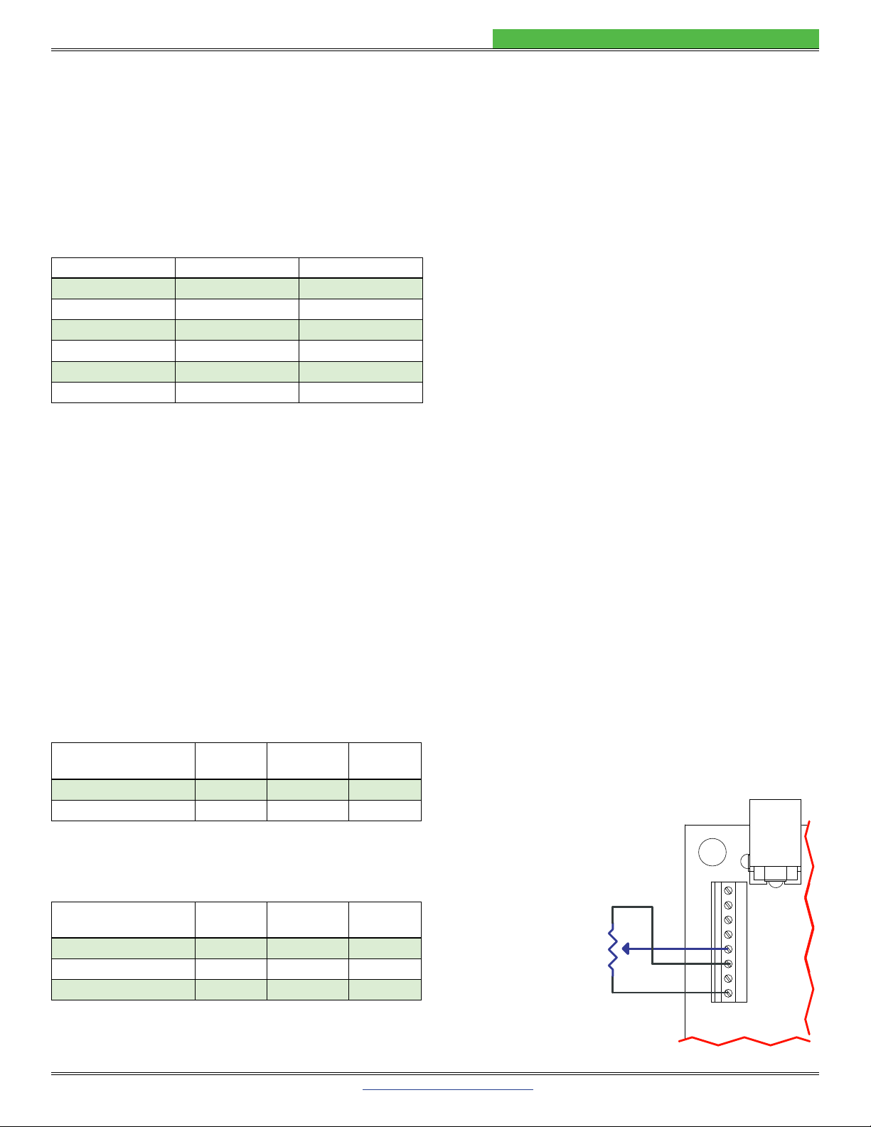
adjustment needs to be external, a remotely located
potentiometer can easily be connected to the WLD3393 to
adjust the setpoint. Connect the clockwise lead of the
potentiometer to the terminal position marked 2.5 on the
terminal block. Connect the counter-clockwise lead to the
COM terminal and connect the wiper to the SET terminal
and ensure that the VSET SOURCE jumper on the bottom
of the board is set to the “X” position. See Figure 18 for
external potentiometer
wiring.
NOTE: The 2.5 V
output can source
1.5 mA with a 5 V input.
resistance to prevent it
loading down.
Figure 18. External
setpoint adjustment.
(-)
(+) FAN
PMON
SET
2.5
PDM
COM
IMON
W
CW
CCW
Other manuals for WLD3343
1
This manual suits for next models
9
Table of contents
Other Wavelength Electronics Motherboard manuals

Wavelength Electronics
Wavelength Electronics WTC32ND User manual

Wavelength Electronics
Wavelength Electronics WLD33ND User manual

Wavelength Electronics
Wavelength Electronics WLD3393 User manual

Wavelength Electronics
Wavelength Electronics WTC3243 User manual

Wavelength Electronics
Wavelength Electronics WTC3293 User manual

Wavelength Electronics
Wavelength Electronics WLD3393 User manual


