winsonic MCH1505S-XN25C User manual

User’s Manua
- Model #M&+1505S-XN25C
WINSONIC ELECTRONICS Co., LTD
No.290-1, Wen Chung Rd., Taoyuan City, Taiwan, R.O.C
l:+886-3-3704789
ax:+886-3-3704722
E-mail:[email protected]
www.ewinsonic.com
Te
F

AD Board Specification
Panel Specification
Safety Instruction
Product Installation
Contents
General Description
Optical Specifications
Absolute Maximum Ratings
Electrical Specifications
Precautions
Assembly
Trouble Shooting
3
4
5
22
5
6
7
18
21
29
30

Safety Instruction
Read and follow these instructions when connecting and using your LCD monitor:
Operation:
1. Keep the monitor out of direct sunlight and away from stoves or any other heat
source.
2. Remove any object that could fall into ventilation holes or prevent proper cooling
of the monitor's electronics.
3. Do not block the ventilation holes on the cabinet.
4. When positioning the monitor, make sure the power plug and outlet are easily
accessible.
5. If turning off the monitor by detaching the power cable or DC power cord, wait
for seconds before attaching the power cable or DC power cord for normal
operation.
6. Do not subject the LCD monitor to severe vibration or high impact conditions
during operation.
7. Do not knock or drop the monitor during operation or transportation.
Maintenance:
8. To protect your display from possible damage, do not put excessive pressure on
the LCD panel. When moving your monitor, grasp the frame to lift; do not lift the
monitor by placing your hand or fingers on the LCD panel.
9. Unplug the monitor if you are not going to use it for an extensive period of time.
10. Unplug the monitor if you need to clean it with a slightly damp cloth. The screen
may be wiped with a dry cloth when the power is off. However, never use organic
solvent, such as, alcohol, or ammonia-based liquids to clean your monitor.
11. To avoid the risk of shock or permanent damage to the set, do not expose the
monitor to dust, rain, water, or excessive moisture environment.
12. If your monitor gets wet, wipe it with dry cloth as soon as possible.
13. If foreign substance or water gets in your monitor, please turn the power off
immediately and disconnect the power cord. Then, remove the foreign substance
or water, and send it to the maintenance center.
14. Do not store or use the LCD monitor in locations exposed to heat, direct sunlight
or extreme cold.
15. In order to maintain the best performance of your monitor and use it for a longer
lifetime, please use the monitor in a location that falls within the following
temperature and humidity ranges. Temperature: 5-35°C 41-95°F

Product Installation
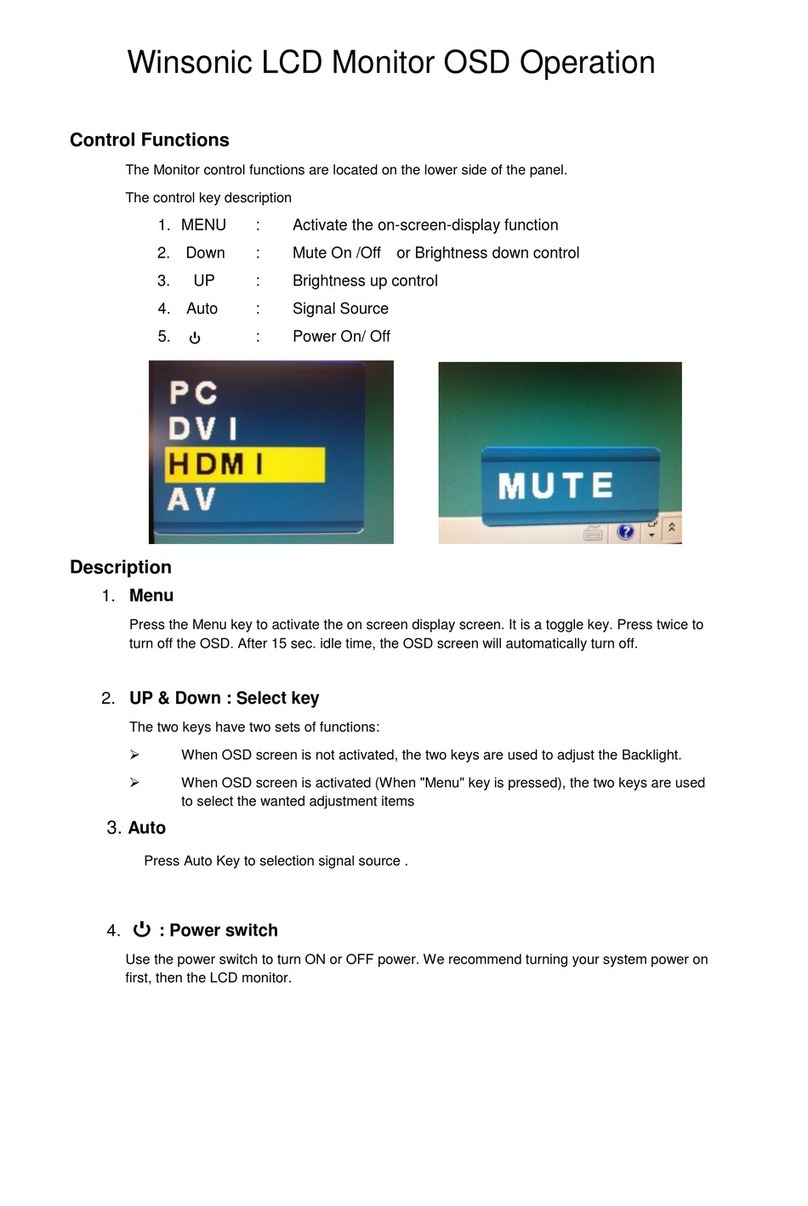
1. Switch off the power on both your monitor and your computer. The Power Switch
is located in the right of the monitor.
2. Connect the power cord to the AC outlet, and connect the power to the monitor
through the AC/DC adapter.
3. VGA Signal-Plug one end of the 15-pin signal cable to the video signal connector
at the rear of the PC system and the other end to the monitor. Secure the
connectors with the screws on the cable connector at both ends.
4. (Optional) DVI Signal-Plug one end of the DVI signal cable to the video signal
connector at the rear of the PC system and the other end to the monitor. Secure
the connectors with the screws on the cable connector at both ends.
5. (Optional) HDMI Signal-Plug one end of the HDMI signal cable to the video
signal connector at the rear of the PC system and the other end to the monitor.
Secure the connectors with the screws on the cable connector at both ends.
6. (Optional) RS232 Connection- Plug one end of RS232 cable to com-port
connector on your PC system and the other end to the monitor. Secure the
connectors with the screws on the cable connector at both ends.

Panel Specification
1. GENERAL DESCRIPTION
1.1 OVERVIEW
MCH1505S-XN25C is a 15.0” TFT Liquid Crystal Display module with 4 CCFL Backlight units and 20 pins LVDS
interface. This module supports 1024 x 768 XGA mode and can display 16.2M. The optimum viewing angle
is at 6 o’clock direction. The inverter module for Backlight is not built in.
1.2 FEATURES
- XGA (1024 x 768 pixels) resolution
- DE (Data Enable) only mode
- LVDS Interface with 1pixel/clock
1.3 APPLICATION
- Desktop monitors
1.4 GENERAL SPECIFICATI0NS etoNtinUnoitacificepSmetI mm)lanogaid”0.51()V(1.822x)H(1.403aerAevitcA mm)V(1.232x)H(2.803aerAgninepOlezeB (1)
--xirtamevitcaTFTiS-atnemelErevirD -lexip867x.B.G.Rx4201rebmuNlexiP -mm)W(792.0x)H(792.0hctiPlexiP --epirtslacitrevBGRtnemegnarrAlexiP -roloc772,491,61sroloCyalpsiD --etihwyllamroNedoMevissimsnarT
1.5 MECHANICAL SPECIFICATIONS
Item Min. Typ. Max. Unit Note
Horizontal(H) - 331.6 - mm
Vertical(V) - 254.76 - mm
Module Size Depth(D) - 13.0 - mm (1)
Weight - - 1,350 g -
Note (1) Please refer to the attached drawings for more information of front and back outline dimensions.

Panel Specification
2. ABSOLUTE MAXIMUM RATINGS
2.1 ABSOLUTE RATINGS OF ENVIRONMENT Value
Item Symbol Min. Max. Unit Note
Storage Temperature TST -20 +60 ºC (1)
Operating Ambient Temperature TOP 0 +50 ºC (1), (2)
HytidimuHegarotS ST 5 85 % -
HytidimuHnoitarepO OP 20 85 % -
Shock (Non-Operating) SNOP - 50 G (3), (5)
Vibration (Non-Operating) VNOP - 2 G (4), (5)
Note (1) Temperature and relative humidity range is shown in the figure below.
(a) 85 %RH Max. (Ta ≦40 ºC).
(b) Wet-bulb temperature should be 39 ºC Max. (Ta > 40 ºC).
(c) No condensation of water.
Note (2) The temperature of panel surface should be 0 ºC Min. and 60 ºC Max.
Note (3) 6ms, 1 time each ±X,±Y and ±Z directions
Note (4) 10 ~ 500 Hz, 1 cycle/20min. 1.5mm max, 1 hour each X, Y and Z directions
Note (5) At testing Vibration and Shock, the fixture in holding the module has to be hard and rigid enough
so that the module would not be twisted or bent by the fixture.
Relative Humidity (%RH)
Operating Range
Temperature (ºC)
100
80600402- 0 20-40
85
80
40
60
20
5Storage Range

Panel Specification
2.2 ELECTRICALABSOLUTE RATINGS
2.2.1 TFT LCD MODULE Value
Item Symbol Min. Max. Unit Note
Power Supply Voltage VDD -0.3 4.0 V
2.2.2 BACKLIGHT UNIT Value
Item Symbol Min. Max. Unit Note
Lamp Voltage VL552 675 VRMS (1), (2), IL= 6.0 mA
Lamp Current IL2.0 6.0 mARMS
Lamp Frequency FL30 80 KHz (1), (2)
Note (1) Permanent damage to the device may occur if maximum values are exceeded. Function operation
should be restricted to the conditions described under Normal Operating Conditions.
Note (2) Specified values are for lamp (Refer to Section 3.2 for further information).

Panel Specification
3. ELECTRICAL CHARACTERISTICS
3.1 TFT LCD MODULE Value
Parameter Symbol Min. Typ. Max. Unit Note
VegatloVylppuSrewoP DD 3.0 3.3 3.6 V -
ItnerruChsuR RUSH - - 1.5 A (2)a)3(Am-053-etihW b)3(Am-035-kcalB
Power Supply Current Vertical Stripe lcc - 450 - mA (3)c
“H” Level VIH - - 100 mV -Differential Input Voltage for
LVDS Receiver Threshold “L” Level VIL -100 - - mV -
RrotsiseRgnitanimreT T- 100 - Ohm -
Note (1) The module should be always operated within above ranges.
Note (2) Measurement Conditions:
470μs
+3.3V
GND
0.9 VDD
0.1 VDD
R1
(High to Low)
(Control Signal)
+12V
SW Q2
C1
1uF
VDD
+3.3V
2SK1470
Q1 2SK1475
47K
R2
1K
VR1 47KC2
0.01uF
C3
1uF
FUSE (LCD Module Input)

Panel Specification
Note (3) The specified power supply current is under the conditions at VDD =3.3V, Ta = 25 ± 2 ºC, DC
Current and fv= 60 Hz, whereas a power dissipation check pattern below is displayed.
3.2 BACKLIGHT UNIT Ta = 25 ± 2 ºC
Value
Parameter Symbol Min. Typ. Max. Unit Note
Lamp Input Voltage VL552 614 675 VRMS IL= 6.0mA
Lamp Current IL2.0 6.0 7.0 mARMS (1)
- - 870 (25 oC) VRMS (2)
Lamp Turn On Voltage VS- - 1090 (0 oC) VRMS (2)
Operating Frequency FL30 45 80 KHz (3)
Lamp Life Time LBL 40,000 50,000 - Hrs (5)
Power Consumption PL- 14740 - mW (4), IL= 6.0 mA
Note (1) Lamp current is measured by utilizing a high frequency current meter as shown below:
Note (2) The voltage shown above should be applied to the lamp for more than 1 second after startup.
Otherwise the lamp may not be turned on.
LCD
Module
1Inverter
A
Current Meter
HV (Pink/ Blue)
LV (White/ Black) 2
Active Area
a. White Pattern
Active Area
b. Black Pattern
Active Area
c. Vertical Stripe Pattern
R
R
R
R
RR
R
R
G
G
G
G
B
B
B
B
B
B
G
G
G
G
B
B
B
B
R
R

Panel Specification
Note (3) The lamp frequency may generate interference with horizontal synchronous frequency from the
display, and this may cause line flow on the display. In order to avoid interference, the lamp
frequency should be detached from the horizontal synchronousfrequency and its harmonics as far
as possible.
Note (4) PL= IL×VL
Note (5) The lifetime of lamp is defined as the time when it continues to operate under the conditions at Ta
= 25 ±2 oC and IL=6.5mARMS until one of the following events occurs:
(a)When the brightness becomes ≦50% of its original value.
(b)When the effective ignition length becomes ≦80% of its original value. (Effective ignition
length is defined as an area that the brightness is less than 70% compared to the center point.)
Note (6) The waveform of the voltage output of inverter must be area-symmetric and the design of the
inverter must have specifications for the modularized lamp. The performance of the Backlight,
such as lifetime or brightness, is greatly influenced by the characteristics of the DC-AC inverter for
the lamp. All the parameters of an inverter should be carefully designed to avoid generating too
much current leakage from high voltage output of the inverter. When designing or ordering the
inverter please make sure that a poor lighting caused by the mismatch of the Backlight and the
inverter (miss-lighting, flicker, etc.) never occurs. If the above situation is confirmed, the module
should be operated in the same manners when it is installed in your instrument.

Panel Specification
4. BLOCK DIAGRAM
4.1 TFT LCD MODULE
4.2 BACKLIGHT UNIT
1 HV
(
Pink
)
2 LV
(
White
)
2
L
V
(
Black
)
2 LV
(
White
)
2 LV
(
Black
)
1 HV
(
Blue
)
1 HV
(
Pink
)
1 HV
(
Blue
)
DC
POWER
SUPPLY
LVDS
INPUT
TFT LCD PANEL
(1024x3x768)
DATA DRIVER IC
SCAN DRIVER IC
BACKLIGHT UNIT
TIMING
CONTROLLER
DC/DC CONVERTER &
REFERENCE VOLTAGE
GENERATOR
INPUT CONNECTOR
(Hirose DF14H-20P-1.25H)
LAMP CONNECTOR
(JST BHSR-02VS-1)
LVDS
INPUT

Panel Specification
5. INPUT TERMINAL PIN ASSIGNMENT
5.1 TFT LCD MODULE
etoNytiraloPnoitcnuFlobmyS.oNniP
1 VDD Power Supply +3.3V(typical)
2 VDD Power Supply +3.3V(typical)
dnuorGDNG3 dnuorGDNG4
5 RX0- LVDS Differential Data Input Negative
6 RX0+ LVDS Differential Data Input Positive
dnuorGDNG7
8 RX1- LVDS Differential Data Input Negative
9 RX1+ LVDS Differential Data Input Positive
dnuorGDNG01
11 RX2- LVDS Differential Data Input Negative
12 RX2+ LVDS Differential Data Input Positive
dnuorGDNG31
14 RXCLK- LVDS Differential Data Input Negative
15 RXCLK+ LVDS Differential Data Input Positive
dnuorGDNG61
17 RX3- LVDS Differential Data Input Negative
18 RX3+ LVDS Differential Data Input Positive
DNGDNG91 devreseRCN02
(1)Connector Part No.: [Hirose] DF14H-20P-1.25H
(2)Matching socket Part No.: [Hirose] DF14-20S-1.25C
5.2 BACKLIGHT UNIT
Pin Symbol Description Color eulB/kniPegatloVhgiH1VH1 kcalB/etihWdnuorGVL2
Note (1) Connector Part No.: BHSR-02VS-1 (JST) or equivalent
Note (2) Matching Connector Part No.: SM02B-BHSS-1-TB (JST) or equivalent

Panel Specification
5.3 COLOR DATA INPUT ASSIGNMENT
The brightness of each primary color (red, green and blue) is based on the 8-bit gray scale data input for
the color. The higher the binary input the brighter the color. The table below provides the assignment of
color versus data input. Data Signal eulBneerGdeR
Color R7 R6 R5 R4 R3 R2 R1 R0 R7 R6 G5 G4 G3 G2 G1 G0 R7 R6 B5 B4 B3 B2 B1 B0
Basic
Colors
Black
Red
Green
Blue
Cyan
Magenta
Yellow
White
0
1
0
0
0
1
1
1
0
1
0
0
0
1
1
1
0
1
0
0
0
1
1
1
0
1
0
0
0
1
1
1
0
1
0
0
0
1
1
1
0
1
0
0
0
1
1
1
0
1
0
0
0
1
1
1
0
1
0
0
0
1
1
1
0
0
1
0
1
0
1
1
0
0
1
0
1
0
1
1
0
0
1
0
1
0
1
1
0
0
1
0
1
0
1
1
0
0
1
0
1
0
1
1
0
0
1
0
1
0
1
1
0
0
1
0
1
0
1
1
0
0
1
0
1
0
1
1
0
0
0
1
1
1
0
1
0
0
0
1
1
1
0
1
0
0
0
1
1
1
0
1
0
0
0
1
1
1
0
1
0
0
0
1
1
1
0
1
0
0
0
1
1
1
0
1
0
0
0
1
1
1
0
1
0
0
0
1
1
1
0
1
Gray
Scale
Of
Red
Red(0) / Dark
Red(1)
Red(2):
:
Red(252)
Red(252)
Red(252)
0
0
0
:
:
1
1
1
0
0
0
:
:
1
1
1
0
0
0
:
:
1
1
1
0
0
0
:
:
1
1
1
0
0
0
:
:
1
1
1
0
0
0
:
:
1
1
1
0
0
1
:
:
0
1
1
0
1
0
:
:
1
0
1
0
0
0
:
:
0
0
0
0
0
0
:
:
0
0
0
0
0
0
:
:
0
0
0
0
0
0
:
:
0
0
0
0
0
0
:
:
0
0
0
0
0
0
:
:
0
0
0
0
0
0
:
:
0
0
0
0
0
0
:
:
0
0
0
0
0
0
:
:
0
0
0
0
0
0
:
:
0
0
0
0
0
0
:
:
0
0
0
0
0
0
:
:
0
0
0
0
0
0
:
:
0
0
0
0
0
0
:
:
0
0
0
0
0
0
:
:
0
0
0
0
0
0
:
:
0
0
0
Gray
Scale
Of
Green
Green(0)/Dark
Green(1)
Green(2)
:
:
Green(252)
Green(252)
Green(252)
0
0
0
:
:
0
0
0
0
0
0
:
:
0
0
0
0
0
0
:
:
0
0
0
0
0
0
:
:
0
0
0
0
0
0
:
:
0
0
0
0
0
0
:
:
0
0
0
0
0
0
:
:
0
0
0
0
0
0
:
:
0
0
0
0
0
0
:
:
1
1
1
0
0
0
:
:
1
1
1
0
0
0
:
:
1
1
1
0
0
0
:
:
1
1
1
0
0
0
:
:
1
1
1
0
0
0
:
:
1
1
1
0
0
1
:
:
0
1
1
0
1
0
:
:
1
0
1
0
0
0
:
:
0
0
0
0
0
0
:
:
0
0
0
0
0
0
:
:
0
0
0
0
0
0
:
:
0
0
0
0
0
0
:
:
0
0
0
0
0
0
:
:
0
0
0
0
0
0
:
:
0
0
0
0
0
0
:
:
0
0
0
Gray
Scale
Of
Blue
Blue(0) / Dark
Blue(1)
Blue(2)
:
:
Blue(252)
Blue(252)
Blue(252)
0
0
0
:
:
0
0
0
0
0
0
:
:
0
0
0
0
0
0
:
:
0
0
0
0
0
0
:
:
0
0
0
0
0
0
:
:
0
0
0
0
0
0
:
:
0
0
0
0
0
0
:
:
0
0
0
0
0
0
:
:
0
0
0
0
0
0
:
:
0
0
0
0
0
0
:
:
0
0
0
0
0
0
:
:
0
0
0
0
0
0
:
:
0
0
0
0
0
0
:
:
0
0
0
0
0
0
:
:
0
0
0
0
0
0
:
:
0
0
0
0
0
0
:
:
0
0
0
0
0
0
:
:
1
1
1
0
0
0
:
:
1
1
1
0
0
0
:
:
1
1
1
0
0
0
:
:
1
1
1
0
0
0
:
:
1
1
1
0
0
0
:
:
1
1
1
0
0
1
:
:
0
1
1
0
1
0
:
:
1
0
1
Note (1) 0: Low Level Voltage, 1: High Level Voltage

Panel Specification
6. INTERFACE TIMING
6.1 INPUT SIGNALTIMING SPECIFICATIONS
The input signal timing specifications are shown as the following table and timing diagram.
Signal Parameter Symbol Min Typ Max Unit Remarks
Pixel clock Frequency Fck - 65 80 MHz
Pixel clock period Tck 12.515 20 ns
Duty ratio (%Tch) - 45 50 55 % Tch/Tck
sn--5hkcTemithgiH
DCLK
sn--5lkcTemitwoL sn--4dsTemitputeS sn--4dhTemitdloH sn--4edsTemitputeS
DATA
DE
sn--4edhTemitdloH
Vertical Frequency Fv - 60 75 Hz
Vertical display active period Tvda 768 768 768 Thp
Vertical display blank period Tvdb 1 38 - Thp
Vertical
Vertical period Tvp 769 806 - Thp
Horizontal display active
period Thda 102410241024 Tck
Horizontal display blank period Thdb 76 320 776 Tck
Horizontal
Horizontal period Thp 110013441800 Tck
Note (1) Because this module is operated by DE only mode, Hsync and Vsync input signals should be set
to low logic level or ground. Otherwise, this module would operate abnormally.

Panel Specification
1
Tvp
Tvda
Tvdb
INPUT SIGNAL TIMING DIAGRAM
Valid display data (1024 Tck)
Tckh
Thde
Tch
Tck
DCLK
DATA
Tsde
ThdTsd
DE Thdb
DCLK
Invalid Valid
DATA
Thp
Thda
0.3VDD
0.5
VDD
2
768 768
DE
0.7VDD
0.3VDD
DE
Tckl
0.7VDD
0.7VDD

Panel Specification
T/7
RESERVED B07 B06 G07 G06 R07 R06
DE GND GND B05 B04 B03 B02
B01 B00 G05 G04 G03 G02 G01
G00 R05 R04 R03 R02 R01 R00
TxCLK OUT
RxCK IN
Rx IN3
Rx IN2
Rx IN1
Rx IN0
TIMING DIAGRAM of LVDS
T
RxOUT23
RxOUT26 RxOUT25 RxOUT24 RxOUT22
RxOUT12 RxOUT9 RxOUT8
RxOUT7 RxOUT6 RxOUT4 RxOUT3 RxOUT2 RxOUT1 RxOUT0
RxOUT21 RxOUT20 RxOUT19
RxOUT18 RxOUT15 RxOUT14 RxOUT13
RxOUT17 RxOUT16 RxOUT11 RxOUT10 RxOUT5 RxOUT27

Panel Specification
6.2 POWER ON/OFF SEQUENCE
Timing Specifications:
0 < t1 ≦10 msec
0 < t2 ≦50 msec
0 < t3 ≦50 msec
t4 ≧1 sec
t5 ≧100 msec
t6 ≧100 msec
Note (1) Please avoid floating state of interface signal at invalid period.
Note (2) When the interface signal is invalid, be sure to pull down the power supply of LCD VDD to 0 V.
Note (3) The Backlight inverter power must be turned on after the power supply for the logic and the
interface signal is valid. The Backlight inverter power must be turned off before the power supply
for the logic and the interface signal is invalid.
-
Power Supply
for LCD, VDD
- Interface Signal
(LVDS Signal of
Transmitter), VI
- Power for Lamp
Restart
Power On Power Off
0V
0V 10%
t6t5
t4
t3t2
t1 10%
90%
10%
90%
Valid Data
ON FFOFFO

Panel Specification
7. OPTICAL CHARACTERISTICS
7.1 TEST CONDITIONS
Item Symbol Value Unit
Ambient Temperature Ta 25±2 oC
aHytidimuHtneibmA 50±10 %RH
Supply Voltage VDD 3.3 V "SCITSIRETCARAHCLACIRTCELE.3"nieulavlacipytotgnidroccAlangiStupnI ItnerruCretrevnI L6.0 mA
The measurement methods of optical characteristics are shown in Section 7.2. The following items
should be measured under the test conditions described in Section 7.1 and stable environment shown in
Note (4).
7.2 OPTICAL SPECIFICATIONS
Item Symbol Condition Min. Typ. Max. UnitNote
052RCoitaRtsartnoC 300 - - (2), (4)
TR- 7 22 ms
Response Time TF- 23 38 ms (3)
m/dc-005054LetihWfoecnanimuLretneC 2(4)
White Uniformity δW 80 85 % (5)
-266.0236.0206.0xR
Red -193.0163.0133.0yR -523.0592.0562.0xG
Green -826.0895.0865.0yG -271.0241.0211.0xB
Blue -231.0201.0270.0yB -443.0413.0482.0xW
Color
Chromaticity
White Wy
θx=0°, θY=0°
Viewing Normal Angle
0.314 0.344 0.374 -
θx+ 50 60 -
Horizontal θx- 50 60 -
θY+ 30 40 -
Viewing Angle Vertical θY-
CR≥10
50 60 -
Deg.
(1), (4)

Panel Specification
Note (1) Definition of Viewing Angle (θx, θy):
Note (2) Definition of Contrast Ratio (CR):
The contrast ratio can be calculated by the following expression.
Contrast Ratio (CR) = L255 / L0
L63: Luminance of gray level 255
L 0: Luminance of gray level 0
CR = CR (5)
CR (X) is corresponding to the Contrast Ratio of the point X at Figure in Note (5).
Note (3) Definition of Response Time (TR, TF):
100%
90%
10%
0%
Gra
y
Level 255
Gray Level 0
Gray Level 255
T
ime
TR
Optical
Response
TF
12 o’clock direction
θy+ = 90º
6 o’clock
θy- = 90º
θx- θx+
θy- θy+
x- y+
y- x+
Normal
θx = θy = 0º
θX+ = 90º
θX- = 90º

Panel Specification
Note (4) Measurement Setup:
The LCD module should be stabilized at given temperature for 20 minutes to avoid abrupt
temperature change during measuring. In order to stabilize the luminance, the measurement
should be executed after lighting Backlight for 20 minutes in a windless room.
Note (5) Definition of White Uniformity (δW):
Measure the luminance of gray level 255 at 5 points
δW = Minimum [L (1), L (2), L (3), L (4), L (5)] / Maximum [L (1), L (2), L (3), L (4), L (5)] * 100%
Photometer
(TOPCON BM-5A)
Field of View = 2º
500 mm
LCD Module
LCD Panel
Center of the Screen
Light Shield Room
(Ambient Luminance < 2 lux)
Active area
Vertical Line Number
Horizontal Line Number
: test point
X=1 to 5
5
1
Horizontal Line Number [pixel]
2
34
0 2565127681023
0
192
384
576
767
X
Table of contents
Other winsonic Monitor manuals

winsonic
winsonic MFC1045S-SN35C User manual

winsonic
winsonic MFM1905S-EN30C User manual

winsonic
winsonic MFC1705S-EN30C User manual

winsonic
winsonic MCH1045S-XN40C User manual

winsonic
winsonic CH1905-EN25L0 User manual

winsonic
winsonic VH-CH6504-QF35L0-0000R-MIL User manual

winsonic
winsonic MFC1045S-XN40C User manual