winsonic VH-CH6504-QF35L0-0000R-MIL User manual

User’s Manual
- Model #VH-CH6504-QF35L0-0000R-MIL
WINSONIC ELECTRONICS Co., LTD
No.290-1, Wen Chung Rd., Taoyuan City, Taiwan, R.O.C
l:+886-3-3704789
ax:+886-3-3704722
E-mail:[email protected]
www.ewinsonic.com
Te
F

Contents
3
4
5
25
5
14
22
Safety Instruction
Product Installation
Panel Specification
General Description
Optical Specifications
Absolute Maximum Ratings
Backlight Unit
Reliability
AD Board Specification
Trouble Shooting
7
28
33

Safety Instruction
Read and follow these instructions when connecting and using your LCD monitor:
Operation:
1. Keep the monitor out of direct sunlight and away from stoves or any other heat
source.
2. Remove any object that could fall into ventilation holes or prevent proper cooling
of the monitor's electronics.
3. Do not block the ventilation holes on the cabinet.
4. When positioning the monitor, make sure the power plug and outlet are easily
accessible.
5. If turning off the monitor by detaching the power cable or DC power cord, wait
for seconds before attaching the power cable or DC power cord for normal
operation.
6. Do not subject the LCD monitor to severe vibration or high impact conditions
during operation.
7. Do not knock or drop the monitor during operation or transportation.
Maintenance:
8. To protect your display from possible damage, do not put excessive pressure on
the LCD panel. When moving your monitor, grasp the frame to lift; do not lift the
monitor by placing your hand or fingers on the LCD panel.
9. Unplug the monitor if you are not going to use it for an extensive period of time.
10. Unplug the monitor if you need to clean it with a slightly damp cloth. The screen
may be wiped with a dry cloth when the power is off. However, never use organic
solvent, such as, alcohol, or ammonia-based liquids to clean your monitor.
11. To avoid the risk of shock or permanent damage to the set, do not expose the
monitor to dust, rain, water, or excessive moisture environment.
12. If your monitor gets wet, wipe it with dry cloth as soon as possible.
13. If foreign substance or water gets in your monitor, please turn the power off
immediately and disconnect the power cord. Then, remove the foreign substance
or water, and send it to the maintenance center.
14. Do not store or use the LCD monitor in locations exposed to heat, direct sunlight
or extreme cold.
15. In order to maintain the best performance of your monitor and use it for a longer
lifetime, please use the monitor in a location that falls within the following
temperature and humidity ranges. Temperature: 5-35°C 41-95°F

Product Installation
1. Switch off the power on both your monitor and your computer. The Power Switch
is located in the right of the monitor.
2. Connect the power cord to the AC outlet, and connect the power to the monitor
through the AC/DC adapter.
3. VGA Signal-Plug one end of the 15-pin signal cable to the video signal connector
at the rear of the PC system and the other end to the monitor. Secure the
connectors with the screws on the cable connector at both ends.
4. (Optional) DVI Signal-Plug one end of the DVI signal cable to the video signal
connector at the rear of the PC system and the other end to the monitor. Secure
the connectors with the screws on the cable connector at both ends.
5. (Optional) HDMI Signal-Plug one end of the HDMI signal cable to the video
signal connector at the rear of the PC system and the other end to the monitor.
Secure the connectors with the screws on the cable connector at both ends.
6. (Optional) RS232 Connection- Plug one end of RS232 cable to com-port
connector on your PC system and the other end to the monitor. Secure the
connectors with the screws on the cable connector at both ends.

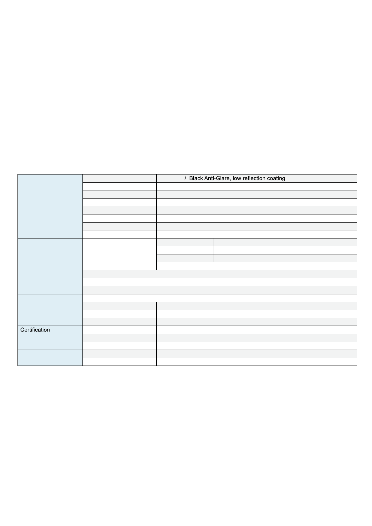
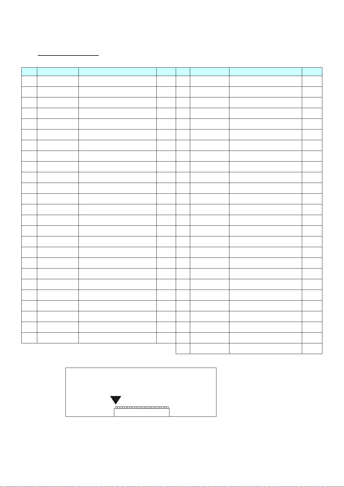
Panel Cell Type / Glass Surface TFT LCD
Aspect Ratio / Size Wide / 65" viewable diagonal area
Active Area / Pixel Pitch 1428.48(H) x 803.52(V) mm / 0.248(H) x 0.744(V) mm
Native Resolution / Colors 3840(H) x 2160(V) / 1.073B
Brightness / Contrast
Response Time
Viewing Angle (typical)
Light Source
Input Sources PC System Signal Analog RGB (0.7/1.0 Vp-p, 75 ohms)
Sync Separate Sync, Composite Sync, Sync On Green
Frequency Fh: 30 - 82Khz , Fv: 50 -75Hz
Audio System 2W speaker x 2
Input Terminals 1 x VGA , 5 x HDMI,1 x DVI,1 x DP , 1 x PC Audio (Stereo Headphone Jack) , 1 x DC Power Plug
Convenient Features Auto Calibration , Back Light Adjustment , Plug&Play (VESA DDC/CI, DDC 2B)
OSD Multi-Languages , Wall Mount Ready (VESA Dimension - please refer to Drawing)
Power Internal power supply with universal / Auto-Sensing, AC90 to 260V, 50/60 Hz
Power Consumption Operation / Power Saving
Operating Condition Temperature / Humidity
Storage Condition Temperature / Humidity
FCC , CE
Dimensions Physical Please refer to Drawing
Carton W x H x D = TBD
Weight N.W. / G.W. 65 Kgs / 69 Kgs
Container Loaded 20ft / 40ft / 40ft HQ TBD (Sets , By pallet)
350 cd/m2(typ) / 5000 : 1
H.176o(- 88o~ + 88o) , V. 176o(- 88o~ + 88o)
LED backlight, Long life, 35,000 hrs (typ)
0oC ~ 50oC (32oF ~ 122oF) , 10% ~ 90% (no condensation)
- 20oC ~ 60oC (- 4oF ~ 140oF) , 10% ~ 90% (no condensation)
2 General Description
This specification applies to the 65 inch Color TFT-LCD Module P650QVF03.0. This LCD module has a
TFT active matrix type liquid crystal panel 3840x2160 pixels. This module supports 3840x2160 mode.
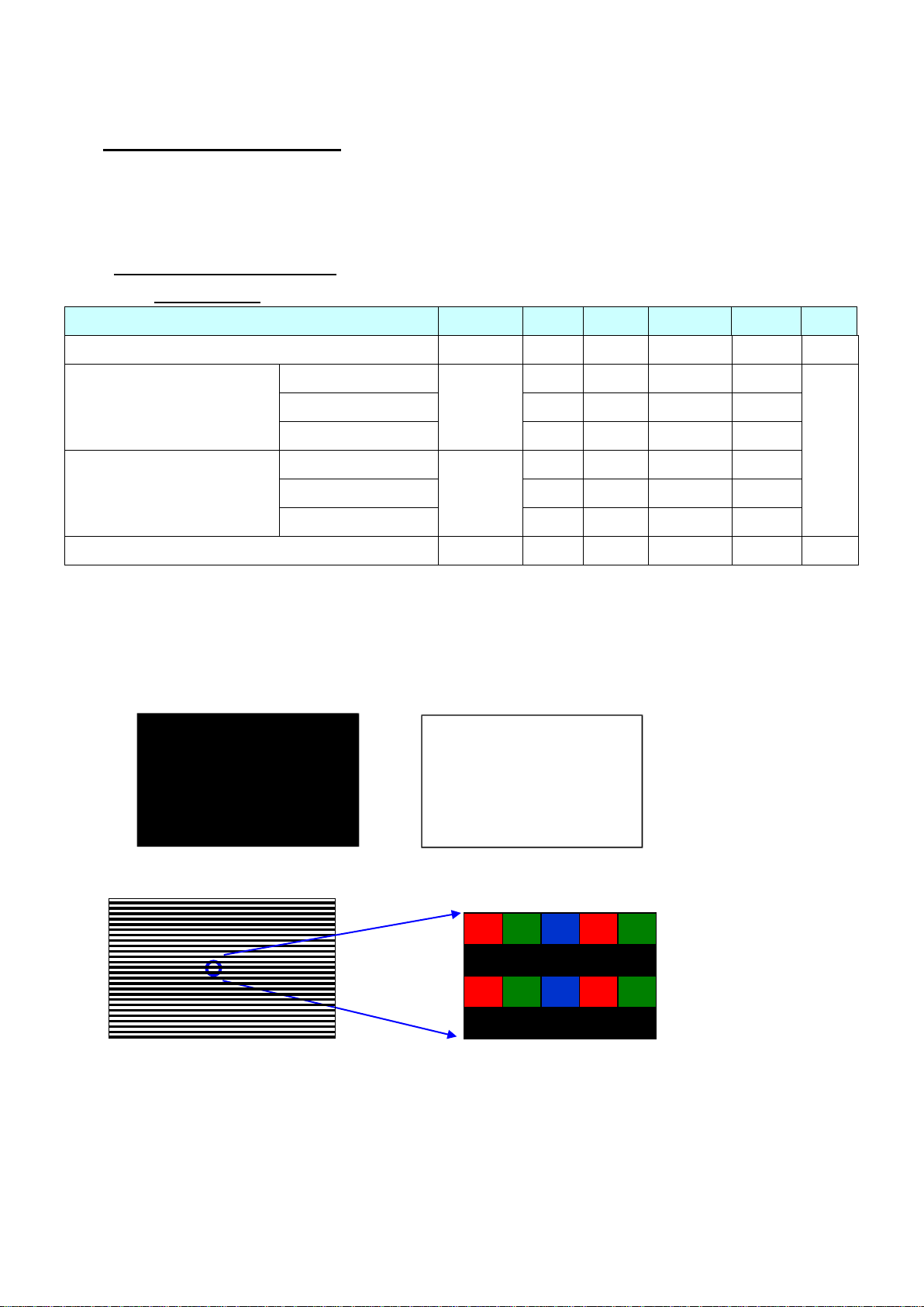
Each pixel is divided into Red, Green and Blue sub-pixels or dots which are arranged in vertical stripes.
Gray scale or the brightness of the sub-pixel color is determined with a 10-bit gray scale signal for each
dot.
260 watt , < 1 watt (Support DPMS)
≤ 6.5 ms (G-to-G)

2. Absolute Maximum Ratings
The followings are maximum values which, if exceeded, may cause faulty operation or damage to the
unit
Item Symbol Min Max Unit Conditions
Logic/LCD Drive Voltage Vcc -0.3 14 [Volt] Note 1
Input Voltage of Signal Vin -0.3 4 [Volt] Note 1
Operating Temperature TOP 0 +50 [oC] Note 2
Operating Humidity HOP 10 90 [%RH] Note 2
Storage Temperature TST -20 +60 [oC] Note 2
Storage Humidity HST 10 90 [%RH] Note 2
Panel Surface Temperature PST --- 65 [oC] Note 3
Note 1: Duration:50 msec.
Note 2 : Maximum Wet-Bulb should be 39℃and No condensation.
The relative humidity must not exceed 90% non-condensing at temperatures of 40℃or less. At
temperatures greater than 40℃, the wet bulb temperature must not exceed 39℃.
Note 3: Surface temperature is measured at 50℃Dry condition

3. Electrical Specification
The P650QVF03.0 requires two power inputs. One is employed to power the LCD electronics and to drive
the TFT array and liquid crystal. The other is to power Back Light Unit.
3.1. Electrical Characteristics
3.1.1 Input Power
Item Symbol Min. Typ. Max Unit Note
Power Supply Input Voltage VDD 10.8 12 13.2 V 1
Power Supply Input Current
Black pattern
IDD
- 1.25 1.5 A
2
White pattern - 3.4 4.08 A
H-strip pattern - 3.28 3.94 A
Power Consumption
Black pattern
PC
- 15 18 Watt
White pattern - 40.8 49.0 Watt
H-strip pattern - 39.4 47.3 Watt
Inrush Current IRUSH -- -- 5 A 3
Note1. The ripple voltage should be fewer than 5% of VDD.
Note2. Test Condition:
(1) VDD = 12.0V, (2) Fv = 60Hz, (3) Fclk= 74.25MHz, (4) Temperature = 25 ℃
(5) Power dissipation check pattern. (Only for power design)
a. Black pattern b. White pattern
c. H-Strip pattern
R G B R G
R G B R G
R G B R G
R G B R G

Note3. Measurement condition : Rising time = 400us
GND
VDD
10%
90%
400
s

3.2 input Connections
LCD connector: (JAE) SJ11346-FI-RTE51SZ-HF
PIN Symbol Description Note PIN Symbol Description Note
1 VDD 12V_PW 26 LCOKN Vx1 LOCK
2 VDD 12V_PW 27 GND Ground
3 VDD 12V_PW 28 RxN0 Vx1 lane 0
4 VDD 12V_PW 29 RxP0 Vx1 lane 0
5 VDD 12V_PW 30 GND Ground
6 VDD 12V_PW 31 RxN1 Vx1 lane 1
7 VDD 12V_PW 32 RxP1 Vx1 lane 1
8 VDD 12V_PW 33 GND Ground
9 NC No connection 2 34 RxN2 Vx1 lane 2
10 GND Ground 35 RxP2 Vx1 lane2
11 GND Ground 36 GND Ground
12 GND Ground 37 RxN3 Vx1 lane 3
13 GND Ground 38 RxP3 Vx1 lane 3
14 GND Ground 39 GND Ground
15 LDC Local Dimming ON/OFF 40 RxN4 Vx1 lane 4
16 NC No connection 2 41 RxP4 Vx1 lane 4
17 NC No connection 2 42 GND Ground
18 NC No connection 2 43 RxN5 Vx1 lane 5
19 NC No connection 2 44 RxP5 Vx1 lane 5
20 NC No connection 2 45 GND Ground
21 GND Ground 46 RxN6 Vx1 lane 6
22 NC No connection 2 47 RxP6 Vx1 lane 6
23 NC No connection 2 48 GND Ground
24 GND Ground 49 RxN7 Vx1 lane 7
25 HTPDN Vx1 HTPDN 50 RxP7 Vx1 lane 7
51 GND Ground
Note1. Pin number start from the left side as the following figure.
PCB
LVDS connector
Pin1 Pin51
Note2. Please leave this pin unoccupied. It can not be connected by any signal (Low/GND/High).

3.3Input Data Format
3.3.1 V by one Data mapping
Mode Packer input & Unpacker
output
30bpp RGB
/YCbCr444
(10bit)
4byte mode
Byte0
D[0] R/Cr[2]
D[1] R/Cr[3]
D[2] R/Cr[4]
D[3] R/Cr[5]
D[4] R/Cr[6]
D[5] R/Cr[7]
D[6] R/Cr[8]
D[7] R/Cr[9]
Byte1
D[8] G/Y[2]
D[9] G/Y[3]
D[10] G/Y[4]
D[11] G/Y[5]
D[12] G/Y[6]
D[13] G/Y[7]
D[14] G/Y[8]
D[15] G/Y[9]
Byte2
D[16] B/Cb[2]
D[17] B/Cb[3]
D[18] B/Cb[4]
D[19] B/Cb[5]
D[20] B/Cb[6]
D[21] B/Cb[7]
D[22] B/Cb[8]
D[23] B/Cb[9]
Byte3
D[24] --
D[25] --
D[26] B/Cb[0]
D[27] B/Cb[1]
D[28] G/Y[0]
D[29] G/Y[1]
D[30] R/Cr[0]
D[31] R/Cr[1]

3.3.2 Color Input Data Reference
The brightness of each primary color (red, green and blue) is based on the 10 bit gray scale data input for the color;
the higher the binary input, the brighter the color. The table below provides a reference for color versus data input.
COLOR DATA REFERENCE
Color
Input Color Data
RED
MSB LSB
GREEN
MSB LSB
BLUE
MSB LSB
R9 R8 R7 R6 R5 R4 R3 R2 R1 R0 G9 G8 G7 G6 G5 G4 G3 G2 G1 G0 B9 B8 B7 B6 B5 B4 B3 B2 B1 B0
Basic
Color
Black 0 0 0 0 0 0 0 0 0 0 0 0 0 0 0 0 0 0 0 0 0 0 0 0 0 0 0 0 0 0
Red(1023) 1 1 1 1 1 1 1 1 1 1 0 0 0 0 0 0 0 0 0 0 0 0 0 0 0 0 0 0 0 0
Green(1023) 0 0 0 0 0 0 0 0 0 0 1 1 1 1 1 1 1 1 1 1 0 0 0 0 0 0 0 0 0 0
Blue(1023) 0 0 0 0 0 0 0 0 0 0 0 0 0 0 0 0 0 0 0 0 1 1 1 1 1 1 1 1 1 1
Cyan 0 0 0 0 0 0 0 0 0 0 1 1 1 1 1 1 1 1 1 1 1 1 1 1 1 1 1 1 1 1
Magenta 1 1 1 1 1 1 1 1 1 1 0 0 0 0 0 0 0 0 0 0 1 1 1 1 1 1 1 1 1 1
Yellow 1 1 1 1 1 1 1 1 1 1 1 1 1 1 1 1 1 1 1 1 0 0 0 0 0 0 0 0 0 0
White 1 1 1 1 1 1 1 1 1 1 1 1 1 1 1 1 1 1 1 1 1 1 1 1 1 1 1 1 1 1
R
RED(000) 0 0 0 0 0 0 0 0 0 0 0 0 0 0 0 0 0 0 0 0 0 0 0 0 0 0 0 0 0 0
RED(001) 0 0 0 0 0 0 0 0 0 1 0 0 0 0 0 0 0 0 0 0 0 0 0 0 0 0 0 0 0 0
----
RED(1022) 1 1 1 1 1 1 1 1 1 0 0 0 0 0 0 0 0 0 0 0 0 0 0 0 0 0 0 0 0 0
RED(1023) 1 1 1 1 1 1 1 1 1 1 0 0 0 0 0 0 0 0 0 0 0 0 0 0 0 0 0 0 0 0
G
GREEN(000) 0 0 0 0 0 0 0 0 0 0 0 0 0 0 0 0 0 0 0 0 0 0 0 0 0 0 0 0 0 0
GREEN(001) 0 0 0 0 0 0 0 0 0 0 0 0 0 0 0 0 0 0 0 1 0 0 0 0 0 0 0 0 0 0
----
GREEN(1022) 0 0 0 0 0 0 0 0 0 0 1 1 1 1 1 1 1 1 1 0 0 0 0 0 0 0 0 0 0 0
GREEN(1023) 0 0 0 0 0 0 0 0 0 0 1 1 1 1 1 1 1 1 1 1 0 0 0 0 0 0 0 0 0 0
B
BLUE(000) 0 0 0 0 0 0 0 0 0 0 0 0 0 0 0 0 0 0 0 0 0 0 0 0 0 0 0 0 0 0
BLUE(001) 0 0 0 0 0 0 0 0 0 0 0 0 0 0 0 0 0 0 0 0 0 0 0 0 0 0 0 0 0 1
----
BLUE(1022) 0 0 0 0 0 0 0 0 0 0 0 0 0 0 0 0 0 0 0 0 1 1 1 1 1 1 1 1 1 0
BLUE(1023) 0 0 0 0 0 0 0 0 0 0 0 0 0 0 0 0 0 0 0 0 1 1 1 1 1 1 1 1 1 1

3.4 Signal Timing Specification
3.4.1 Input Timing
This is the signal timing required at the input of the user connector. All of the interface signal timing
should be satisfied with the following specifications for its proper operation.
3.4.1.1 Timing table
Timing Table (DE only Mode)
60Hz Signal Item Symbol Min. Typ. Max Unit
Vertical Section Period Tv 2250 2250 2360 Th
Active Tdisp (v) 2160
Blanking Tblk (v) 90 90 200 Th
Horizontal Section Period Th 550 550 600 Tclk
Active Tdisp (h) 480
Blanking Tblk (h) 70 70 120 Tclk
Clock Frequency Fclk=1/Tclk 73.359 74.250 75.092 MHz
Vertical Frequency Frequency Fv 59 60 60.69 Hz
Horizontal Frequency Frequency Fh 122.27 135.00 136.53 KHz
50Hz Signal Item Symbol Min. Typ. Max Unit
Vertical Section Period Tv 2200 2250 2360 Th
Active Tdisp (v) 2160
Blanking Tblk (v) 40 90 200 Th
Horizontal Section Period Th 600 660 680 Tclk
Active Tdisp (h) 480
Blanking Tblk (h) 120 180 200 Tclk
Clock Frequency Fclk=1/Tclk 73.359 74.250 75.092 MHz
Vertical Frequency Frequency Fv 49 50 51 Hz
Horizontal Frequency Frequency Fh 107.88 112.50 125.15 KHz

48Hz Signal Item Symbol Min. Typ. Max Unit
Vertical Section Period Tv 2200 2252 2360 Th
Active Tdisp (v) 2160
Blanking Tblk (v) 40 92 200 Th
Horizontal Section Period Th 600 687 700 Tclk
Active Tdisp (h) 480
Blanking Tblk (h) 120 207 220 Tclk
Clock Frequency Fclk=1/Tclk 73.359 74.250 75.092 MHz
Vertical Frequency Frequency Fv 47 47.99 49 Hz
Horizontal Frequency Frequency Fh 104.80 108.08 125.15 KHz

3.4.1.2 Signal Timing Waveforms
The timing diagrams of the input timing
(Lane1~8 V-by one data:1, 2, 3, 4, 1921, 1922, 1923, 1924)
Th
Tdisp(v)Tblk(v)
Tv
DE
RGB
Data Line
NInvalid Data Invalid Data
Line
1Line
2Line
3Line
N
Line
4
Tclk
CLK
DE
Lane1
Lane2
Pixel
M/2-15 Pixel
M/2-11 Pixel
M/2-7 Pixel
M/2-3
Pixel
M/2-14 Pixel
M/2-10 Pixel
M/2-6 Pixel
M/2-2
Invalid Data
Invalid Data
Pixel
1
Pixel
2
Pixel
5Pixel
9
Pixel
6Pixel
10
Pixel
13
Pixel
14
Pixel
17
Pixel
18
Pixel
21
Pixel
22
Pixel
M/2-11 Pixel
M/2-7 Pixel
M/2-3
Pixel
M/2-10 Pixel
M/2-6 Pixel
M/2-2
Invalid Data
Invalid Data
Pixel
1
Pixel
2
Pixel
5
Pixel
6
Th
Tdisp(h) Tblk(h)
Lane3
Lane4
Pixel
M/2-13 Pixel
M/2-9 Pixel
M/2-5 Pixel
M/2-1
Pixel
M/2-12 Pixel
M/2-8 Pixel
M/2-4 Pixel
M/2
Invalid Data
Invalid Data
Pixel
3
Pixel
4
Pixel
7Pixel
11
Pixel
8Pixel
12
Pixel
15
Pixel
16
Pixel
19
Pixel
20
Pixel
23
Pixel
24
Pixel
M/2-9 Pixel
M/2-5 Pixel
M/2-1
Pixel
M/2-8 Pixel
M/2-4 Pixel
M/2
Invalid Data
Invalid Data
Pixel
3
Pixel
4
Pixel
7
Pixel
8
M pixel
N Line
Lane5
Lane6
Lane7
Lane8
Invalid Data
Invalid Data
Pixel
1921
Pixel
1922
Pixel
1925 Pixel
1929
Pixel
1926 Pixel
1930
Pixel
1933
Pixel
1934
Pixel
1937
Pixel
1938
Pixel
1941
Pixel
1942
Invalid Data
Invalid Data
Pixel
1921
Pixel
1922
Pixel
1925
Pixel
1926
Invalid Data
Invalid Data
Pixel
1923
Pixel
1924
Pixel
1927 Pixel
1931
Pixel
1928 Pixel
1932
Pixel
1935
Pixel
1936
Pixel
1939
Pixel
1940
Pixel
1943
Pixel
1944
Invalid Data
Invalid Data
Pixel
1923
Pixel
1924
Pixel
1927
Pixel
1928
Pixel
M-15 Pixel
M-11 Pixel
M-7 Pixel
M-3
Pixel
M-14 Pixel
M-10 Pixel
M-6 Pixel
M-2
Pixel
M-11 Pixel
M-7 Pixel
M-3
Pixel
M-10 Pixel
M-6 Pixel
M-2
Pixel
M-13 Pixel
M-9 Pixel
M-5 Pixel
M-1
Pixel
M-12 Pixel
M-8 Pixel
M-4 Pixel
M
Pixel
M-9 Pixel
M-5 Pixel
M-1
Pixel
M-8 Pixel
M-4 Pixel
M

Note1. Display position is specific by the rise of DE signal only.
Horizontal display position is specified by the rising edge of 1st DCLK after the rise of 1st DE, is displayed on
the left edge of the screen.
Note2.Vertical display position is specified by the rise of DE after a “Low” level period equivalent to eight times of
horizontal period. The 1st data corresponding to one horizontal line after the rise of 1st DE is displayed at
the top line of screen
Note3. If a period of DE “High” is less than 3840 DCLK or less than 2160 lines, the rest of the screen displays
black.
Note4. The display position does not fit to the screen if a period of DE “High” and the effective data period do not
synchronize with each other.
3.4.2 Input interface characteristics
3.4.2.1 V by One
Item Symbol Min. Typ. Max Unit Note
V-by-one
Interface
VRXINP/N input each bit Period TRRIP
(UI) 310 -- 379 ps 10bit
1
Receiver Clock : Spread Spectrum
Modulation range Fclk_ss Fclk
-0.5%-- Fclk
+0.5% MHz 2
Receiver Clock : Spread Spectrum
Modulation frequency Fss 30 KHz 2
CDR training pattern time TLOCK -- 500 -- us 1
Latency from LOCKN 'HIGH' to clock
training pattern L1 0 -- -- us 1
Latency from LOCKN 'LOW' to normal
8b10b data L2 -- -- 70 us 1
CML Differential Input High Threshold VRTH +50 -- -- mVDC
CML Differential Input Low Threshold VRTL -- -- -50 mVDC
CML Common mode Bias Voltage VRCT 0.8 0.9 1.0 mVDC
Intra-pair skew TINTRA -- -- 0.3 UI 3
Inter-pair skew TINTER -- -- 5 UI 4
Eye diagram at receiver
A_X -- 0.25 -- UI
5
A_Y -- 0 -- mV
B_X -- 0.3 -- UI
B_Y -- 50 -- mV
C_X -- 0.7 -- UI
C_Y -- 50 -- mV
D_X -- 0.75 -- UI
D_Y -- 0 -- mV
E_X -- 0.7 -- UI
E_Y -- -50 -- mV
F_X -- 0.3 -- UI
F_Y -- -50 -- mV

Note :
1. V-by-one Signal diagram
LOCKN
VRXINP/N CDR and ALN Training
Normal Pattern Normal Pattern
TRRIP
L1 TLOCK L2
2. Receiver Clock SSCG (Spread spectrum clock generator) is defined as below figures.
1/FSS
Fclk_ss(max)
Fclk_ss(min)
Fclk
3. V-by-one Intra-pair Skew
VRXIN1_P
TINTRA TINTRA TINTRA TINTRA
VRXIN1_N
4. V-by-one Inter-pair Skew
VRXIN1_P
TINTER TINTER TINTER TINTER
Other channel
VRINX_P
5. Eye diagram at receiver

Eye Mask
Example of Eye diagram

3.4.3 Power Sequence for LCD
Parameter Min. Typ. Max Unit
t1 0.4 --- 30 ms
t2 40 --- --- ms
t3 800 --- --- ms
t4 0*1 --- --- ms
t5 0 --- --- ms
t6 --- --- ---*2 ms
t7 1000 --- --- ms
Note:
(1) t4=0 : concern for residual pattern before BLU turn off.
(2) t6 : voltage of VDD must decay smoothly after power-off. (customer system decide this value)
(3) When the power supply input voltage(VDD) is off, be sure to pull down the valid and the invalid data to 0V.

3.5 Backlight Specification
3.5.1 Electrical specification
Note 1 : Dimming ratio= 100% (MAX)(Ta=25±5℃, Turn on for 45minutes)
Note 2: Measurement condition Rising time = 20ms (VDDB : 10%~90%);
10%
90%
20 ms
GND
VDDB
Note 3: Less than 5% dimming control is functional well and no backlight shutdown happened
Note 4: Normal : 0~0.8V ; Abnormal : Open collector
Item Symbol Condition Spec Unit Note
Min Typ Max
1 Input Voltage VDDB - 22.8 24 25.2 VDC -
2 Input Current IDDBVDDB=24V - 10.5 12.6 ADC 1
3 Input Power PDDB VDDB=24V 255 305 W 1
4 Inrush Current IRUSH VDDB=24V 12.5 ADC 2
5 On/off control voltage
VBLON ON VDDB=24V 2.7 - 3.4 VDC -
OFF 0 - 0.8 -
6 On/Off control current IBLON VDDB=24V - - 1.5 mA -
7 External PWM
Control Voltage V_EPWM MAX VDDB=24V 2.7 - 3.4 VDC -
MIN VDDB=24V 0 - 0.8 -
8 External PWM
Control Current I_EPWM VDDB=24V - - 2 mADC -
9 External PWM Duty ratio D_EPWM VDDB=24V 5 - 100 % 3
10 External PWM
Frequency F_EPWM VDDB=24V 200 - 20K Hz -
11 DET status signal DET HI VDDB=24V Open Collector VDC 4
Lo 0 - 0.8 VDC 4
12 Input Impedance
DET - 300 - -
Kohm
VBLON 300 - -
PDIM 7 - -

3.5.2 Input Pin Assignment
LED DB connector: CI0114M1HRL-NH(CviLux) or equivalent
CI0112M1HRL-NH(CviLux) or equivalent
Pin Symbol Description Note
1 VDDB Power Supply Input Voltage
2 VDDB Power Supply Input Voltage
3 VDDB Power Supply Input Voltage
4 VDDB Power Supply Input Voltage
5 VDDB Power Supply Input Voltage
6 GND Ground
7 GND Ground
8 GND Ground
9 GND Ground
10 GND Ground
11 DET BLU status detection: 1
12 VBLON BLU On-Off control: 2,3
13 NC NC 4
14 PDIM External PWM 2, 5
Table of contents
Other winsonic Monitor manuals

winsonic
winsonic MCH1045S-XN40C User manual

winsonic
winsonic MFC1705S-EN30C User manual

winsonic
winsonic MFM1905S-EN30C User manual

winsonic
winsonic MFC1045S-XN40C User manual

winsonic
winsonic MCH1505S-XN25C User manual

winsonic
winsonic CH1905-EN25L0 User manual

winsonic
winsonic MFC1045S-SN35C User manual