WinSystems PCM-AIO User manual

OPERATIONS MANUAL
PCM-AIO
WinSystems reserves the right to make changes in the circuitry
and specifications at any time without notice.
Copyright 1993 by WinSystems. All Rights Reserved.
NOTE: This manual has been designed and created for use as part of the WinS
y
stems’ Technical Manuals
CD and/or the WinSystems’ website. If this manual or any portion of the manual is downloaded, co
p
ied or
emailed, the links to additional information (i.e. software, cable drawings) will be inoperable.

REVISION HISTORY
P/N 403-0172-000
ECO NUMBER Date CodeRev Level
ORIGINATED 032993A
93-67092493A1
94-31940817A2
98-29980414A3
98-48980723B
WinSystems- "The Embedded Systems Authority"

TABLE OF CONTENTS
Section Paragraph Title Page
Visual Index- Quick Reference i
1 General Information 1-1
1.1 Features 1-1
1.2 General Description 1-1
1.3 Specifications 1-3
2 PCM-AIO Technical Reference 2-1
2.1 Introduction 2-1
2.2 I/O Addressing Selection 2-1
2.3 A/D Registers 2-2
2.4 D/A Registers 2-2
2.5 Interrupt Routing Selection 2-3
2.6 A/D In put Connector 2-3
2.7 Single Ended Operation 2-3
2.8 Differential Operation 2-3
2.9 Unipolar/Bipolar Operation 2-4
2.10 A/D Software Interface 2-4
2.11 A/D Calibration Procedure 2-5
2.12 Output Coding 2-6
2.13 A/D Software Examples 2-6
2.14 D/A Output Connector 2-10
2.15 D/A Voltage Reference and Output Selection 2-10
2.16 D/A Software Flowchart/Assembly Routine 2-10
2.17 D/A Calibration Procedure 2-12
APPENDIX A MAX 180 Datasheet Reprint
APPENDIX B Cable Drawings and Software
Warranty and Repair Information

Visual Index – Quick Reference
For the convenience of the user, a copy of the Visual Index has been provided with direct links to
connector and jumper configuration data.
J7, J10
Interrupt Routing
Selection
J8
I/O Address
Selection
J3
D/A Output
Connector
J4, J5, J6
D/A Output
Configuration
i OPERATIONS MANUAL PCM-AIO 980723
J1
A/D Input
Connector

1GENERAL INFORMATION
1.1FEATURES
nLow cost, 12-bit A/D
nUp to 8 A/D input channels
nEach A/D channel configurable for Unipolar (0 to +5V) or Bipolar (-2.5 to +2.5V)
nSingle-ended or Differential Input Modes
nBuilt-in Sample-and-Hold
n100KHz sampling rate
nI/O mapped on the PC/104 Bus
nProcessor independent
nVery low power, all CMOS components
nTwo channel 12 Bit CMOS D/A converter
nSelectable UNIPOLAR or BIPOLAR voltage output for each channel
nTwo output voltage ranges: 0 to 5V or -5V to +5V
1.2GENERAL DESCRIPTION
1.2.1PC/104 Bus Interface
The PCM-AIO is I/O port mapped with the unique port address determined by an on
boardEPALdecoder. ThePCM-AIOusesatotalof8I/Oportsandisdesignedto workwith
standard NMOS/TTL or CMOS base boards.
1.2.2Analog to Digital Converter
The PCM-AIO contains the Maxim MAX180, 12-bit data acquisition system. It com-
bines an 8 channel input multiplexer, high bandwidth Track-and-Hold (T/H), low-drift
zener reference, and flexible microprocessor interface with a high conversion speed, suc -
cessive approximation analog to digital converter. The device samples and digitizes at a
100KHzthroughputrate. TheMAX180canbesoftwareconfiguredforunipolarorbipolar
conversions and single-ended or differential inputs on a per channel basis. Output codi ng
is natural binary for unipolar operation with 1 LSB = 1.22mV (5V/4096). Coding is twos
complement for bipolar. Potentiometersare onthe cardto permitboth gainand offsetad-
justment.
980723OPERATIONS MANUAL PCM-AIOPage 1-1

1.2.3 Starting an A/D conversion
The conversion is begun by writing a word to the control register to select the channel
and specify if it is single-ended/differential and unipolar/bipolar. Output data is latc hed
andthe PCM-AIO signalsthebase board thatconversion is complete and data is available.
ThisboardsetsaBusyflagforuseinapolledmodeandcangenerateaninterruptaftereach
completed conversion.
1.2.4 A/D Input Configuration
All input channel are wired to J1, a 26-pin right angle male connector. It has the same
pin-outasWinSystems' MCM/LPM-A/D12. J1 is configuredsothatmassterminationtype
flatribboncableordiscreetwirescanbeconnectedtoit. WinSystemsofferstheCBL-120- 3
whichis a 3 foot, #28 AWG, ribbon cabledesignedto provide accesstosignals from the 26-
pin,0.100“gridconnectoronthePCM-AIOboard. Oneendofthecablehasapolarized,26-
pinfemalesocketconnectorwithstrainreliefthatplugsintotheboardandtheotherendis
opento allow usersto maketheir own custom termination. The CBL-130-4 is a 4 foot, rib-
boncable that will connect the PCM-AIO to the Analog-ADP. This board is a non-isolated
signal conditioner and termination panel.
1.2.5 Digital to Analog Converter
ThePCM-AIOhastwo12bitdigitaltoanalogconvertorchannels. Eachchannelcanbe
configuredfor eitheraunipolarorbipolar output with one of two output ranges: 0to 5V or
+/-5V. The D/A section on the PCM-AIO takes 4 I/O ports.
1.2.6D/A Operation
EachD/Achannel on the PCM-AIOisresettologiczeroafterasystemreset. Tooutput
a digital word to a channel, the low byte is written to the low byte address (ALWAYS
EVEN), the upper 4 bits of the 12 bit word is written to the next address (ALWAYS ODD).
Afterwritingtheupper4bits,thechannelisautomaticallyupdated. Itisimportanttonote
that a channel is only updated when the upper 4 bits are written to the odd address.
EXAMPLE:0 to 5V unipolar output selected
D/A Ports are located at 100-10B
To Output 800 HEX to channel 0 (should equal 2.5V output)
1. OutpuT 00 HEX TO I/O PORT 108 HEX
2. Output 08 HEX TO I/O PORT 109 HEX
When the 08 hex is written to I/O Port 101, the 12 bit word will be converted to a 2.5V
output.
Page 1-2OPERATIONS MANUAL PCM-AIO980723
WinSystems- "The Embedded Systems Authority"

1.2.7 PC/104 Module
PC/104 multimodule boards are small (3.550" x 3.775"), I/O or memory mapped boards
whichplugintoabaseboard. ThePC/104boardsconnecttothePC/104bus connector and
convert the PC/104 bus signals to a defined memory or I/O interface. The PC/104 is a
unique design approach to Embedded Systems users offering a broad range of expansion
boardsjoinedtogetheronthePC/104interface. ThePCM-AIOisdesignedtofitonallWin-
Systems' processors that have PC/104 connectors, our LPM/MCM-SX386/486, and other
CPU base boards.
1.3SPECIFICATIONS
1.3.1 Electrical
A/D
Number of Channels:Up to 8
A/D Resolution:12-bits
Input range: 0 to +5 volts; single-ended -2.5 to +2.5 volts; differetial
Coding: Natural binary (unipolar)
Two's complement (bipolar)
Nonlinearity:1 LSB
Gain error:Adjustable to zero
Conversion speed: 10 microseconds
D/A
Number of Channels:2
D/A Resolution:12-bits
Voltage Output:0 to 5 VDC or -5 to +5 VDC
Output Drive: 2.5 mA
Power Requirements:
VCC+5 VDC 5% at 35 mA (typ. outputs unloaded)
VCC1-12VDC 10% at 15 mA (typ. outputs unloaded)
VCC2+12VDC 10% at 15 mA (typ. outputs unloaded)
980723OPERATIONS MANUAL PCM-AIOPage 1-3
WinSystems- "The Embedded Systems Authority"
1.3.2 Mechanical
Dimensions:3.550" x 3.775"
Connectors : A/D Input: 26-pin dual pin on 0.100"
D/A Output: 26-pin dual pin on 0.100"
PC/104: 62-pin dual pin on 0.100"
1.3.3Environmental
Operational Temperature: 0° C to +65° C
1.3.4Ordering Information
PCM-AIO 12-bit A/D converter
CBL-120-3 3 ft., 26 conductor ribbon cable unterminated
CBL-130-4 4 ft., 26 conductor, ribbon cable to the Analog-ADP card
Analog-ADP Analog termination panel
Page 1-4OPERATIONS MANUAL PCM-AIO980723
WinSystems- "The Embedded Systems Authority"
2PCM-AIO Technical Reference
2.1Introduction
This section of the manual is intended to provide sufficent information regarding the
configuration, and programming of the PCM-AIO module. A complete reprint of the MAX
180datasheetisprovidedinAppendixCforspecificinformationonthechip.Questionsno t
adequately addressed in this section should be addressed to the WinSystems Technical
Support department at (817) 274-7553 between 8AM and 5PM Central time Monday
through Friday.
2.2I/O Address Select
The PCM-AIO decodes 16 I/O ports to access the board. The I/O port addresses are de-
termined by an EPAL and is controlled by jumper block J8. The figures below show the
Base I/O address as determined by the jumpering of J8.
980723 OPERATIONS MANUAL PCM-AIOPage 2-1
2 o o 4
1 o o 3
J8
2 4 6 8 10 12
o o o o o o
o o o o o o
1 3 5 7 9 11
J7
I/O Address Select
Jumper J8
Interrupt Routing Select
Jumper J7, J10
2 4 6 8 10
o o o o o
o o o o o
1 3 5 7 9
J10
2 o o4
1 o o3 2 o o4
1 o o3 2 o o4
1 o o3 2 o o4
1 o o3
J8J8J8J8
100H190H180H110H

2.3A/D Registers
OFFSET 0 - Write
Bits 7-5Unused
Bit 4 1 = Differential Input, 0 = Single Ended input
Bit 31 = Bipolar Input, 0 = Unipolar Input
Bits 2-0 Channel Select 0 to 7
OFFSET 0 - Read
Bits 7-0LSB of converted data
OFFSET 1 - Read
Bits 7-4Unused
Bits 3-0Upper 4 Bits of converted data
OFFSET 4 - Read
Bit 7 1 = A/D Busy, 0 = Conversion complete
Bits 6-0Unused
2.4D/A Registers
OFFSET 8 - Write
Bits 7-0Channel A LSB data
OFFSET 9 - Write
Bits 7-4Unused
Bits 3-0Channel A - Upper 4 bits of 12-Bit ouput value.
OFFSET 10 - Write
Bits 7-0Channel B LSB data
OFFSET 11 - Write
Bits 7-4Unused
Bits 3-0Channel B - Upper 4 bits of 12-Bit ouput value.
Page 2-2OPERATIONS MANUAL PCM-AIO980723
WinSystems- "The Embedded Systems Authority"
2.5Interrupt Routing Select
The PCM-AIO is capable of generating an interrupt on conversion complete from the
MAX180. This interrupt may be routed to any of several PC/104 bus interrupts using the
jumper block at J7 or J10. The jumpering detail for J7 and J10 is shown here :
2.6A/D Input Connector
The figure below shows the pinout for the PCM-AIO analog input connector J1 in both
single-ended and differential modes.
2.7 Single Ended Operation
ThePCM-AIOallowseightsingleendedinputswithavoltageinputrangeof0to5VDC
for unipolar operation or -2.5 to +2.5 VDC for bipolar operation. An input channel is se -
lected as a single ended input by setting the SI bit to a '0' when writing the channel se-
lect/command word.
2.8Differential Operation
ThePCM-AIOallowsupto4channelsofdifferentialoperation. Eachdifferentialchan-
nelrequirestwoinputs,i.e.a(+)inputanda(-)input. ThePCM-AIOcanhaveamixtureof
single ended and differential input signals by programming the appropriate channel se-
980723OPERATIONS MANUAL PCM-AIOPage 2-3
WinSystems- "The Embedded Systems Authority"
1 o o 14
2 o o 15
3 o o 16
4 o o 17
5 o o 18
6 o o 19
7 o o 20
8 o o 21
9 o o 22
10 o o 23
11 o o 24
12 o o 25
13 o o 26
1 o o 14
2 o o 15
3 o o 16
4 o o 17
5 o o 18
6 o o 19
7 o o 20
8 o o 21
9 o o 22
10 o o 23
11 o o 24
12 o o 25
13 o o 26
J1 J1
Channel 0
Channel 2
Ground
Channel 4
Ground
Channel 6
Ground
Channel 1
Ground
Channel 3
Ground
Channel 5
Channel 7
Channel 1
Channel 3
Ground
Channel 5
Ground
Channel 7
Ground
N/C
Ground
N/C
Ground
N/C
N/C
Channel 0 (+)
Channel 2 (+)
Ground
Channel 4 (+)
Ground
Channel 6 (+)
Ground
Channel 0 (-)
Ground
Channel 2 (-)
Ground
Channel 4 (-)
Channel 6 (-)
Channel 0 (-)
Channel 2 (-)
Ground
Channel 4 (-)
Ground
Channel 6 (-)
Ground
N/C
Ground
N/C
Ground
N/C
N/C
J1 Input Pin Definitions - Single Ended Mode J1 Input Pin Definitions - Differential Mode
1 o o 2
3 o o 4
5 o o 6
7 o o 8
9 o o 10
IRQ14
IRQ15
IRQ12
IRQ11
IRQ10
J10
1 o o 2
3 o o 4
5 o o 6
7 o o 8
9 o o 10
11 o o 12
IRQ2
IRQ7
IRQ6
IRQ5
IIRQ4
IRQ3
J7

lect/convert to each channel. A channel is programmed for differential operation by writ-
ing a '1' to the DI bit in the channel/convert word. For proper operation a channel that is
used as a differential with differential inputs should have a bias return for each input, i.e.
(+) and (-). A one megohm resistor from each differential input to ground will provide a
sufficient bias return path for each input.
Note: It is possible to reverse the + and - differential inputs in software for a given
channel. See Table 1 of the MAX180 datasheet on page 7-94 in Appendix C.
2.9Unipolar/Bipolar Operation
Each channel on the PCM-AIO can be operated in either unipolar or bipolar mode. A
unipolar input provides a 0 to 5 VDC input while a bipolar input provides a -2.5 VDC to
+2.5VDC input. A channel is programmed for unipolar if the BP bit in the channel se-
lect/convertbitissetto'0'andbyprogrammingtheBPbittoa'1',thechannelissetforb ipo-
lar operation.
2.10A/D Software Interface
AnA/Dconversionisstartedbywritingabytetothechannelselect/convertbytelocated
atI/Oportlocation BASE + 0. The actual location of thePCM-AIO dependson the I/O ad-
dress that is selected by jumper block J8. The byte written to the channel select/convert
portwill set thePCM-AIO for the selected channel, unipolar/bipolar, and single ended/dif-
ferentialoperationandthenbeginaconversion. Itisimportanttonotethatinthismodeof
operation, the MAX180 allows only 1.875 uS to acquire the signal. If the input source im-
pedanceisgreaterthan8kOhms,thentheAsynchronousHoldmodewillneedtobeusedin
order to allow enough time to acquire the signal. The PCM-AIO will convert the analog
voltage to digital data in approximately 10 uS. If desired, an end of conversion interrup t
canbegeneratedonthePC/104androutedthroughJ7asshownearlier.Theinterruptcon-
troller will need to be initialized to take advantage of this feature. Another way to dete r-
mine if the conversion is completed is to poll the ST status bit in the STATUS READ I/O
port located at BASE + 4. The ST status bit is the most significant bit (MSB). The ST bit
will be high '1' when the A/D convertor is BUSY and low '0' when it is finished. See the
MAX180 datasheet, page 7-95, Figure 7b in the Appendix C for timing.
If the input source impedance is greater than 8 kOhms, the Track and Hold circuitwill
not have enough time to acquire the signal and the conversion will not be correct. Under
these conditions, the MAX180 A/D convertor will need to operated in the “Asynchronous
Hold Mode”. See the MAX180 datasheet, page 7-98, Figure 10b in the Appendix C. The
jumper J2 will need to be removedto place the MAX180 in the asynchronous mode. In the
asynchronous mode it will be necessary to perform two write cycles to begin a conversion.
The first write cycle is the same as before, except the channel data is written to an odd I/O
portofBASE+1. Thiswillselecttheproperchannelandselectthemodeofoperation,how-
ever a conversion will not begin until the second write cycle is generated by writing the
Page 2-4OPERATIONS MANUAL PCM-AIO980723
WinSystems- "The Embedded Systems Authority"

samedatatotheI/OportBASE+0. Thismodeismadeavailablesothatavariabletimecan
beinsertedbetweenwritecyclestoallowtheTrack/Holdcircuittoacquiretheinputsigna l.
2.11A/D CALIBRATION PROCEDURE
ThePCM-AIOiscalibratedatthefactoryforthe0-5Vrangeofoperation.Whenswitch-
ingtoanotherinputrange,aslightadjustmentmaybenecessary. Thefollowingprocedur e
is given to calibrate the PCM-AIO for any input range.
2.11.1 CALIBRATION PROCEDURE
1.Selectthedesiredmodeandinputvoltagerange.Useasoftwareroutinethatwillloop
continuously on one channel.
2. OFFSET/ZERO ADJUSTMENT. (TRIMPOT R3)
Applya voltage sourcebetweentheselectedanalogchannelandground.A1uFceramic
capacitor should be used across the inputstosuppress noise. Adjust the output of the volt-
agesourceto+1/2LSB. Adjusttheoffset/zerotrimming potentiometerR3sothattheout-
put code flickers equally between 000 HEX and 001 HEX for unipolar operation and 800
HEX and 801 HEX for the bipolar mode.
3. FULL SCALE ADJUSTMENT. (TRIMPOT R2)
Change the output of the voltage source for +FS-1 1/2 LSB. Adjust the gain trimming
potentiometer R2 so that the output code flickers equally between FFE HEX and FFF
HEX.
980723OPERATIONS MANUAL PCM-AIOPage 2-5
WinSystems- "The Embedded Systems Authority"
2.12Output Coding
INPUT VOLTAGE RANGECODING
UNIPOLARSTRAIGHT BINARY
0 TO +5V MSB LSB
+FS 5.00001111 1111 1111
+FS-1LSB4.9988 1111 1111 1110
+1LSB0.0012 0000 0000 0001
ZERO0.0000 0000 0000 0000
BIPOLAROFFSET BINARY
+/- 2.5VMSB LSB
+FS +2.5000 0111 1111 1111
+FS-1+2.4988 0111 1111 1110
+1LSB+0.0012 0000 0000 0001
ZERO0.0000 0000 0000 0000
-1LSB-0.0012 1111 1111 1111
-FS-1LSB-2.4988 1000 0000 0001
-FS-2.5000 1000 0000 0000
2.13A/D SOFTWARE EXAMPLES
Thefollowinggivesanexample ofan8088/8086assemblylanguageroutine thatwillin-
terfacetothePCM-AIOinsynchronouspolledmodefora0to5VDC,unipolarinputrange.
mov dx,BASE_PORT;Set PC/104 Base I/O Address
mov al,0 ;Chan 0, Single Ended, Unipolar
out dx,al;Start Conversion
add dx,4 ;Point to Status Register
wait:in al,dx;Read Status Bit
test al,80H;See if Conversion Finished
jne wait;If Not, Try Again
mov dx,BASE_PORT;Point to Low data Byte
in al,dx ;Read Low Data Byte
mov bl,al ;Save Low Byte
inc dx ;Point to High Byte
in al,dx ;Read High Byte
mov bh,al;Combine with Low Byte
and BX,0FFFH;BX=Conversion Data
ThefollowingprogramgivesanexampleofaCprogramforperformingA/Dconversions
with the PCM-AIO.
Page 2-6OPERATIONS MANUAL PCM-AIO980723
WinSystems- "The Embedded Systems Authority"
/* PCM-AIO
This program was written Primarily as a test/setup procedure
for the PCM-AIO board. (400-0172-000)
It also demonstrates how to access the MAX180 part,
and shows various methods of accessing the part.
Use getconv() for real-time readings in the foreground.
Use the Interrupt driven method to provide an array image
of all eight channels, constantly updated in the background.
Date: 05-22-1992.
Author: John Keller
Copyright 1992 by WinSystems. All Rights Reserved.
*/
#include <stdio.h>
#include <dos.h>
#include <stdlib.h>
#include <graph.h>
void (_interrupt _far *OldTmr)(void);/* Pointer to old ISR */
void (_interrupt _far *TmrPtr)(void);/* Temporary ISR Pointer */
void interrupt Int1c(void);/* Declaration on ISR */
void (_interrupt _far *OldRq5)(void);/* Pointer to old ISR */
void (_interrupt _far *Rq5Ptr)(void);/* Temporary ISR Pointer */
void interrupt Int0d(void);/* Declaration on ISR */
unsigned int ticks[5],convi;
unsigned int tar[8] = {0x000,0x924,0x249,0xb6d,0x492,0xdb6,0x6db,0xfff};
main()
{
int a,b,c;
for(a=0; a2;a++) printf(“ \n”);
_settextposition(1,1);
printf(“Test for PCM-AIO boards\n”);
printf(“ To set up the board, connect the Voltage Source to the points\n”);
printf(“ indicated on the test fixture and set for 4.998 Volts.\n”);
printf(“ Adjust R3 on A/D until channel 0 %'Read%' is switching between 0 & 1.\n”);
printf(“ Next, Adjust R2 on A/D until channel 7 %'Read%' is FFE.\n”);
printf(“ Increase to 5.000 Volts. Ch 7 %'Read%' should now be FFF. Ch 0 %'Read%' should\n”);
printf(“ still be between 0 and 1.\n”);
printf(“ All channels should display PASS. You should NOT see the messages\n”);
printf(“ %'Interrupt Failed%', or %'Busy is Stuck%' below the channels.\n”);
OldRq5 = _dos_getvect(0x0d);
OldTmr = _dos_getvect(0x1c);
TmrPtr = Int1c;
Rq5Ptr = Int0d;
_dos_setvect(0x1c,TmrPtr);
_dos_setvect(0x0d,Rq5Ptr);
980723 OPERATIONS MANUAL PCM-AIOPage 2-7
WinSystems- "The Embedded Systems Authority"
_displaycursor(_GCURSOROFF);
a = inp(0x21);
a &= 0xdf;/*unmask irq5 */
outp(0x21,a);
_settextposition(11,10);
printf(“Ch Trgt Read Difference”);
while(1)
{ for(a=0; a; a++)/* Scan all channels */
{
c=getconv(a,0); /* Channel a, single ended, Unipolar */
_settextposition(a+12,10);
printf(“%2d %3X %3X %3X”,a,tar[a],c,abs(c-tar[a]));
if(c tar[a])putch('-');
if(c tar[a])putch('+');
if(c == tar[a])putch(' ');
printf(“ %3d%% ”,abs(c-tar[a]) / 41);
if(a 0 && a )
{ If(abs(c-tar[a])() /*1% resistors used for testing */
printf(“Pass”);
else
printf(“Fail”);
}
if(a == 0 || a == 7)
{ If(abs(c-tar[a])) /*used for offset/gain calibration*/
printf(“Pass”);
else
printf(“Fail”);
}
}
if(kbhit())
break;
}
a = inp(0x21);
a |= 0x20;/*mask irq5 */
outp(0x21,a);
_displaycursor(_GCURSORON);
_dos_setvect(0x0d,OldRq5);
_dos_setvect(0x1c,OldTmr);
}
/* Get conversion. */
/* MODE:
0 Single ended, Unipolar.
1 Single ended, Bipolar.
2 Differential, Unipolar.
3 Differential, Bipolar.
Page 2-8OPERATIONS MANUAL PCM-AIO980723
WinSystems- "The Embedded Systems Authority"
NOTE:
In Differential mode, valid channels are still 0-7, however,
the channels are paired, evens with odds. (I.E. 0 with 1, 2 with 3,
etc.) The channel read becomes the “+” leg for the reading.
Example:
Channel 0 is 1.500 Volts lower than channel 1.
Mode is 2.
Channel read is 1.
Result: 1228(d) = 4CC(h).
If channel 0 had been read, the result would be zero.
*/
int getconv(int ch,int mode)
{
unsigned int a,b,c;
convi=0;
mode &= 3;
outp(0x100,ch|(mode<< 3));
ticks[0] = 2;
while(ticks[0] && (inp(0x104) & 0x80));
if(ticks[0] == 0)
{ _settextposition(22,1);
printf(“Busy is stuck.\n”);
}
if(convi == 0)
{ _settextposition(23,1);
printf(“Interrupt Failed\n”);
}
a = inp(0x100) & 255;
b = inp(0x101) & 15;
c = (b<8) | a;
return(c);
}
/* Timer Tick Interrupt */
void interrupt Int1c(void)
{
int a;
for(a=0; a; a++)
{ if(ticks[a] 0)
ticks[a]—;
}
}
/* A2D Interrupt from PC/104 */
void interrupt Int0d(void)
{
convi++;/* Used by test. */
980723 OPERATIONS MANUAL PCM-AIOPage 2-9
WinSystems- "The Embedded Systems Authority"
/* SAMPLE APPLICATION */
/*Read All Eight Channels as Single/Uni & store in integer
Array variable results[8]. */
/* read & store the result.*/
/* result[channel] = inp(0x100) | ((inp(0x101)&15)<8);*/
/* Start next conversion */
/* ++channel &= 7;*/
/* outp(0x100,channel);*/
outp(0x20,0x20);/* Non-Specific EOI */
}
2.14 D/A Output Connector
The figure below defines the pins on the D/A output connector J3.
2.15D/A Voltage Reference and Output Selection
Each of the D/A channels on the PCM-AIO can be jumpered for either a +5VDC or -
5VDC reference and for either unipolar or bipolar operation. The following chart shows
the appropriate jumper positions for these options.
UNIPOLAR/BIPOLAR JUMPER SELECTION
RANGE CHANNEL 0 CHANNEL 1
0 to +5VDC J6 3-4J6 7-8
J5 2-3J4 2-3
-5V to +5V J6 1-2 J6 5-6
J5 1-2 J4 1-2
Page 2-10 OPERATIONS MANUAL PCM-AIO980723
WinSystems- "The Embedded Systems Authority"
1 o o 2
3 o o 4
5 o o 6
7 o o 8
9 o o 10
11 o o 12
13 o o 14
15 o o 16
17 o o 18
19 o o 20
21 o o 22
23 o o 24
25 o o 26
Channel 0
GND
N/C
Channel 1
GND
N/C
N/C
GND
N/C
N/C
GND
N/C
GND
GND
N/C
N/C
GND
N/C
N/C
GND
N/C
N/C
GND
N/C
N/C
GND
J3

2.16D/A Software Flowchart/Assembly Routine
8088/8086 ASSEMBLY LANGUAGE ROUTINE
MOV DX,PORT_ADDRESS
MOV AL,LOW_BYTE
OUT DX,AL
INC DX
MOV AL,HIGH_NIBBLE
OUT DX,AL
NOTE: The LOW_BYTE and HIGH_NIBBLE form the 12 bit data that is written to the D/A. The
PORT_ADDRESS is the I/O address that is decoded on the selected PCM-AIO.
980723OPERATIONS MANUAL PCM-AIOPage 2-11
WinSystems- "The Embedded Systems Authority"
3 o
2 o
1 o
8 o o 7
6 o o 5
4 o o 3
2 o o 1
3 2 1
o o o
J4
J6
J5
D/A Output Configuration
Jumpers J4, J5, J6
OUTPUT ROUTINE (ONE CHANNEL)
LOAD ACC = LOW BYTE VALUE
OUTPUT ACC TO I/O BASE + 08
LOAD ACC = HIGH BYTE VALUE
OUTPUT ACC TO I/O BASE+09, DAC CHAN 0 UPDATED
NEXT CHANNEL

2.17D/A CALIBRATION PROCEDURE
The D/A section of the PCM-AIO can be easily calibrated by the use of a digital voltme-
ter. To calibrate the D/A channels use the following procedure:
1. Install the board in the system and turn on the system to stabilize for at least 5 minutes .
2. Check the voltage reference output on J6 pin 1 for 5.000V. Adjust trimpot R13 if necessary.
3. Select the voltage reference output for each channel by the use of J6. See section 2.15.
4. For a unipolar output, output an 0FFF HEX to the channel or channels that are being calibrated
and adjust the gain adjustment potentiometers for FS-1LSB as shown in the tab les below.
5 .For a bipolar output, output an 0800 HEX to the channel or channels that are being calib rated and
adjust the gain adjustment potentiometers for 0000 as shown in the tables below.
VOLTAGE OUTPUT FOR UNIPOLAR AND BIPOLAR RANGES
SCALE0 to +5V -5V to +5V
+FS-1 LSB4.99884.9976
+1/2 FS2.5000 0.0000
GAIN ADJUSTMENT POTENTIOMETERS VERSUS CHANNELS
CHANNELPOT
0 R1
1 R18
Page 2-12 OPERATIONS MANUAL PCM-AIO980723
WinSystems- "The Embedded Systems Authority"
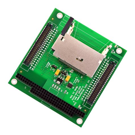
Table of contents
Other WinSystems Control Unit manuals