WinSystems PCM-A/D-16 User manual

OPERATIONS MANUAL
PCM-A/D-16
PCM-A/D-12
WinSystems reserves the right to make changes in the circuitry
and specifications at any time without notice.
© Copyright 1996 by WinSystems. All Rights Reserved.

REVISION HISTORY
P/N 403-0230-000
ECO Number Date Code Rev Level
Originated 960206 B
97-31 970513 B1
WinSystems- "The Embedded Systems Authority"

TABLE OF CONTENTS
SectionParagraph Page
Number Title Number
1General Information
1.1 Features1-1
1.2 General Description 1-1
1.3 Specifications1-2
2PCM-A/D Technical Reference
2.1Introduction2-1
2.2I/O Address Selection2-2
2.3Interrupt Routing2-2
2.4DC-DC Converter Selection 2-3
2.5Mode Selection2-3
2.6 Input Connector Pin Definitions2-8
2.7PC/104 Bus Pin Definitions2-8
2.8Connector/Jumper Summary 2-9
3PCM-A/D Programming Reference
3.1I/O Register Definitions 3-1
3.2Conversion Techniques 3-4
3.3 PCM-A/D Demonstration Program3-5
3.4Calibration Procedures3-7
APPENDIX A PCM-A/D Parts Placement Guide
APPENDIX B PCM-A/D Parts List
APPENDIX C BURR-BROWN ADS7806/ADS7807 Datasheet Reprint
APPENDIX D PCM-A/D Demo Software Source Listing
APPENDIX E PCM-A/D Schematic Diagrams

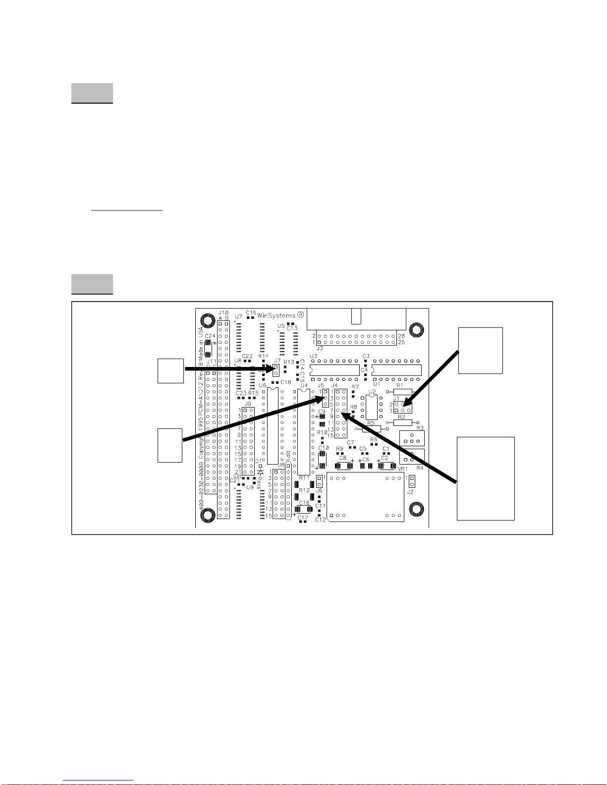
1GENERAL INFORMATION
1.1Features
nLow Power/Low Cost PC/104 A/D Converter Module
n16 Single ended or 8 Differential input channels
nAvailable in 12-Bit or 16-Bit models
n30uS Auto Conversion Time
nInterrupt available on end of conversion
nInput ranges of 0-5V and +/-10V
nOutput format in straight Binary or Signed two's complement Binary
nExtended industrial operating temperature range
nOptional DC/DC converter for +5V only operation
1.2General Description
The PCM-A/D-16 and PCM-A/D-12 are low cost, general purpose, successive approxi-
mation analog-to-digital converters. The PCM-A/D-16 uses the Burr-Brown ADS7807 16-
bit converter while the PCM-A/D-12 uses the Burr-Brown ADS7806 12-bit converter. Ap-
pendix C contains the datasheet reprints on these components.
The PCM-A/D supports 16 channels in a unipolar 5V range, or a bipolar +/-10 volt
range. Alternately 8 channels of differential input is supported in a 5 volt or 10 volt range.
Repetitive channel conversion time is 25uS and random channel access time is 30uS. The
endofconversioncanbedeterminedviasoftwarepollingorbyaninterrupttotheCPU.
970513PCM-A/D-12/16 OPERATIONS MANUALPage 1-1

1.3Specifications
1.3.1Electrical
Bus Interface : PCM-A/D-XX-8 PC/104 8-Bit stackthrough
PCM-A/D-XX-16 PC/104 16-Bit stackthrough
Power requirements :
+5V +/- 5% at 200mA typ. with DC-DC converter installed
15mA typ. w/o DC-DC converter installed
+12V +/-5% at 5mA typ. w/o DC-DC converter installed
-12V +/-5% at 5mA typ. w/o DC-DC converter installed
1.3.2Mechanical
Dimensions : 3.6" X 3.8" X 0.6"
PC Board :FR4 Epoxy glass with 2 signal layers and 2 power planes with screened
component legend and plated through holes.
Jumpers : 0.025" square posts on 0.10" centers.
Connectors : Analog input : 16-pin 0.10" grid RN type IDH-26-LP
1.3.3Environmental
Operating Temperature : -40° C to +85° C
Non-condensing relative humidity : 5% to 95%
Page 1-2PCM-A/D-12/16 OPERATIONS MANUAL970513
WinSystems- "The Embedded Systems Authority"

2PCM-A/D Technical Reference
2.1Introduction
Thissection of the manual is intended to providesufficient information regarding con-
figuration and usage of the PCM-A/D-16 and PCM-A/D-12 modules. WinSystems main-
tains a Technical Support Group to help answer questions regarding configuration and
programmingoftheboard.Foranswerstoquestionsnotadequatelyaddressedinthisman-
ual contact Technical Support at (817) 274-7553 between 8AM and 5PM Central Time.
Technical Support may also be requested by FAX at (817) 548-1358.
The PCM-A/D has 16 single-ended inputs or 8 differential inputs and converts in 25-
30uS. The end of conversion can be determined in any of three ways. A software timed de-
lay of 30-35uS can be used, the status register can be polled, or an end of conversion inter-
rupt can be used.
2.2I/O Address Selection
970513PCM-A/D-12/16 OPERATIONS MANUALPage 2-1
1 o o2
3 o o4
5 o o6
7 o o8
9 o o10
11 o o12
13 o o14
15 o o16
17o o18
19 o o20
21 o o22
1 o o2
3 o o4
5 o o6
7 o o8
9 o o10
11 o o12
13 o o14
15 o o16
J9
J8
I/O Address
Select Jumper J8
Interrupt Routing
Jumper J9

ThePCM-A/DusesfourconsecutiveI/Oaddresseswiththebaseaddressdeterminedby
thesetting of the jumperson J8.Each positiononthe J8jumper correspondsto anaddress
bit. A jumper installed matches a '0' in the address and a jumper left open matches a '1' in
the address. The illustration below shows the relationship between jumper positions and
address bits and also shows the correct jumpering for a base I/O address of 110H.
2.3Interrupt Routing
Theendof conversioninterrupt maybe routedto anyunusedPC/104interruptline us-
ing the jumper block at J9. The illustration below shows the relationship between the
jumper position and the interrupt selected. A sample jumpering for IRQ5 is also shown.
Page 2-2PCM-A/D-12/16 OPERATIONS MANUAL 970513
WinSystems- "The Embedded Systems Authority"
1 o o 2
3 o o4
5 o o6
7 o o8
9 o o10
11 o o12
13 o o14
15 o o16
A9
A8
A7
A6
A5
A4
A3
A2
J8
BASE I/O ADDRESS 110H
1 o o2
3 o o4
5 o o6
7 o o8
9 o o10
11 o o12
13 o o14
15 o o16
17o o18
19 o o20
21 o o22
IRQ15
IRQ14
IRQ12
IRQ11
IRQ10
IRQ7
IRQ6
IRQ5
IRQ4
IRQ3
IRQ2
J9
INTERRUPT ROUTING - IRQ5

2.4DC-DC Converter Selection
To allow for slightly better linearity across the full +/-10V input range supported, an
optionalDC-DCconverter is populated at VR1.When installed,it provides +15Vand -15V
to the analog circuitry. This allows the board to function with a +5 volt only supply.
Jumper blocks at J2 and J6 are jumpered to route the +12 and -12 volts from the PC/104
bus to the analog circuitry when the DC-DC converter is not installed.
WARNING :The J2and J6jumpersshould NEVERbeinstalled whentheDC-DCcon-
verterisinstalledordamagetothePCM-A/Dboard,otherPC/104modules,theCPUboard,
or the power supply may result. Boards provided with DC-DC converters from the factory
will not have the jumper posts installed at J2 and J6.
2.5Input Mode Selection
ThePCM-A/Disjumperselectableforoneof4inputmodes.Thesupportedmodesare.
1. 16 single-ended unipolar channels of 0-5V
2. 16 single-ended bipolar channels of +/-10V
3. 8 differential channels of 0-5V
4. 8 differential channels of +/-10V
970513 PCM-A/D-12/16 OPERATIONS MANUALPage 2-3
WinSystems- "The Embedded Systems Authority"
2 4 6
o o o
o o o
1 3 5
1 o o2
3 o o4
5 o o6
7 o o8
9 o o10
11 o o12
13 o o14
15 o o16
1 o
2 o
1 o
2 o
3 o
J7
J5
J1
J4
Mode configuration
jumpers J1, J4, J5, J7

2.5.1Mode 1- 0-5V Single-Ended Unipolar
This input mode provides for 16 channels of 0-5 volt input range. In no case should the
inputbedrivennegativeinthismode.Thecorrectjumperingforthismodeisshownbelow:
Each channel's input is delivered at J3. Refer to section 2.6 for input pin definitions.
When used in mode 1, binary values from 0 to FFF0H (FFFFH) are read from the con-
verter according to the following table.
Full Scale Range:0.0 - 5.0 Volts
Least Significant Bit (LSB) :76uV (16-Bit)
or 1.22mV (12-Bit)
+Full Scale (FS-1LSB) : 4.999924V (16-Bit)
or 4.99878V (12- Bit) FFFFH
Midscale : 2.50V 8000H
One LSB Below Midscale : 2.4999924V(16-Bit)
or 2.49878(12-Bit) 7FFFH
-Full Scale :0.0V 0000H
NOTE : On the PCM-A/D-12 the lower nibble of the hex value will always be 0.
Page 2-4PCM-A/D-12/16 OPERATIONS MANUAL970513
WinSystems- "The Embedded Systems Authority"
1 o o 2
3 o o 4
5 o o 6
7 o o 8
9 o o 10
11 o o 12
13 o o 14
15 o o 16
2 4 6
o o o
o o o
1 3 5
1 o
2 o
1 o
2 o
3o
J1J7J5J4
0-5 Volt - Single-Ended Mode

2.5.2 Mode 2- +/-10V Single-Ended Bipolar
Thisinputmode provides for16 channels of +-10Vinput range.The correctjumpering
for this mode is shown below :
Each channel's input is connected to J3. Refer to section 2.6 for input pin definitions.
When used in mode 2, two's complement binary values from 8000H to 7FFFH are read
from the converter according to the following table.
Full Scale Range :+/-10.0V
Least Significant bit :305uV (16-Bit)
or 4.88mV (12-Bit)
+Full Scale (FS-1LSB) : 9.999695V (16-Bit)
or 9.99512 (12-Bit) 7FFFH
Midscale : 0.0V 0000H
One LSB below Midscale : -305uV (16Bit)
or -4.88mV (12-Bit) FFFFH
-Full Scale :-10.0V 8000H
NOTE:On the PCM-A/D-12 the lower nibble of all hex values will be 0.
970513 PCM-A/D-12/16 OPERATIONS MANUALPage 2-5
WinSystems- "The Embedded Systems Authority"
1 o o 2
3 o o 4
5 o o 6
7 o o 8
9 o o 10
11 o o 12
13 o o 14
15 o o 16
2 4 6
o o o
o o o
1 3 5
1 o
2 o
1 o
2 o
3o
J1J7J5J4
+/-10 Volt - Single Ended Bipolar Mode

2.5.3Mode 3- 0-5V Differential
Thisinputmode providesfor 8channels of0-5volt differentialinput.Thecorrectjump-
ering for this mode is shown below :
Each channel's input is connected to J3. Refer to section 2.6 for the input pin defini-
tions.
When used in mode 3, binary values range from 0 to FFFFH as shown in the following
table.
Full Scale Range : 0.0 - 5.0 Volts
Least Significant Bit (LSB) : 76uV (16-Bit)
or 1.22mV (12-Bit)
+Full Scale (FS-1LSB) : 4.999924V(16-Bit)
or 4.99878V (12- Bit) FFFFH
Midscale : 2.50V 8000H
One LSB Below Midscale : 2.4999924V(16-Bit)
or 2.49878(12-Bit) 7FFFH
-Full Scale 0.0V 0000H
NOTE : On the PCM-A/D-12 the lower nibble of the hex value will always be 0.
Page 2-6PCM-A/D-12/16 OPERATIONS MANUAL970513
WinSystems- "The Embedded Systems Authority"
1 o o 2
3 o o 4
5 o o 6
7 o o 8
9 o o 10
11 o o 12
13 o o 14
15 o o 16
2 4 6
o o o
o o o
1 3 5
1 o
2 o
1 o
2 o
3o
J1J7J5J4
0-5 Volt - Differential Mode

2.5.4 Mode 4- +/-10 Volt differential/Bipolar
This mode provides 8 channels of differential input with 2 important limitations.
1. The maximum differential voltage between the two legs is 10V.
2. Neither input leg can be, as referenced to ground, greater than +10V nor less than -10V.
The jumpering for this mode is as shown below :
Eachchannel'sinput voltage is applied toJ3as referenced insection 2.6. Be sureto use
the differential pin definitions when using this mode.
Two's complement binary values are read from the converter per the following table.
Full Scale Range :+/-10.0V
Least Significant bit :305uV (16-Bit)
or 4.88mV (12-Bit)
+Full Scale (FS-1LSB) : 9.999695V (16-Bit)
or 9.99512 (12-Bit) 7FFFH
Midscale : 0.0V 0000H
One LSB below Midscale : -305uV (16Bit)
or -4.88mV (12-Bit) FFFFH
-Full Scale :-10.0V 8000H
NOTE:On the PCM-A/D-12 the lower nibble of all hex values will be 0.
970513PCM-A/D-12/16 OPERATIONS MANUALPage 2-7
WinSystems- "The Embedded Systems Authority"
1 o o 2
3 o o 4
5 o o 6
7 o o 8
9 o o 10
11 o o 12
13 o o 14
15 o o 16
2 4 6
o o o
o o o
1 3 5
1 o
2 o
1 o
2 o
3o
J1J7J5J4
+/-10 Volt - Differential/Bipolar Mode

2.6Input Connector Pin definitions
Input to the PCM-A/D board is made via J3. When used in the single-ended mode, 16-
channelsare available and when used in a differential mode, 8 channels are available. The
illustration below shows the pin definitions for each case.
2.7PC/104 Bus Pin Definitions
The PC/104 connectors at J10 and J11 are shown here with the signal designations.
Page 2-8PCM-A/D-12/16 OPERATIONS MANUAL970513
WinSystems- "The Embedded Systems Authority"
1 o o 2
3 o o4
5 o o6
7 o o8
9 o o10
11 o o12
13 o o14
15 o o16
17 o o18
19 o o20
21o o 22
23 o o24
25 o o26
1 o o 2
3 o o4
5 o o6
7 o o8
9 o o10
11 o o12
13 o o14
15 o o16
17 o o18
19 o o20
21o o 22
23 o o24
25 o o26
CH0
CH1
GND
CH2
GND
CH3
GND
CH4
GND
CH5
GND
CH6
CH7
CH8
CH9
GND
CH10
GND
CH11
GND
CH12
GND
CH13
GND
CH14
CH15
CH0+
CH1+
GND
CH2+
GND
CH3+
GND
CH4+
GND
CH5+
GND
CH6+
CH7+
CH0-
CH1-
GND
CH2-
GND
CH3-
GND
CH4-
GND
CH5-
GND
CH6-
CH7-
J3J3
Single-Ended Input Channels Differential Input Channels
B1 o o A1
B2 o o A2
B3 o o A3
B4 o o A4
B5 o o A5
B6 o o A6
B7 o o A7
B8 o o A8
B9 o o A9
B10 o o A10
B11 o o A11
B12 o o A12
B13 o o A13
B14 o o A14
B15 o o A15
B16 o o A16
B17 o o A17
B18 o o A18
B19 o o A19
B20 o o A20
B21 o o A21
B22 o o A22
B23 o o A23
B24 o o A24
B25 o o A25
B26 o o A26
B27 o o A27
B28 o o A28
B29 o o A29
B30 o o A30
B31 o o A31
B32 o o A32
C0 o o D0
C1 o oD1
C2 o o D2
C3 o o D3
C4 o o D4
C5 o o D5
C6 o o D6
C7 o o D7
C8 o o D8
C9 o o D9
C10 o o D10
C11 o o D11
C12 o o D12
C13 o o D13
C14 o o D14
C15 o o D15
C16 o o D16
C17 o o D17
C18 o o D18
C19 o o D19
GND
RESET
+5V
IRQ9
-5V
DRQ2
-12V
0WS
+12V
GND
MEMW
MEMR
IOW
IOR
DACK3
DRQ3
DACK1
DRQ1
REFRESH
SYSCLK
IRQ7
IRQ6
IRQ5
IRQ4
IRQ3
DACK2
TC
BALE
+5V
OSC
GND
GND
IOCHK
BD7
BD6
BD5
BD4
BD3
BD2
BD1
BD0
IOCHRDY
AEN
SA19
SA18
SA17
SA16
SA15
SA14
SA13
SA12
SA11
SA10
SA9
SA8
SA7
SA6
SA5
SA4
SA3
SA2
SA1
SA0
GND
GND
SBHE
LA23
LA22
LA21
LA20
LA19
LA18
LA17
MEMR
MEMW
SD8
SD9
SD10
SD11
SD12
SD13
SD14
SD15
KEY
GND
MEMCS16
IOCS16
IRQ10
IRQ11
IRQ12
IRQ15
IRQ14
DACK0
DRQ0
DACK5
DRQ5
DACK6
DRQ6
DACK7
DRQ7
+5V
MASTER
GND
GND

2.8Connector/Jumper Summary
Connector/DescriptionPage
Jumper Reference
J1 Mode Select, differential or single-ended 2-3
J2DC-DC Converter Enable2-3
J3Analog input connector 2-8
J4Input range select jumper 2-3
J5Mode select, differential vs. single-ended2-3
J6DC-DC Converter Enable2-3
J7Mode Select, binary vs. two's complement2-3
J8I/O Address Select 2-2
J9Interrupt Routing Select2-2
J10PC/104-8 Connector2-8
J11PC/104-16 Connector2-8
970513 PCM-A/D-12/16 OPERATIONS MANUAL Page 2-9
WinSystems- "The Embedded Systems Authority"

3PCM-A/D Programming Reference
3.1I/O Register Definitions
The PCM-A/D uses 4 consecutive I/O addresses beginning with a base address selected
viajumperblockJ8.SeeSection2.1forI/Oaddressselectiondetails.ThefourallocatedI /O
addresses are used as shown here :
ADDRESSWrite RegisterRead Register
—————————————————————————————————————-
BASEChannel SelectStatus Register
BASE+1 Channel Select/Conversion StartLSB Data
BASE+2 Conversion Start Only MSB Data
BASE+3 Reserved Reserved
Each Register will be examined in more detail.
3.1.1Base Address
Write Register - Channel Select
D7 - N/A
D6 - N/A
D5 - N/A
D4 - N/A
D3 - Bit 3 of select nibble
D2 - Bit 2 of select nibble
D1 - Bit 1 of select nibble
D0 - Bit 0 of select nibble
WritingavaluetotheBASEI/Oportwillcausetheonboardmultiplexerstoselectanew
inputchannel.The channelnumber selectedisthebinaryvalue ofthelower4 bits.Nocon-
versionisstartedand adelayofapproximately6uS formultiplexer settlingis requiredbe f-
ore beginning a conversion.
970513 PCM-A/D-12/16 OPERATIONS MANUAL Page 3-1

Read Register - Conversion Status
D7 - N/A
D6 - N/A
D5 - N/A
D4 - N/A
D3 - N/A
D2 - N/A
D1 - Busy 0 = Converter busy, 1 = Conversion complete
D0 - Interrupt 0 = Conversion in progress, 1 = Conversion complete
This status register indicates when a conversion is complete. It is recommended that
software routines wait until both the Conversioncomplete and the Interrupt bits are both
set before reading the conversion data.
3.1.2 Base + 1 Address
Write Register - Select Channel/Start Conversion
D7 - N/A
D6 - N/A
D5 - N/A
D4 - N/A
D3 - Bit 3 of select nibble
D2 - Bit 2 of Select nibble
D1 - Bit 1 of select nibble
D0 - Bit 0 of select nibble
Writingavalue totheBASE +1I/O addressnotonlyselectsthechannelnumberasen-
coded in bits 3-0 but after a hardware settling delay of approximately 6uS starts a conver-
sion. This is the normal method to begin a conversion as the channel selection and
conversion start are automated into a single write.
Read Register - LSB Data
D7 - D7 of conversion data
D6 - D6 “ ” “
D5 - D5 “ ” “
D4 - D4 “ ” “
D3 - D3 “ ” “
D2 - D2 “ ” “
D1 - D1 “ ” “
D0 - D0 “ ” “
Reading of I/O base address + 1 will present the lower 8-bits of the 16-bit conversion
data. Note that on the 12-Bit converter module,thelower 4bits ofthis register willalways
read as 0. This allows software to transparently use either the 12-bit or the 16-bit module .
Page 3-2PCM-A/D-12/16 OPERATIONS MANUAL 970513
WinSystems- "The Embedded Systems Authority"

Notethat thedata isonly validif boththe BUSYand INTERRUPT bitsareboth set to 1 in
the status register.
3.1.3Base + 2 Address
Write Register - Start Conversion
D7 = N/A
D6 = N/A
D5 = N/A
D4 = N/A
D3 = N/A
D2 = N/A
D1 = N/A
D0 = N/A
AwritetothisregisterwithanyvaluewillstarttheA/Dconverteronwhateverchannel
waspreviouslyselectedbytheChannelSelectRegisterortheChannelSelect/StartConver -
sionregister.Thismethodofstartingtheconverterallowsformaximumthroughputwhen
repetitively converting on the same channel as no multiplexer settling time is required.
Read Register - MSB Data
D7 = D15 of conversion data
D6 = D14 “ ” “
D5 = D13 “ ” “
D4 = D12 “ ” “
D3 = D11 “ ” “
D2 = D10 “ ” “
D1 = D9 “ ” “
D0 = D8 “ ” “
Readingfromthisregistergivestheupper8-bitsofthe16-bitconversiondata.Thisdata
is only valid if both the BUSY and INTERRUPT bits are set to 1 in the status register.
970513PCM-A/D-12/16 OPERATIONS MANUALPage 3-3
WinSystems- "The Embedded Systems Authority"

3.2Conversion Techniques
The PCM-A/D can be programmed in any language supporting port I/O instructions.
Thecodesnippetbelowisinthe'C'languageanddemonstratesasimplefunctionthattakes
asan argument the channel number and returns a 16-bit unsigned value corresponding to
thecurrentconversionvalue.Thenextsectiondescribesasample/test/calibrationprogram
included with the PCM-A/D board both in executable and source form.
#define BASE_ADDRESS 0x110
unsigned convert(int channel_number)
{
unsigned return_value;
/* Start the conversion by writing to the Select/Start conversion Register */
outportb(BASE_ADDRESS + 1, channel_number);
/* Now wait for the conversion to complete */
while((inportb(BASE_ADDRESS) & 0x03) != 3)
;
/* Now read out the 2 bytes that make up the value */
return_value = inportb(BASE_ADDRESS + 2);
/* Shift the MSB value up 8 bits in preparation for the LSB */
return_value = return_value < 8;
/* Read the LSB value and 'OR' it into the prepared MSB value */
return_value = return_value | inportb(BASE_ADDRESS + 1);
return return_value;
}
Page 3-4PCM-A/D-12/16 OPERATIONS MANUAL 970513
WinSystems- "The Embedded Systems Authority"

3.3PCM-A/D Demonstration Program
Included on a 3 1/2" diskette with the PCM-A/D board is a sample program in both 'C'
sourcecodeand inMS-DOS executableformat. ThePCMAD12.EXE filewascreatedusing
Borland C/C++ Version 3.1. This demo program may be used as a diagnostic/calibration
programorportionsofitssourcecodemaybeusedinauser'sapplicationprogram.Thepro-
gram's source code demonstrates both interrupt driven and polled-mode converter tech-
niques. PCMAD12.EXE is executed from the MS-DOS command line with:
PCMAD12 <Enter>
Ascreendisplaylikethatshownbelowshouldbedisplayedandtheinterruptcounterin
the lower right corner should be counting conversions.
NOTE: ThePCMAD12.EXEprogramassumesthatabaseaddressof110Hhasbeense-
lected and the IRQ5 is also selected. Refer to Section 2 of this manual for hardware selec-
tion details.
970513PCM-A/D-12/16 OPERATIONS MANUALPage 3-5
WinSystems- "The Embedded Systems Authority"
Channel RAW HIGH LOW DATA CURRENT MAX MIN VOLTA GE
Number DATA DATA DATA DEV. VOLTAGE VOLTAGE VOLTAGE DEVIATION
——————————————————————————-—————————————————-
00 FFFF FFFF FFFF 0000 5.0000 5.0000 5.0000 0.0000
01 FFFF FFFF FFFF 0000 5.0000 5.0000 5.0000 0.0000
02 FFFF FFFF FFFF 0000 5.0000 5.0000 5.0000 0.0000
03 FFFF FFFF FFFF 0000 5.0000 5.0000 5.0000 0.0000
04 FFFF FFFF FFFF 0000 5.0000 5.0000 5.0000 0.0000
05 FFFF FFFF FFFF 0000 5.0000 5.0000 5.0000 0.0000
06 FFFF FFFF FFFF 0000 5.0000 5.0000 5.0000 0.0000
07 FFFF FFFF FFFF 0000 5.0000 5.0000 5.0000 0.0000
08 FFFF FFFF FFFF 0000 5.0000 5.0000 5.0000 0.0000
09 FFFF FFFF FFFF 0000 5.0000 5.0000 5.0000 0.0000
10 FFFF FFFF FFFF 0000 5.0000 5.0000 5.0000 0.0000
11 FFFF FFFF FFFF 0000 5.0000 5.0000 5.0000 0.0000
12 FFFF FFFF FFFF 0000 5.0000 5.0000 5.0000 0.0000
13 FFFF FFFF FFFF 0000 5.0000 5.0000 5.0000 0.0000
14 FFFF FFFF FFFF 0000 5.0000 5.0000 5.0000 0.0000
15 FFFF FFFF FFFF 0000 5.0000 5.0000 5.0000 0.0000
—————————————————————————---—————————————————
'T' Toggle Scale, 'B' Converter toggle 'M' Interrupt Mode toggle, 'R' Reset Values
————————————————————---——————————————————————-
Scale : +0 to +5 Volts - Single-Ended 12-Bit Interrupt Mode 34256

There are 5 keystrokes recognized by PCMAD12.EXE. They are as follows :
'T'- Toggles the input mode through the 4 supported modes :
+0 to +5 Volts - Single Ended
-10 to +10 Volts - Single Ended
+0 to +5 Volts - Differential
-10 to +10 Volts - Differential
NOTE :Pressing'T'onlychangesthesoftware'sinterpretationofthemodebeingused.
The values displayed will be meaningless in any mode except for the one for which the
board has been jumpered for.
'B' - Toggles the converter type between 12-bit and 16-bit.
'M' - Toggle the conversion mode
This key toggles the conversion mode between “Interrupt Mode” and “Polled Mode”.
When in the “InterruptMode” a counter inthe lower right corner will display the number
of interrupts received since the last 'M', 'T', or 'R' command.
'R'- Reset Values
Pressing the 'R' key resets the High, Low and Deviation values to 0. This may be desir-
ableafterchangingmodesorinputvoltagestocheckthestabilityofthePCM-A/Dorthein-
put source.
'ESCAPE'- Exit to DOS
Pressing 'ESCAPE'will unhook the current interrupt vectors and return the system to
the DOS prompt.
Page 3-6PCM-A/D-12/16 OPERATIONS MANUAL 970513
WinSystems- "The Embedded Systems Authority"
This manual suits for next models
1
Table of contents
Popular Media Converter manuals by other brands

Honeywell
Honeywell 04200-A-1201 operating instructions

AlienTech
AlienTech Powergate3+ Instruction manual and users guide

Balanced Audio Technology
Balanced Audio Technology REX DAX owner's manual

Solid State Logic
Solid State Logic Alpha-Link AX user guide

FONESTAR
FONESTAR FS-2915CDR instruction manual

Clarke
Clarke 40590A Operator's manual