Xycom XEMBEDDED XCPC-9200 User manual

XCPC-9200
Conduction Cooled/Air Cooled Dual PMC Carrier
retired

2009 X
EMBEDDED
™, LLC. (XycomVME, Inc.) Printed in the United States of America
Revision Description Date
A Init 05/09
B Reviewed and released 06/09
Part Number 649200
Trademark Information
Brand or product names are trademarks or registered trademarks of their respective owners.
Intel and Core 2 Duo, Core Duo, Pentium M, Pentium and Celeron are trademarks of Intel Corporation.
Windows, Windows NT, Windows 2000, Windows XP, Windows 7 are registered trademarks of
Microsoft Corporation in the US and in other countries.
Copyright Information
This document is copyrighted by Xembedded, LLC (A XycomVME company, formally Xycom) and
shall not be reproduced or copied without expressed written authorization from Xembedded.
The information contained within this document is subject to change without notice. Xembedded does not
guarantee the accuracy of the information.
WARNING
This is a Class A product. In a domestic environment this product may cause radio interference, in which case
the user may be required to take adequate measures.

XCPC-9200
1
XCPC-9200..................................................................................................................................i
About This Manual....................................................................................................................3
Feedback .............................................................................................................................................3
References...........................................................................................................................................3
Chapter 1 General Description.................................................................................................4
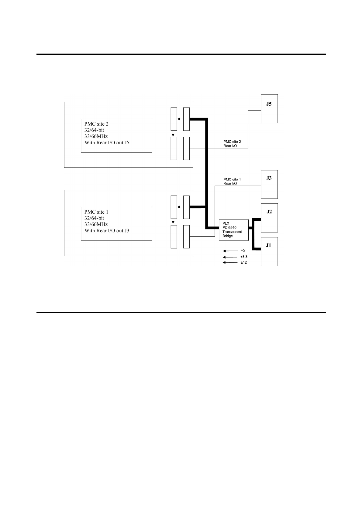
Figure 1-1 below shows the Architectural of the board.......................................................................6
PMC Interface .....................................................................................................................................6
CompactPCI Interface........................................................................................................................11
CompactPCI Connector Keying.......................................................................................................11
PCI Bus interface............................................................................................................................12
Specifications....................................................................................................................................12
Safety:.............................................................................................................................................12
EMC...............................................................................................................................................12
Chapter 2 Installation Guide Introduction.............................................................................13
XCPC-9200 Rear I/O.........................................................................................................................13
CompactPCI Interface Connector Pin Definitions...............................................................................14
CompactPCI Interface J1 Pin-out.....................................................................................................14
CompactPCI Interface J2 Pin-out.....................................................................................................15
CompactPCI Interface J3 Pin-out.....................................................................................................16
CompactPCI Interface J5 Pin-out.....................................................................................................17
Installation into rack..........................................................................................................................18
XCPC-9200 Mechanical Description .................................................................................................19
Jumper Settings and Locations...........................................................................................................21
Carrier PMC PCI clock speed..........................................................................................................21
Fault Indicators ............................................................................................................................... 22

XCPC-9200
2
European Union Directive 89/336/EEC requires that this apparatus comply with relevant ITE EMC standards.
EMC compliance demands that this apparatus is installed within a CompactPCI enclosure designed to contain
electromagnetic radiation and which will provide protection for the apparatus with regard to electromagnetic
immunity. This enclosure must be fully shielded. An example of such an enclosure is a 6U EMC-RFI
CompactPCI System chassis, which includes a front cover to complete the enclosure.
The connection of non-shielded equipment interface cables to this equipment will invalidate European Free
Trade Area (EFTA) EMC compliance and may result in electromagnetic interference and/or susceptibility
levels that are in violation of regulations which apply to the legal operation of this device. It is the
responsibility of the system integrator and/or user to apply the following directions, as well as those in the
user manual, which relate to installation and configuration:
All interface cables should be shielded, both inside and outside of the CompactPCI enclosure.
Braid/foil type shields are recommended for serial, parallel, and SCSI interface cables. Where
as external mouse cables are not generally shielded, an internal mouse interface cable must
either be shielded or looped (1 turn) through a ferrite bead at the enclosure point of exit
(bulkhead connector). External cable connectors must be metal with metal back-shells and
provide 360-degree protection about the interface wires. The cable shield must be terminated
directly to the metal connector shell; shield ground drain wires alone are not adequate.
CompactPCI panel mount connectors that provide interface to external cables (e.g.,
RS232, USB, keyboard, mouse, etc.) must have metal housings and provide direct connection
to the metal CompactPCI chassis. Connector ground drain wires are not adequate.

XCPC-9200
3
About This Manual
The Xembedded reference manual provides functional, architectural, and mechanical descriptions
of the XCPC-9200. This manual is intended for anyone who designs OEM products which have
requirements for a Dual PMC Carrier that require large amounts of power on each PMC site.
Xembedded LLC - Manufacturer of Xycom VME and embedded products! Whether you
are using VMEbus, CompactPCI bus or PMC bus; Xembedded has a product to fit your
rugged and industrial application. Don't see what you need? We do custom products
leveraging our years of experience and base product designs.
Feedback
Xembedded welcomes feedback on how we can make our manuals and technical documentation
more useful to our customers. Please feel free to send comments and suggestions to
suppo[email protected].
References
PICMG 2.0 R3.0 ECN2.0-3.0-002
PICMG 2.3 R1.0
PICMG 2.6
PICMG
c/o Virtual, Inc.
401 Edgewater Place, Suite 600
Wakefield, MA 01880, USA
Phone: 1-781-246-9318
(8:00am to 5:00pm Eastern US time)
Fax: 1-781-224-1239
Email: info@picmg.org
Xembedded Incorporated
1050 Highland Dr..
Ann Arbor, MI 48108
Phone: 1-734-975-0577
Email: Sales@xembedded.com

XCPC-9200
4
Chapter 1 General Description
The XCPC-9200 is the most advanced CompactPCI (cPCI) carrier in the market that offers
two IEEE.1-2201-compliant conduction-cooled PMC sites with 25 watts of power to each
site.
Conduction-cooled module that is also available as an air cooled module.
High current/wattage power supply to deliver up to 25 watts of power to each
PMC site.
64/32-bit, 133/66/33MHz PCI bus on the CompactPCI bus. The PMC side
supports 64/32-bit operation at 133MHz or 66MHz speeds (user selectable).
It supports the interrupts INTA, INTB, INTC, and INTD.
CompactPCI I/O signaling is auto-configured and supports both 3.3V and 5V
backplanes. The PMC interfaces support 3.3V I/O signaling only.
The PMC connectors on the carrier include all the signals of a 66/33 MHz,
64/32-bit, multi-master PCI bus, the power rails for 3.3V, 5V, V(I/O) and other
specialized signals for board detection.
Each PMC site provides full rear I/O capability through its J14/J24 connector.
The rear I/O is routed through the J3 and J5 connectors on the backplane.
A PCI-to-PCI bridge provides for coupling of the PMC sites to the
CompactPCI backplane, so that two independent PCI busses exist. The
CompactPCI interface is the PLX PCI6540 PCI-to-PCI bridge. It is software
transparent and consequently a software driver is not required to manage
data transfer between the PMC module and the CompactPCI bus.
The XCPC-9200 has been designed to function with all CompactPCI
backplanes.
The J4 connector is not present on the XCPC_9200 so this carrier module
can also be used in systems employing an H110 backplane.

XCPC-9200
5
Versions of the XCPC-9200
The conduction cooled version of the XCPC-9200 module uses a custom
conduction cooled assembly consisting of a conduction cooled frame, thermo bars,
ejector/injectors and Wedge-Loks
®
designed to thermally conduct heat away from
the conduction-cooled PMC modules per ANSI/VITA 30.1-2001. In a conduction-
cooled assembly, adequate thermal conduction must be provided to prevent a
temperature rise above the maximum operating temperature. This version of the
XCPC-9200 is design for use in an ATR type chassis.
The XCPC-9200 is also available in an extended temperature version which uses a
standard CompactPCI 6U front panel shown in Fig. 2-2.
The air cooled XCPC-9200 requires adequate air circulation (200 to 300LFM) to
prevent a temperature rise above the maximum operating temperature and to
prolong the life of the electronics. If the installation is in an industrial environment
and the board is exposed to environmental air, careful consideration should be
given to air filtering.

XCPC-9200
6
Figure 1-1 below shows the Architectural of the board.
PMC Interface
The two single-width PMC slots on the XCPC-9200 provide an easy way to extend a
CompactPCI system. PMC double-wide modules can also be used on the XCPC-9200.
PMC modules are available in a wide range of interfaces and functions available from a
large number of PMC vendors.
The secondary (PMC) side of the PCI-to-PCI bridge provides a 32/64-bit wide PCI data
path for speeds up to 133 MHz (PCI-X), which is routed to the onboard connectors Jn1,
Jn2 and Jn3. These connectors also provide the power for the PMC module. The PMC
slots have been designed to comply with the IEEE 1386.1 specification, which defines the
PCI electrical interface for the CMC (Common Mezzanine Card) form factor.

XCPC-9200
7
Fig 1-2 PMC connector layout

XCPC-9200
8
Table 1-1 PMC 1 and PMC 2 Connector Pin Out
Connectors J11 and J21 Connectors J12 and J22
Signal PIN
PIN
Signal Signal PIN
PIN
Signal
TCK 1 2 -12V +12V 1 2 TRST*
Ground 3 4 INTA* TMS 3 4 TDO
INTB* 5 6 INTC* TDI 5 6 Ground
BUSMODE1*
7 8 +5V Ground 7 8 PCI-RSVD*
INTD* 9 10 PCI-RSVD*
PCI-RSVD* 9 10 PCI-RSVD*
Ground 11 12 PCI-RSVD*
BUSMODE2*
11 12 +3.3V
CLK 13 14 Ground RST* 13 14 BUSMODE3*
Ground 15 16 GNT* +3.3V 15 16 BUSMODE4*
REQ* 17 18 +5V PCI-RSVD* 17 18 Ground
V(I/O) 19 20 AD(31) AD(30) 19 20 AD(29)
AD(28 21 22 AD(27) Ground 21 22 AD(26)
AD(25) 23 24 Ground AD(24) 23 24 +3.3V
Ground 25 26 C/BE(3)* IDSEL 25 26 AD(23)
AD(22) 27 28 AD(21) +3.3V 27 28 AD(20)
AD(19) 29 30 +5V AD(18) 29 30 Ground
V(I/O) 31 32 AD(17) AD(16) 31 32 C/BE(2)*
FRAME* 33 34 Ground Ground 33 34 PMC-RSVD
Ground 35 36 IRDY* TRDY* 35 36 +3.3V
DEVSEL* 37 38 +5V Ground 37 38 STOP*
Ground 39 40 LOCK* PERR* 39 40 Ground
SDONE* 41 42 SBO* +3.3V 41 42 SERR*
PAR 43 44 Ground C/BE(1)* 43 44 Ground
V(I/O) 45 46 AD(15) AD(14) 45 46 AD(13)
AD(12) 47 48 AD(11) M66EN 47 48 AD(10)
AD(09) 49 50 +5V AD(08) 49 50 +3.3V
Ground 51 52 C/BE(0)* AD(07) 51 52 PMC-RSVD
AD(06) 53 54 AD(05) +3.3V 53 54 PMC-RSVD
AD(04) 55 56 Ground PMC-RSVD 55 56 Ground
V(I/O) 57 58 AD(03) PMC-RSVD 57 58 PMC-RSVD
AD(02) 59 60 AD(01) Ground 59 60 PMC-RSVD
AD(00) 61 62 +5V ACK64* 61 62 +3.3V
Ground 63 64 REQ64* Ground 63 64 PMC-RSVD

XCPC-9200
9
Table 1-2 PMC 1 and PMC 2 J13 and J23 Connector Pin Out
Connectors J13 and J23
Signal PIN PIN Signal
PCI-RSVD 1 2 Ground
Ground 3 4 C/BE(7)*
C/BE(6)* 5 6 C/BE(5)*
C/BE(4)* 7 8 Ground
V(I/O) 9 10 PAR64
AD(63) 11 12 AD(62)
AD(61) 13 14 Ground
Ground 15 16 AD(60)
AD(59) 17 18 AD(58)
AD(57) 19 20 Ground
V(I/O) 21 22 AD(56)
AD(55) 23 24 AD(54)
AD(53) 25 26 Ground
Ground 27 28 AD(52)
AD(51) 29 30 AD(50)
AD(49) 31 32 Ground
Ground 33 34 AD(48)
AD(47) 35 36 AD(46)
AD(45) 37 38 Ground
V(I/O) 39 40 AD(44)
AD(43) 41 42 AD(42)
AD(41) 43 44 Ground
Ground 45 46 AD(40)
AD(39) 47 48 AD(38)
AD(37) 49 50 Ground
Ground 51 52 AD(36)
AD(35) 53 54 AD(34)
AD(33) 55 56 Ground
V(I/O) 57 58 AD(32)
PCI-RSVD 59 60 PCI_RSVD
PCI-RSVD 61 62 Ground
Ground 63 64 PCI-RSVD

XCPC-9200
10
Table 1-3 PMC 1 and PMC 2 Connector Pin Out
Connectors J14 Connectors J24
Signal PIN
PIN
Signal Signal PIN PIN Signal
PMC1I/O-1 1 2 PMC1I/O-2 PMC2 I/O-1 1 2 PMC2 I/O-2
PMC1I/O-3 3 4 PMC1I/O-4 PMC2 I/O-3 3 4 PMC2 I/O-4
PMC1I/O-5 5 6 PMC1I/O-6 PMC2 I/O-5 5 6 PMC2 I/O-6
PMC1I/O-7 7 8 PMC1I/O-8 PMC2 I/O-7 7 8 PMC2 I/O-8
PMC1I/O-9 9 10 PMC1I/O-10
PMC2 I/O-9 9 10 PMC2 I/O-10
PMC1I/O-11
11 12 PMC1I/O-12
PMC2 I/O-11 11 12 PMC2 I/O-12
PMC1I/O-13
13 14 PMC1I/O-14
PMC2 I/O-13 13 14 PMC2 I/O-14
PMC1I/O-15
15 16 PMC1I/O-16
PMC2 I/O-15 15 16 PMC2 I/O-16
PMC1I/O-17
17 18 PMC1I/O-18
PMC2 I/O-17 17 18 PMC2 I/O-18
PMC1I/O-19
19 20 PMC1I/O-20
PMC2 I/O-19 19 20 PMC2 I/O-20
PMC1I/O-21
21 22 PMC1I/O-22
PMC2 I/O-21 21 22 PMC2 I/O-22
PMC1I/O-23
23 24 PMC1I/O-24
PMC2 I/O-23 23 24 PMC2 I/O-24
PMC1I/O-25
25 26 PMC1I/O-26
PMC2 I/O-25 25 26 PMC2 I/O-26
PMC1I/O-27
27 28 PMC1I/O-28
PMC2 I/O-27 27 28 PMC2 I/O-28
PMC1I/O-29
29 30 PMC1I/O-30
PMC2 I/O-29 29 30 PMC2 I/O-30
PMC1I/O-31
31 32 PMC1I/O-32
PMC2 I/O-31 31 32 PMC2 I/O-32
PMC1I/O-33
33 34 PMC1I/O-34
PMC2 I/O-33 33 34 PMC2 I/O-34
PMC1I/O-35
35 36 PMC1I/O-36
PMC2 I/O-35 35 36 PMC2 I/O-36
PMC1I/O-37
37 38 PMC1I/O-38
PMC2 I/O-37 37 38 PMC2 I/O-38
PMC1I/O-39
39 40 PMC1I/O-40
PMC2 I/O-39 39 40 PMC2 I/O-40
PMC1I/O-41
41 42 PMC1I/O-42
PMC2 I/O-41 41 42 PMC2 I/O-42
PMC1I/O-43
43 44 PMC1I/O-44
PMC2 I/O-43 43 44 PMC2 I/O-44
PMC1I/O-45
45 46 PMC1I/O-46
PMC2 I/O-45 45 46 PMC2 I/O-46
PMC1I/O-47
47 48 PMC1I/O-48
PMC2 I/O-47 47 48 PMC2 I/O-48
PMC1I/O-49
49 50 PMC1I/O-50
PMC2 I/O-49 49 50 PMC2 I/O-50
PMC1I/O-51
51 52 PMC1I/O-52
PMC2 I/O-51 51 52 PMC2 I/O-52
PMC1I/O-53
53 54 PMC1I/O-54
PMC2 I/O-53 53 54 PMC2 I/O-54
PMC1I/O-55
55 56 PMC1I/O-56
PMC2 I/O-55 55 56 PMC2 I/O-56
PMC1I/O-57
57 58 PMC1I/O-58
PMC2 I/O-57 57 58 PMC2 I/O-58
PMC1I/O-59
59 60 PMC1I/O-60
PMC2 I/O-59 59 60 PMC2 I/O-60
PMC1I/O-61
61 62 PMC1I/O-62
PMC2 I/O-61 61 62 PMC2 I/O-62
PMC1I/O-63
63 64 PMC1I/O-64
PMC2 I/O-63 63 64 PMC2 I/O-64
Note: The PMC rear I/O signals from Jn4 (CON8 and CON12) are routed to CompactPCI
connectors J3 and J5, the pin-out for which is described later in this chapter.

XCPC-9200
11
CompactPCI Interface
The XCPC-9200 utilizes a PLX PCI6540 chip for its interface to the cPCI back plane. The chip is a
high-performance asynchronous 133MHz, 64-bit PCI-X to PCI-X bridge. The XCPC-9200 runs in
transparent mode. All bus signals are provided on the CompactPCI connectors J1 and J2 (64-bit
extension). The XCPC-9200 meets the requirements of the interface definition of the CompactPCI
Specification PICMG 2.1 R1.0, a consequence of which is that the CompactPCI interface of the
board will be pre-charged when the board is plugged into a running system. The complete
CompactPCI connector configuration comprises four connectors named J1, J2, J3, and J5. Their
functions are as follows:
• J1 and J2: 64-bit CompactPCI interface with PCI bus signals, arbitration,
clock, and power.
• J3 and J5 provide rear I/O interface functionality from the PMC module.
CompactPCI Connector Keying
CompactPCI connectors support guide keys to ensure a correct polarized mating. A proper mating
is further assured by the use of color coded keys for 3.3V and 5V operation.
Color coded keys prevent inadvertent installation of a 5V peripheral board into a 3.3V slot. The
XCPC-9200 module will work in both 3.3V and 5V systems. Backplane connectors are always
keyed according to the signaling (VIO) level to prevent plugging a CompactPCI connector into the
wrong backplane slot, although with the XCPC-9200 this is not a problem due to the dual I/O
voltage support within the PLX PCI6540.
Coding key colors on J1 are defined as followed:
Signal Voltage Key Color
3.3V
Cadmium Yellow
5V Brilliant Blue

XCPC-9200
12
Main Features
PCI Bus interface
The XCPC-9200 uses the PLX-6540 bridge for the PCI-X bus interface to the cPCI bus. The
bridge has the following features:
•PCI R2.3 capable
•PICMG 2.1 Hot swappable
•PCIX 64-bit, 33MHz to 133Mhz PCI clock speed
•Asynchronous operation across the primary (Compact PCI backplane) and secondary
(PMC sites) interfaces. This allows the two interfaces to run at two different speeds.
•10KB FIFO
•Transparent mode operation.
•Support for 8 Bus Masters
Specifications
The following table is the XCPC-9200 Specifications, showing the recommended operating conditions.
Condition Recommendation
Compliance PCI R2.3, PICMG 2.0, PICMG 2.1,
Air Flow 200LFM with no PrPMC/PMC installed (air flow is mostly
driven by the PMC requirements)
Power Each PMC site is capable of sourcing 25 watts of power;
the carrier alone requires 2 watts.
Dimensions Height-233 mm, Depth- 160 mm, Width – 20.27 mm
Operating Temperature -40 to 85° C
Storage Temperature -55 to 105° C
Relative Humidity 5-95% Non-Condensing
Shock 40g
Vibration Vibration Class: V3
MTBF 189,000 hrs
Safety:
Design to meet or exceed UL 60950 3rd Ed.; CSA C22.2 No.60950-00; EN60950; IEC 60950-a
EMC:
Design to meet or exceed FCC 47 CFR Part 15, Class B; CE Mark to EN55022/EN55024
Warranty: 2 year limited

XCPC-9200
13
Chapter 2 Installation Guide Introduction
The XCPC-9200 allows up to two PMC modules on a carrier, providing 25 watts of power to each
site. The PMC sites support a variety of FPGA, ethernet, and storage PMC modules that are in the
market.
XCPC-9200 Rear I/O
The XCPC-9200 has rear I/O consisting of the following, see Table 2-1 below.
Signal Connector
PCI 32-bit interface PICMG 2.0 R3.0 J1
PCI 64-bit interface PICMG 2.0 R3.0 J2
User defined I/O to J3 Per PICMG 2.3 R1.0 J3
User defined I/O to J5 Per PICMG 2.3 R1.0 J5
Table 2-1 XCPC-9200 Rear I/O

XCPC-9200
14
CompactPCI Interface Connector Pin
Definitions
CompactPCI Interface J1 Pin-out
The CompactPCI interface connector J1 is a 150-pin connector with pins assigned as follows.
Pin A B C D E F
25 5V REQ64# ENUM# 3.3V 5V GND
24 AD[1] 5V V(I/O) AD[0] ACK64# GND
23 3.3V AD[4] AD[3] 5V AD[2] GND
22 AD[7] GND 3.3V AD[6] AD[5] GND
21 3.3V AD[9] AD[8] M66EN C/BE[0]# GND
20 AD[12] GND V(I/O) AD[11] AD[10] GND
19 3.3V AD[15] AD[14] GND AD[13] GND J1
18 SERR# GND 3.3V PAR C/BE[1]# GND
17 3.3V NC NC GND PERR# GND C
16 DEVSEL# PCIXCAP V(I/O) STOP# LOCK# GND O
15 3.3V FRAME# IRDY# BD_SEL# TRDY# GND N
12-
14 KEY AREA N
11 AD[18] AD[17] AD[16] GND C/BE[2]# GND E
10 AD[21] GND 3.3V AD[20] AD[19] GND C
9 C/BE[3]# IDSEL AD[23] GND AD[22] GND T
8 AD[26] GND V(I/O) AD[25] AD[24] GND O
7 AD[30] AD[29] AD[28] GND AD[27] GND R
6 REQ0# GND 3.3V CLK AD[31] GND
5 NC NC PCI_RST# GND GNT0# GND
4 NC HEALTHY# V(I/O) NC NC GND
3 INTA# INTB# INTC# 5V INTD# GND
2 TCK 5V TMS TDO TDI GND
1 5V -12V TRST* +12V 5V GND
Pin A B C D E F
Table 2-2 CompactPCI J1 Connector

XCPC-9200
15
CompactPCI Interface J2 Pin-out
The CompactPCI interface connector J2 is a 132-pin connector with pins assigned as follows.
Pin A B C D E F
22 GA4 GA3 GA2 GA1 GA0 GND
21 NC GND NC NC NC GND
20 NC GND NC NC NC GND
19 GND GND NC NC NC
GND
18 NC NC NC GND NC GND
17 NC GND NC NC GNT6# GND
16 NC NC NC GND NC GND J2
15 NC GND NC NC NC GND
14 AD[35] AD[34] AD[33] GND AD[32] GND C
13 AD[38] GND V(I/O) AD[37] AD[36] GND O
12 AD[42] AD[41] AD[40] GND AD[39] GND N
11 AD[45] GND V(I/O) AD[44] AD[43] GND N
10 AD[49] AD[48] AD[47] GND AD[46] GND E
9 AD[52] GND V(I/O) AD[51] AD[50] GND C
8 AD[56] AD[55] AD[54] GND AD[53] GND T
7 AD[59] GND V(I/O) AD[58] AD[57] GND O
6 AD[63] AD[62] AD[61] GND AD[60] GND R
5 C/BE[5]# GND V(I/O) C/BE[4]# PAR64 GND
4 V(I/O) NC C/BE[7]# GND C/BE[6]# GND
3 NC GND NC NC NC GND
2 NC NC NC NC NC GND
1 NC GND NC NC NC GND
Pin A B C D E F
Table 2-3 CompactPCI J2 Connector

XCPC-9200
16
CompactPCI Interface J3 Pin-out
The CompactPCI Interface I/O connector J3 provides PMC rear I/O. The 144pin connector has the following
pin assignments.
19 NC NC NC NC NC GND
18 NC NC NC NC NC GND
17 NC NC NC NC NC GND
16 NC NC NC NC NC GND
15 NC NC NC NC NC GND
14 RIO_3.3V RIO_3.3V RIO_3.3V RIO_5V RIO_5V GND
13 PMC1_I/O
-05 PMC1_I/O
-04 PMC1_I/O
-03 PMC1_I/O
-02 PMC1_I/O
-01 GND
12 PMC1_I/O
-10 PMC1_I/O
-09 PMC1_I/O
-08 PMC1_I/O
-07 PMC1_I/O
-06 GND
11 PMC1_I/O
-15 PMC1_I/O
-14 PMC1_I/O
-13 PMC1_I/O
-12 PMC1_I/O
-11 GND
10 PMC1_I/O
-20 PMC1_I/O
-19 PMC1_I/O
-18 PMC1_I/O
-17 PMC1_I/O
-16 GND
9 PMC1_I/O
-25 PMC1_I/O
-24 PMC1_I/O
-23 PMC1_I/O
-22 PMC1_I/O
-21 GND
8 PMC1_I/O
-30 PMC1_I/O
-29 PMC1_I/O
-28 PMC1_I/O
-27 PMC1_I/O
-26 GND
7 PMC1_I/O
-35 PMC1_I/O
-34 PMC1_I/O
-33 PMC1_I/O
-32 PMC1_I/O
-31 GND
6 PMC1_I/O
-40 PMC1_I/O
-39 PMC1_I/O
-38 PMC1_I/O
-37 PMC1_I/O
-36 GND
5 PMC1_I/O
-45 PMC1_I/O
-44 PMC1_I/O
-43 PMC1_I/O
-42 PMC1_I/O
-41 GND
4 PMC1_I/O
-50 PMC1_I/O
-49 PMC1_I/O
-48 PMC1_I/O
-47 PMC1_I/O
-46 GND
3 PMC1_I/O
-55 PMC1_I/O
-54 PMC1_I/O
-53 PMC1_I/O
-52 PMC1_I/O
-51 GND
2 PMC1_I/O
-60 PMC1_I/O
-59 PMC1_I/O
-58 PMC1_I/O
-57 PMC1_I/O
-56 GND
1 NC PMC1_I/O
-64 PMC1_I/O
-63 PMC1_I/O
-62 PMC1_I/O
-61 GND
Pin A B C D E F
Table 2-4 CompactPCI J3 Connector for Rear I/O
NOTE: CompactPCI J4 Connector is not used on our boards, this connector is associated
with the H 1.11 specification for Telecomm and is not supported by our products.

XCPC-9200
17
CompactPCI Interface J5 Pin-out
The 132-pin CompactPCI J5 connector provides PMC User I/O.
Pin A B C D E F
22 NC NC NC NC NC GND
21 NC NC NC NC NC GND
20 NC NC NC NC NC GND
19 NC NC NC NC NC GND
18 NC NC NC NC NC GND
17 NC NC NC NC NC GND
16 NC NC NC NC NC GND
15 NC NC NC NC NC GND
14 RIO_3.3V
1
NC NC RIO2_5V
1
NC GND
13 PMC2_I/O-
05 PMC2_I/O-
04 PMC2_I/O-
03 PMC2_I/O-
02 PMC2_I/O-
01 GND
12 PMC2_I/O-
10 PMC2_I/O-
09 PMC2_I/O-
08 PMC2_I/O-
07 PMC2_I/O-
06 GND
11 PMC2_I/O-
15 PMC2_I/O-
14 PMC2_I/O-
13 PMC2_I/O-
12 PMC2_I/O-
11 GND
10 PMC2_I/O-
20 PMC2_I/O-
19 PMC2_I/O-
18 PMC2_I/O-
17 PMC2_I/O-
16 GND
9 PMC2_I/O-
25 PMC2_I/O-
24 PMC2_I/O-
23 PMC2_I/O-
22 PMC2_I/O-
21 GND
8 PMC2_I/O-
30 PMC2_I/O-
29 PMC2_I/O-
28 PMC2_I/O-
27 PMC2_I/O-
26 GND
7 PMC2_I/O-
35 PMC2_I/O-
34 PMC2_I/O-
33 PMC2_I/O-
32 PMC2_I/O-
31 GND
6 PMC2_I/O-
40 PMC2_I/O-
39 PMC2_I/O-
38 PMC2_I/O-
37 PMC2_I/O-
36 GND
5 PMC2_I/O-
45 PMC2_I/O-
44 PMC2_I/O-
43 PMC2_I/O-
42 PMC2_I/O-
41 GND
4 PMC2_I/O-
50 PMC2_I/O-
49 PMC2_I/O-
48 PMC2_I/O-
47 PMC2_I/O-
46 GND
3 PMC2_I/O-
55 PMC2_I/O-
54 PMC2_I/O-
53 PMC2_I/O-
52 PMC2_I/O-
51 GND
2 PMC2_I/O-
60 PMC2_I/O-
59 PMC2_I/O-
58 PMC2_I/O-
57 PMC2_I/O-
56 GND
1 NC PMC2_I/O-
64 PMC2_I/O-
63 PMC2_I/O-
62 PMC2_I/O-
61 GND
Pin A B C D E F
1
THE REAR I/O POWER ON J5 IS SEPARATE FROM THE REAR I/O POWER ON J3, AND THE TWO
RAILS SHOULD NOT BE TIED TOGETHER ON REAR TRANSITION MODULES.
Table 2-5 CompactPCI J5 Connector for Rear I/O

XCPC-9200
18
Installation into rack
The XCPC-9200 can be installed in a standard cPCI 32-bit or 64-bit PCI bus.
1. Configure and install the PMC modules according to the manufacturer’s
suggested installation procedure. Tighten the four screws per PMC.
2. With the solder side facing up on the carrier (depending on the chassis),
Slide the XCPC-9200 into the chassis. Press firmly on the board until the
connectors are fully mated. Tighten the front screws ensuring that the
carrier is secured to the backplane.
WARNING: Make sure the front handles are closed firmly.
4. Installation is complete, power up the board.
Figure 2-1 Typical Installation
Table of contents
Other Xycom Motherboard manuals