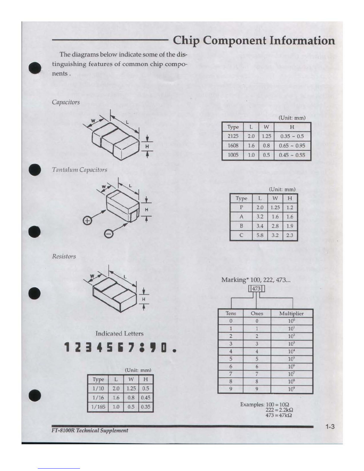
Yaesu FT-8100R Manual

•
•
•
•
YAESU
FT-8100R
Technical
Supplement
•
2
~,
~
· "11"000
~
r2
70
~
--
--
.--
---
--
~
r
tr
"
'I'
,
!
'!(
'
!1
"
!
'!
1
"1
~
VERTEX STANDARD CO., LTD.
4"",-8 NakamegufQ. Meguro-Ku.Toltyo 15:l-8644. Japan
VERTEX STANDARD
usHead
qua
rters
17210 Edwards Rd..
~ff
~O'
.
CA 90703. U,S,A,
Inte
ma
lional
Div
isio
n
8350 NW , 52nd Terrace. Sufle 201, Miami, FL 33166,
US
.A
YAESU EUROPE B.V.
P.O. Box 75525. 1118 ZN Schlphol, The Nelhe
r1
i1nds
YAESU UK LTD.
UM
12. Sun Valley Busmess Pari!,. W,nn
a!1
ccee
Winchester. Hampshire.
S023
OlB ,
UK.
YAESU GERMANYGmbH
Am Kronberge' Hang 2.
0-6582
4Schwalbach,GofTn.ny
VERTEX STANDARD HK LTD.
UM
5, ZOIF.. Seaview Centre . 139-141 H()IBun Road.
Kwun Tong. Kowloon . Hong Kong

Contents
General Information and Alignment 1
Intro
du
ction 1
-1
Specifications 1-2
Chip Component Information 1-3
Transceiver Disassembly and PCBAccess 2-1
Lithium B
att
ery Replacem
ent
2-3
Pilot La
mp
Replacem
ent
2-4
Resetting the CPU 2-5
Exploded View &Miscellaneous Parts 2-7
Alignment 2-9
Servicing 3
Circuit Description 3-1
Block Dia
gr
am 3-7
Interconnection Diagram 3-8
Board
Units
(Circuit Diagram, Parts
La
yout,
Part
s
li
st)
.4
144-VCO Unit 4A-I
430-V
CO
Unit 4B
-1
VR-L Unit 4C-I
VR-R Unit 4D-I
144-Main Unit 4E-I
430-Main Unit 4F-I
Panel Unit 4G-I
CONNEC
T-I, -2 Unit 4H-I
Optional Board Unit (Circuit Diagram, Parts
layout
, Parts
Li
st>
5
FTS-22 Tone Squelch Unit 5A-l
MH-36
B6)
DTMF Mi
crophon
e 5B-I
MH-42B
6)
Hand
Scanning Microphone 5C-I
•
•
•
•
•
CU
iout the labelatthe right.and placeit behind the
clear plastic window in the spine of the manual.
~
-
- - - - - - - -
-
- - - - - -
-
IFT-8100R
: Technical
Suppleme
nt
L

•
•
•
-----------------Introduction
•
•
The
m
anual
provid
es the technical
inf
orma-
tion necessary f
or
se
rvicing the
IT-
Bl
OOR
Dual
-
Band mobile
ama
teur transceiver.
Servicing this eq
uip
ment r
equir
es
expe
rtise in
ha
ndlin
gsurface-m
ount
chip components. At-
te
mpts
by n
on
-qu
alified pe
rso
ns to
service
this
equip
me
nt may r
esult
in p
erm
an
ent
dam
age not
covered by the wa rranty, and may be illegal in
some countries.
T
wo
PCB lay
out
dia
gram
s
provid
ed
for each
doub
le-sided
board
in this
tran
sceiver. Each side
of the
board
is referred to by the type of the ma-
j
orit
y of components installed on
that
si
de
(vl
ead
-
IT
-BJooR Tecl,"ic-al Supplement
ed"
or "chip-only" ). In most cases one side has
onl
y chip components, and the other has either
a mi
xtur
e of b
oth
chip and l
ead
ed components
(trim
me
rs, coils, electrolytic capacitors, ICs, etc.),
or le
aded
compone
nts
only.
While we believe the inf
orm
ation in this man -
ual to be correct, Yaesu
Mu
s
en
as
sum
es no lia-
bility f
or
d
ama
ge that may occur as a result of
t
yp
ogr
aph
ical or ot he r er
ro
rs
that
may be
pr
esent. Y
our
coopera
tio
n in p
ointin
g out
any
in
con
sist
en
cies in the te
chni
cal
inf
orm
ation
would be
appr
eciated.
1-1

Specifications
----------------
General
Fre
que
ncy Range:
Cha
nne
l
Step
:
Fre
quency
Stability:
Re
peate
r Shift:
Emission T
ype
:
Anten na
Impedance
:
Supply
Voltage:
Current
Co
nsu
mption:
Operating
T
emp
.Range:
Case Size (WHO):
Weig ht (approx.):
Trans
mitter
RF
Oulput
(H
/M
/U,
Modu
lationType:
Max Deviation:
Spurious Emission:
Distortion (@70%
MOD
.):
Mi
cropho
ne Imped
an
ce:
Neceiver
Circuit Type:
IFs:
12 dB S
INAD
Sensitivity:
Selectivity (-6
/-60
dB),
Image Rejection:
Sque
lch Sensitivity:
Af
Outpu
t:
AF
Outpu
tIm
ped
an
ce:
1-2
(RX) 110 - 550
MH
z, 750 - 1300
MH
z
'"
...
,
ulli/a
, ItIrKUd
(TX) 144 - 148 MHz, 430 - 450
MH
z
5
/10
/
12.5/15
/20/25
/5
0 kHz
±IOppm (-20 °C - +60 °C, VHF)
±5 ppm (_
5°
C - +60 -c,UHF)
±600 kHz (VHF)
±1.
6/5.
0/7.
6 MH z (UHF)
F3 (G3E), F2
(l200bp,
packet), FI (9600bp, packet)
50 Qunbalanced
IX: 13.8 V ±15 %,
Negative
G
rou
nd
Receive: less than 1.0 A
Transmit; 10.0 A
-20 to +60 °C
140 x40 x165 (w
/o
knob)
1.0 kg
50
/20
/5
W(VHF)
30
/20
/5
W(UHF)
Variable reactance
±5 k
Hz
>60 dB
belo
v..· carrier
less tha n 3%
2kQ
Double-
conve
rsion superheter
ody
ne
45.05 MHz
/45
5 kHz (VHF)
58.525
MH
z
/4
55 kHz (UHF)
<0.18
~
V
(MAIN)
<0.25
~
V
(SUB)
12
/2
4 kHz
better than 70 dB
better than O.13IlV
2W@8
Q fo
r5
% THD
4 - 16 Q(8 Qint
erna
l s
pe
aker)
Sprcific
a
t;o
llssu
bjec
t tochd
llge
witho
ll
t Iloticeor obligatioll.
Sp«i/icatiollsguaranteed within
amateur
ba
nds only.
Fr
eqllfrl
cy range
alld
repeater
shift vary
acco
rding to tran
scei
ver
vers
ion,
IT
-Bl
OO
R Technical Supplement
•
•
•
•
•

•Chip Component Information
The diagrams below indicate some of the dis-
tin
gui
shing features of common chip
compo-
nents .
Capac
itors
•
•T
antatusn
Capacitor
s
~~
~-L
~
~
~
if
Resistors
(Uniti mm)
T
yp"
LWH
2125 2.0 1.25 0.35 - 0.5
1608
I.
.0.8 0.65 - 0.95
1005 1.0 0.5 0
.45
-
0.55
(Unit " m m)
Type LWH
P2.0 1.25 1.2
A3.2
I.
. I..
B3.' 2.8 I.,
e5.8 3.2 2.3
•
•
H
T
Indicated
Lett
ers
1 2 3 4 5 , , : , 0 •
(Unit· mm)
Type LWH
1
/10
2.0 1.25 0.5
1/1 6 I.. 0.8 0.45
1/165 1.0 0.5 0.35
IT-8IooR
Tu
hnical Supplement
Marking" 100, 222, 473...
' 73
I I
Tens Ones Multiplier
001
0'
1 1 10'
22 10'
3 3 10'
, , 10'
5 5
1O
~
• • 1
0'
7710'
8810'
9,10'
Examples:
100:
100
222",2.2kQ
473 :47kQ
1-3

Chip
Component
Information
---------
Replacing Chip Components
Chip
components
are
installed. at
the
factory
by a
series
of
robots
.
The
first
one
places a
small
spot
of
adhesive
resin at
the
location
where
each
part
is to be
installed
,
and
later
robots
handle
and
place
parts
using
vacuum
suction.
For single
sided
boar
ds
,solder paste isapplied
and the board is then baked to har
den
the resin
and
flow the
solde
r. For d
ou
ble si
ded
boa
rds,
no
sol
de
r
pa
ste is applied, but the bo
ar
d is
bak
ed
(or
expose
d to ultra-violet light) to cure the re
sin
before dip sol
de
ring.
In our la
bor
at
or
ies
and
service
shops, small
quan
tities of ch
ip
components
are
mou
nted man-
ually
by
applying
a
spot
of resin,placing
with
tweezers
,
and
then soldering by very small
dual
streams of
hot
air
(without
physical contact
dur-
ing
soldering)
. We
remove
parts by first remov-
ing
solder
using
a
vacuum
suction
iron,
which
applies a light
steady
vacuum
at the iron tip,
and
then
breaking
the
adhesive
with tweezers.
The
special
vacuum
/dcsc
ldering
equipme
nt
is rec
omm
end
ed if you expect to
do
a lot of chip
replacem
ent
s. Otherwise, it is
usua
lly possible
to r
emove
and r
epla
ce
chip
components with
on ly a tapered, t
empera
t
ur
e-controll
ed
solder-
ing
iro
n, a set of tweezers and brai
de
d co
ppe
r
sol
de
r wick. Sol
de
ring iron te
mpe
rature should
be be
low
280°C (536
°8
.
1-4
Precautions for Chip Replacement
oDo not disconnect a
chip
forcefully,
or
the
foil
pattern
may
peel off
the
board
.
o
Never
re-usea
chip
component.
Dispose of
all remov
ed
chip
components
immediate-
ly to
avoid
mixing
with
new
parts
.
oLimit soldering time to 3 seconds
or
less to
avoid
dam
aging tileco
mpo
nent and
board
.
Removing Chip Components
oRemove the solder at each joint, one joint at a
time, using so
lde
r wick w
hetted
with nona-
cidic fluxes as s
how
n be
low
.
Avoid
ap
plying
pressure
, and
do
not
attempt
to re
move
tin-
ning
from
the
chip
's electrode.
oG
rasp
the
chip
on
both
sides
with
tweezers
,
and gently twist
the
tweezers
back and fort h
(to br
eak
the
adhesive
bond)
while
alter
nate
-
ly heating each electrod e. Be careful to
avoid
peeling the foil traces f
rom
the boa rd.
Dis
pose
of the chip w
hen
r
em
ov
ed
.
oAfter removing tile chip, use the co
ppe
r braid
and so
lde
ring iron to wick
away
any excess
solder and s
mooth
the
land for installation of
the replacement part.
IT-B
lOOR
T
uhn
icaf SupplemNlt
•
•
•
•
•

•
•
•
•
•
Chip
Component
Information
ln
stalling a Replacement Chip
As the value of so
me
chip com
po
ne
nts
is not
indicated
on
the b
od
y of the chip, be careful to
ge
t the ri
ght
part
for replac
em
ent.
o
App
ly a sma ll
am
oun
t of sol
de
r to
the
land
on one si
de
where the chip is to be installed.
Avo
id too
mu
ch
so
lde
r,
wh
ich may ca
use
br
idging (shorting to other
part
s).
o
Hold
the chip with tweezers in
the
de
sired
position, and apply the sol
de
ring iron
with
a
motion line as
ind
icated by the ar
row
in the
dia
gr
am below. Do not
ap
ply heat for
mor
e
than 3 seconds.
oR
em
ove the twe
eze
rs
and
solder the elec trode
on the other side in
the
m
anner
just described.
IT
-Bl
OOR
Technical Sllppfemellt1-5

Transceiver
Disassembly
&PCB Access
•
•
•
•
•
144M-Main Unit Access
oRemove 2 sc
rews
from each side
of
the
top
and
bottom
cover
and
2 from the
top
(Fig-
ure
1),
•
•
Figure 1
oTilt the re
ar
of
the
top
cove
r
up
w
ar
d. un-
plug
the s
pea
ker wire connector from J
IDO
l
on
the 144M-Main U
nit
, then sli
de
it
out
from the chassis (Do not use force to remove
the
top
cover).This exposes the co
mpo
nent
side of the 144M-Main Unit (Figure 2).
Figure 2
IT-BlOOR Technical Supplement
430M-Main Un
it
Ac
cess
oPlace the
set
u
pside-
dow
n, and r
em
ove 2
screws fr
om
each s
ide
of the
botto
mcover
and 2 from the top (Figure 3).
•
•
Fi
gur
e 3
oTilt the rear of the
bottom
cover
upw
ar
d,
then sli
de
it out from the chassis, to
expose
the co
mpo
nent si
de
of the 430M-Main Unit.
2-1

Transceiver
Disassembly
&PCB Access
Panel Unit Access
oAft
er
r
em
ovin
g the fr
ont
p
an
el fr
om
the •
tr
an
sceiv
er
. r
em
ove 2sc
rews
from r
ear
side
of the front panel (Figure 5).
Connect Unit Access
oAfter
rem
oving the top and bottom
covers
,
to
rem
ove the fr
ont
panel by slightly pry-
ing o
pe
n the latch on the si
de
of the
tran
s-
ceiver. Next, sli
de
the panel out wa rd and
away
f
rom
the transceiver.
oR
em
ove 2 s
crews
fr
om
bo
th the t
op
and
bottom of the front sub panel. And r
em
ove
ascrew from f
ron
t
sub
panel (Figure 4).
•
Figure 4
oPull the f
ront
sub panel to slightly fr
om
the
transceiver, and unplug the connector from
J101
0 0n the 144M-Main Unit, to ex
pose
the
144M-Main Unit.
2-2
Clips
Figure 5
o
Care
fully sepa
rate
the re
ar
case from the
fron t pa nel
(i
tclips at 6
poi
nts at
bot
h the
top
and
bott
om
edges)
. Disc
onn
ect the flat
ribbon
c
ab
le
from
J300t on the DISP Unit
to
expose
the DlSP Unit (Figure 6).
Figure 6
IT-
SIOOR
T
uhnicRl
Supplement
•
•
•
•

Li
thium
Battery
Replacement
J10
05
2-3
unsolder
remove
removeremove J1004
Lithium B
att
ery Replace
DRemove the top cover. Locate Lithium Bat-
tery BTl 001 (P
IN
Q9000696)
on
th
e 144M-
Mai
n Unit .
Note
the polarity and correct
mo
un
ti
ng
of the cell t
ermi
nals.
oUnpl
ug
the wire co
nnec
tor
from J1004,
Jl 005 on the 144M-M
ain
Unit.
oRemove the 9
screws
from 144M-Main Unit.
No
te the location of the 9 screws, as
ind
i-
cate
below.
oU
nso
l
de
r the 3
stud
s from 144M-Main Unit.
Note
the location of the 3 s
tuds
, as indicate
below.
o
Unso
l
de
r the
battery
terminals and r
em
ove
the old cell.
N
ote
:
Do
notdi
spo
seof
the
old
batt
eryin
fire
,
ande"su
re
small child
re
n
ca
nnotplaywith,or
possiblyil/s est the cell.
oM
ou
nt
t
he
replacement cell in the simila r
manner, observing proper polarity when
installi
ng
it.
unsol
de
r
~IGQ
[?
-
IbJ
flI
!
r-,
..
II
..:
I
unso
lde r I~[1j'
'V''"
t -
tl
~
f~\l~~-
~
;
il
A
;:
'-::!~
-05+t
" , "'
S""""
tIi 0
~
~1f"I!l"""
~
e;
""
IQl
.c
!@ ~
I~
IC5'
!II
.
~
'i!i"""
I
"
!lilt
BT1001
r-
\j
~r~
i£l'F;
n';;"'-
11-
.
~.
-.l'l
...
,
:cD
,.]
~~;"
!l&
r
'''~
J
.•
;J:
liO
I:
;&J
D
II
~~~
"
~
~
~
~
~
I'U
1
~
·
~
w
:-w
-
t-
~
~
-
-
~~
,---
--
--,
JI(
1'":.
f:..
=
JiJ'fft&
.•
"'A
&
IBm
..
~15f1l
,@
~
-
I,
.,
,,, <0>
ill
ill -
Gt::r
T=_
..
.
~ ~
;;.,J.
w.....w_ . - P
II!
I!
. .
"'
l~'
5"_
~
•
• i mlllU
~,
'"
i'l
'A~
,p
;Or.:-
"'"
_U •
re
•
!, 1
_,
rL
CJ
-
Zi
,:1/':»
,
.""
( _ '\l
IT-
BlOOR
Technical Supplem,,"t
•
•
•
•
•

Pilot Lamp Replacement
P
ilot
Lamp
Replaceme
nt
o
Remove
and
separate
the
front
panel as
previou
sly described. Note
the
location of
the
4
lamps
, as indicated below.•
•
oTo re
move
it
failed l
am
p, use a low
watt
-
age
soldering iron and forceps to u
nso
lder
and free each lead, then gent ly lift
the
bulb
ou
t of the hole.
oInstall replace
me
nt
bul
bs in
the
reverse
man
ner, t
hen
reass
em
ble the t
ransceiver
case.
2-4
IT
-B
lOOR
Technical Supp lement
•
•
•

•
•
•
•
•
Resetting the CPU
Res etting the CPU
de
ars all mem
or
ies, r
epe
at-
er shifts and other setti
ng
to th
eir
d
efault
s, and
leaves the transceiver CPU in the same state as
when
it
left the factory.
Asoft reset can be done by h
olding
the D
/MR
and REV keys while
sw
itchi
ng
the
tran
sceiver
on. If a Cl'Ij-related problem remains after the
soft reset, a hardreset can be d
on
e as f
ollows
:
oTum the transceiveroft and di
sconn
ect all
cables.
oRemove the top cover.
oT
emp
or
arily short "cross capacitor C1470.
Note
the location of the C1470, as
indi
cat-
ed
below.
C1470 ---+--'.;1
.~
..
~
aimmnIi
,
IT
-SIOOR
Technical SlIpplemfflt
Resetting
the
CPU
o
•
2-5

REF YAESU PiN
D.
"
,,
~
~
""
,U20306001 BINDING HEAD SCREW M
3-
&•
2U2J106001 TAPTITE SCREW M
2'
62
3U07
430I01
PAN HEAD SCREW M2 6'
J8lI
t2
(
4-'
U24205001 TAPTITE SCREW M2
6"
521
SU1
4206001
TAPTITE SCREW M2
6-
6B •
6UJ12001001 OVAL HEAD SCREW 1,126- 48 "
'1
l/3ooI
206001 TAPTITE SCREW
1,1I
2
6-
6•
,
04
3112001 TAPTITE SCREW M2- 129 I
9
04
3116007 TAPTITE SCREW M
Z·
16B I
"
U99OOO"
TAPTITE SCREW M2
-68
•
""
090101
SPEAKER
t9:106433
T92064J8A (Lol
5-
1_
WIRE
ASS'Y
'
''-
Ma
,n~
R352271Q
KNOB (ENG)
RAOOO7200
FRONT
PANEL ASS"Y
R3154210
KNOB (SO
ll
f2pcs)
R
R
R
3!l2
272Q
KNOetAl
CONNEC
T·]
UM
/
R3154
20M
~
tf'
KNOB
fAF
)
{2
pca
)_
~
.
•
R6054387B
SP
ECIAL
NUT (3(lCIl
IT-BJooR
T~ch"i(lrl
Supplt'mnrt
•

l-
- - - - - - - Exploded
View
&
Miscellaneous
Parts
CS15 14001
TOP CASE ASS'y
000
<NEL
I
EL
M2090017
FAN
R3520800
FAN COVER
R7150880
EMRON
430-Ma'"
Un~
CS1515O(J1
BonOM
CASEASS'V
19206228
WIRE
ASS'Y
19206516
WIRE ASS'V (OST USA)
19206225
WIRE ASS'V JOST EXP. AUS)
Non-designated parts are available
only as part of designated assembly.
2-7

-----------------Alignment
•
•
•
•
•
The
Ff
·8100R is carefully aligned at the facto-
ry f
or
the specifi
ed
perf
ormance ac
ross
the
ama
-
t
eu
r b
and
s. Re
alignm
ent
should th
er
efore not be
necessary except in the
eve
nt of a component fail-
ur
e. All compone nt r
epla
c
ement
and
ser
vice
should be
perf
ormed
only by an aut
ho
rized Yae-
su r
epr
esentative, or the w
ar
ranty policymay be
voided.
The
following
proced
u
res
c
ove
r
the
so
me
-
tim es critica l and t
edi
ou s adj
ust
ments that are
not
n
ormall
y
requir
ed
once the
tran
sceiver has
left the fact
or
y.
Ho
wever, if d
amage
occ
urs
and
so
me
parts su
bseq
ue
ntly be replaced,reali
gn-
ment may be required.
If
a sud
de
n
pr
oblem oc-
c
urs
dur
ing n
ormal
ope
ration, it is likely
du
e to
com
po
nent fai
lur
e; reali
gnm
ent
should not be
done until after the faulty co
mpo
nent has been
replac
ed
.
We rec
omm
end
that servicing be
perform
ed
only
by
au
thoriz
ed
Yaes
u
ser
vice
te
chni
ci
an
s
who
are
ex
pe
rienced with t
he
circuit ry and fully
equi
ppe
df
or
r
ep
air and alig
nm
en t. Ther
ef
or
e,
if
a fault is suspected,
con
tact t
he
deal
er
f
rom
w
ho
m t
he
tra nscei
ver
\
v,
15 pu
rr
-ch
ase
d for in-
stru
ctions
reg
ardi
ng r
ep
air. Aut ho
rize
d Yaesu
serv ice technicians reali
gn
all circuits and make
complete
perf
orm
an
ce checks to
ensur
e compli-
ance with specifications after replacing any faulty
com
po
nents.
Tho
se who do
un
dertake
an
y of the follo
win
g
alignments arc cautioned to
pr
oc
eed
at their
ow
n
risk. Probl
em
s caused by unauth
or
ized attempts
at r
ealignm
ent
are n
ot
covered by the warranty
poli
cy. Also, Y
acsu
mu
st res
er
ve the ri
ght
to
change circuits
and
ali
gnm
ent pr
ocedure
s in the
interest of
impro
ved
perf
orman
ce,
without
n
oti
-
f
yin
g o
wn
ers
.
Un
de
r no circu
ms
tances should
an
y
alignm
ent
IT·
BlooR Technical Supplement
be
att
empt
ed
unl
ess
the
n
ormal
fun
cti
on
and
op
er
ati
on
of the tr
an
sceiv
er
are cle
arl
y
und
er
-
stood, th e ca
use
of the ma
lfun
cti
on
has b
een
cle
arly
pinpointed
and
an
y f
ault
y compo
ne
nts
r
epla
c
ed
,
and
t
he
ne
ed
f
or
r
eali
gnm
ent
det
er
-
min
ed
to be
ab
solut
ely nec
es
sar
y.
The foll
owin
g test equip
me
nt (
an
d th
orou
gh
famili
arit
y with its cor
rec
t use) is necessary f
or
comp
lete
re
alignm
ent. C
or
rec
tion of p
ro
ble
ms
ca
use
d by mis
ali
gnm
ent
re
sultin
g
from
use of
improper
test
eq
uip
me
nt is
not
cove
red
under
the
wa
rranty
poli
cy.
Whil
e m ost ste
ps
do not
requir
e all of the equip
me
nt list
ed
, the inte
rac
-
ti
on
s of so
me
ad j
ust
me
nts
may
requir
e that m
or
e
co
mp
lex
ad
ju
stm
ent
s be p
erform
ed
afte
rwa
r
ds.
Do not at
te
m
pt
to
pe
rfo
rm only a si
ng
le st
ep
unless it is clea
rly
is
olat
ed
e
lect
rically
from
all
other steps. Rath
er
, have all t
est
equip
me
nt re
ad
y
bef
or
e
beg
inni
ng
,
and
foll
ow
all of the
ste
ps in a
sect
ion
in the or
de
r p
res
ent
ed
.
Required Test Equipment
oRF Sig
nal
Gener
ator
with
calib
ra
ted
ou
tp
ut
level at 500 MH z
oDeviation Met
er
(Linear Dete
ctor
)
oAC Voltmet
er
oSINAD
Met
er
o
lnline
Wattm
et
er
w ith 5%
acc
u
racy
at
500
MH
z
oRe
gulated
DC Po
wer
Supply
adj
usta
ble
from
lO'
o1
7V
,l
S A
o
5Q..
Q
Dumm
y Load: 100 W
att
s at 500
MH
z
oFre
qu
ency
Co
unter: 100 Hz re
soluti
on
and ±
0.2
ppm
ac
cur
acy at 500
MH
z
O AF Signal Ge
ne
rator
D
OC
Volt
me
ter: hi
gh
imped
an
ce
oUHF Sampling Co upler
2-9

•
•
•
•
•
''''''''
TCU02
NO
h':Signal
level
s
;/1
dB n
it'Tred
toin thealignmcnt
procedure
are
based
on0dBp =05 dBpV.
time f
or
eq ualiza tio n w ith the e
nvi
ron
me
nt
be-
f
ore
alignment.
Wh
en
ev
er
p
ossibl
e, a
lig
n
me
nts s
ho
uld be
mad e
with
osc
illato r shiel
ds
and circ
ui
t
board
s
firmly affixed in place. Also, the test
eq
uip
me
nt
mu
st be th
or
ou
ghl
y
warm
ed
up
be
fore
begin
-
mn
g.
Most
alignm
ent
pr
ocedur
es call f
or
tunin
g
the
trans
ceiver
to the
high
or 10w
band
ed
ge
,
or
to
band
center.
The
a
ctual
frequen
cy
diff
ers
be-
twe
en
different versions,so the technician
should
make s
ur
e of the
band
limits of each
set
to
be
aligned before be
ginn
ing.
UHF
Pll
&
Transmitter
Alignment
Po
ints
VHF Pl l & Tra
nsmi
ner Ali
gnment
Points
VR1002
VR1006
VR1005
VR1001
Alignment
--------------
--
Alignment Preparation &Precautions
A
so-o
dum
my
load
a
nd
inli ne
wa
tt
mete
r
must
be co
nnected
to the a
nten
na jack
in
all pro-
ced
u
res
that call for tr
an
sm
ission, except where
specified othe
rw
ise
.
Co
rrect
alig
n
me
nt is not
possible with
an
antenna.
After completing 0
0('
step.
wad
the foll
owing
step to det
ermine
whether the sa me t
est
equip-
men t will be r
equir
ed .
If
not
, r
em
ove the test
equipment (except power supply,
dumm
y load
and wa ttmeter,
if
connected) before proceeding.
Cor
rect align
me
nt re
qu
ires that th e ambient
tem
pera
t
ure
be the sa
me
.15 t
hat
of the
tr
an
sceiv-
cr
and test equipment, and
tha
t this
tem
per
atur
e
t'ot.
'
held
co
nstant
betwee
n 20
and
30 °C (68 - 86
"F).
If
the
tr
an
sceiv
er
is
broug
ht i
nto
the sh
op
from
hot
or
co
ld
air
it
s
hou
ld be allowed some
2-10
rT
..slOOR
T
uhn
iclII Sllpplement

Alignment
PLL &Transmitter Transmitters
•Set
up
the test
equipment
as
shown
for trans-VHF
Power
Output
nutter alignment. Maintain the
supply
voltage oCouple the frequency counter to sample the
at I3.8V IX: for all steps. RFoutput.
I
Regul
;l1~
~
S~mp
"
ng
1" lIne
-~
Io
Tune
to
band
center (for
the
version
being
138VPSU
'""
..
'
wanmel,",
DummyLoad aligned),
and
press the
lOW
button if neces-
~
F'eq
CouM.f I
sary
, to select low
power
output.
L-
.-i
Dev1~toon
Mt'!e<IoKey
the
transmitter
and
adju
st TC1001 on
the
I144-Main Unit to
mat
ch the
display
to the
Lf
'"
G<~
,".
counter frequency (
within
100 Hz).
~
I\C von me1er I
AI;
VoIlm01tet Io
Tune
to
band
center (f
or
the
version
being
•aligned),
and
pre
ss the LOW
button
,if neces-
Transmitte
r
Alignment
Setup
sary
, to select high
power
output.
oKey
the
tran
smitter
and
adjust VR1001 on
the
PLL VCV (Varactor Cont
ro
i Voltage) 144-Main Unit for 50
watts
on the
wattmeter
.
VHF Band o
Press
the
lOW
button
to select
MID
powe
r,
oConnect
Voltmeter
between
VCV
test
point
key
the
transmitter,
and
confirm 15 to 25
watts
on the 144-Main Unit and chassis
ground
.on
the
wattmeter.
•oRefer to
the
chart below,
transmit
and
adjust
oPress
the
lOW
button
to select
lOW
power
,
TC4302 on
the
144-VCO Unit for
the
indi
cat- key
the
transmitter
and
adjust VR1002 on
the
ed
volta
ge
at
that
li
sted
frequency
.
Adjust
144-Main Unit for 4 to 6
watt
s
on
the
wattme-
TC4301 as necessary for
the
required voltage ter.
while receiving. VHF
Tran
smitter
Deviatio
n
R"
4<
T" VCV A
lignmmt
Dala oWhile
tuned
to
the
center of
the
band
,adjust
•Main Band Sub
Band
the AF
generator
attenuator
for 50
mVoutput
FK'\j
uency Voltag... Frequency Voltage at 1
kHz
to
the
MIC jack.
R, T, R, T, R,
r.
""
T, oKey
the
transmitter
and
adjust VR1006 on
the
I.... I.... 35V 2.0V HO .2
5V
.144-Main Unit for
±45
kHz
IV
ers
. USA ±4.0
H" HIJ
aov
4,OV 1% .JO V .kHz)
deviation
on
the
deviation
meter
.
UHF
Ban
do
Redu
ce
the
AF inje
ction
until
the d e
viation
o
Connect
Voltmeter
between
VCV
test
point
meter
sho
ws ±3.0 kHz (Vers. USA: ±2.7 kHz)
on
the
430-Main Unit
and
chassis g
round
.deviation, and confirm that
the
injection level
o
Tun
e to
the
required
channel,
t
ransmit
and
is 55 mV.
adjust
TC4402
on
the
430-VCO Unit for the
vo
ltage
indicated in
the
table.
•oWhile receiving,adjust TC4401 for
the
corre-
sponding
voltage
for that f
requen
cy.
2-11
IT-B
lOOR
Technical Supplement

Alignment
----------------
UHF Power Output
o
Co
uple the frequency co
unte
r to
sampl
e the
RF output.
o
Tun
e to
band
center (for the version being
align
ed
), and press the
LOW
butto
nif neces-
sary
, to select low power output.
oKey the tr
an
smitt
er
and adjust TC2002 on the
430-M
ain
Unit to match the d isplay to the
cou
nter fr
equen
cy (within 100 Hz).
oTu ne to ba nd center (for the version
bein
g
alig
ned
), and
pr
ess the
LOW
butto
n , if ncc es-
sary, to select high
powe
r output.
oKey the transmitter and a
dju
st VR2004on the
430-M
ain
Unit for 35
watts
on the watt
mete
r.
o
Pr
ess the
LOW
bu
tton to select MID power,
key the transmitt
er
, and confirm 15 to 25watts
on the wattmeter.
oPress the
LOW
butt
on to select LOW power,
key the t
ran
sm
itt
er
and adjust VR2005 on the
430-Main Unit for 4 to 6 watts on the wattme-
ter.
UHFTransnuttcr
Deviation
oWhile tuned to the ce
nte
r of the band, adjust
the AF gener
ato
ratte
nuator
for 50 mVout
put
at 1 kHz to the MIC jack.
oKey the transmitter and
ad
just
VR1005
on the
144-M
ain
Unit for ±4.5 kHz (Vers. USA ±4.0
kHz) deviati
on
on the deviati
on
meter.
oRed uce the AF injection un til the deviati
on
mete
r s
hows
±3.0 kHz IVers. USA: ±2.7 kHz)
deviatio
n, and confirm that till' injec
tion
level
is 5.5 mV.
2-12
Receivers
Set
up
the test equipment as sh
ow
n h
er
e for
receiv
er
alignment.
Reg ulalecl
13 8'-'PSU
RF
Sill
....i
GeneralOt
Receiver
Alignment
Setup
VHF Inferstage Transformers
oConnect Voltmeter be
twee
nS
mater
test point
on the 144-Main Unit and chassis
gro
und.
o
Tun
e the tr
an
sceiv
er
and
RF signa l gene
rato
r
to the center of the VHF b
and
. M
od
ulate the
RF signal ge
ner
ator
with ±3.5 k
Hz
dev
iation
of a 1 kHz t
on
e.
DAdjust 11
003
and T1
005
- T1
008
on
the 144-
Main Unit for max
imum
volt
age
on the volt-
met
er
.
oConfirm -8 dB
,",
or better 12 dB S
INAD
at the
high and low band
edges
.
UHF Illterstage Transformers
oConnect voltmeter between
Sm
eter test
poin
t
on the 43O-Main Unit and chassis
gro
und.
o
Tun
e the
tran
scei
ver
and RF signa l
gene
rator
to
the
ce
nte
r of the U
HF
band .
Modul
ate the
RF signal
generat
or with ±3.5 k
Hz
devia ti
on
of a 1 kHz
tone
.
DAdjust
T2004
on
the 430-Main Unit for maxi-
mum
voltage on the voltmeter.
oConfirm -8 dB
,",
or better 12 dB SINA D at the
high and low
ban
dedges.
IT
-8looR Techniclll Supplement
•
•
•
•
•

----------------Alignment
•
•
VHF Squelch Preset
oTune to the ce
nte
r of the VHF b
and
.With no
signal at the a
nte
nna jack.
oSet the
SQl
contro
l to the 10-0' clock posi-
tion,
and
adjust VR1003 0n the 144
·M
ain Unit
so the squelch just closes.
UHF
Squelch
Preset
oTune to the center of the U
HF
band. With no
signal at the antenna jack.
oSet the
SQl
control to
the
10·0' clock
po
si-
tion, a
nd
ad just VR
2002
so the squelch j
ust
closes.
VHF S-Meter Calibration
oAt the cen
ter
of
the VHF band, inject 25 dBfl
RF
mod
ulat
ed
wit
h ±3.5 kHz deviati
on
of
a 1
kHz tone to the ante
nna
connector. Adj
ust
VR1004
on the 144-Main Unit so
th
at all S-
meter segments are j
ust
on.
UHFS-Meter
Ca
librat
ion
oTune the transceiver and RF signal
ge
nera
tor
to the center
of
the UHF
ban
d and with the
sa
me
injection level a
nd
mod
u
lation
,
adjust
VR2003 so t
hat
all
5-me
ter
segmen
ts
are
just
on.
•
•
•
VHF Receiver Alignment Points
UHF Receiver Alignment Points
VR2002
S-meter
T
..
tP
olnl
2-13

•
•
•
•
•
The
Fr
-Sl 00R circuitry consists
of
three
ma-
jor
board
s: the 144
and
430-Main Units,
the
Pan-
el Unit
and
numerous
min
or
board
s
that
mount
on these. The
Main
Unit
includes
the
receiv
er
front en
ds
, IF
and
Pl
l subsystem ICs,
and
sup-
p
ort
s
daughter
bo
ards
for
transmit
st
ages
, local
ve
Os
,
suppl
y re
gulati
on
and
swit
ching circuits,
the mi
cr
opro
cessors,
and
tone
ge
nerator
/
decod
-
cr
chips. Whilt.' re
ading
this description,
you
C.
lO
refer to the
blo
ck
diagram
for an
overview
of the
major circuit blocks,
and
to
the
schematic d ia-
grams f
or
component details.
All tem.tI Duplexer
In
com
ing RF
from
the antenna jack p .1S
Sl
'S
throu
gh a high-pass and I
OW
-P.1
SS filter n
etwork
on
the "30-M
ain
Unit before application to two
band-switching n
et
w
orks
: coil L2031,
diodes
02
005, 0 2014
,0203
0 and capacitors C2 146,
C2 l47, C2148, C2152, and
resistor
R2115 on
the
"
30-1\.1
ain
Unit for UHF signals;
and
coil Ll 025,
di
odes
01
012, 0101 9,
and
01064
on
the 144-Main
Unit,
and
capacitors C l l..7, C I148, C1120, resis-
tor RI106 on till.' I....-Main Unit for VHF signals.
These
networks
filter VHF signals from the UHF
receiver and UHF signals from
the
VHF receiv-
er
, allowing each band to
operate
independent-
ly
wh
ile
shari
ng the
same
ante
nna connection.
VHF Rece
pt
ion
VHF
signals
pas
sed
by
the
duplexer
are
ap-
plied to a
vara
ctor
-tuned
band-pass
filter con-
sisting of
Tt
OO6
,Tl
OO7
,01 008
and
01
009, aft
er
RF amplification by
Ql
OO2
(S GM2016M). The
amplified
RF is
passed
through
another
RF
am-
plifier
Ql
OOI
(3SK131-V12),
then
band
-pass fil-
t
ered
again
by varact
or-tuned
resonators
TlDOS
,
TI
OO
8,
Dl
OIO, and DI
Oll
,th
en
fed
through
di-
ode
swit
ch
01
003 (MA80WK) to
the
FET Bal-
an
ced
Mixer
TI002
/TI003
and
Q1100
/Qll01
IT
-B
lOOR
Tl'chn
ictll
Suppll'
mm
t
Circuit
Description
(2SK302GR).
Buffered 155.05 - 219.05
MHz
output
from
the
144-VCO Unit is amplified by QlOO7(2SC3120)
and
applied to
the
Ist mixer. The resulting 45.05-
MHz
1st mixer
product
i...passed
through
mono-
lithic crystal filters
XFtOOt
and
XFl002 to
strip
away
all
but
the
de
sired
signal
,
which
is
then
amplified by QlOO3(2SC2714Y)beforedelivery
to FM IF
subsy
stem
Ie
Ql009
(TK10930V), con-
taining the 2nd mixer, 2nd local oscillator, limit-
er a
mp
lifier, noise a
mp
lifier, Scmeter a
mp
lifier
and squelch gates. A 2nd local signal is generat-
ed
from 45.505 MH z crystal XlOOl,
whi
ch
pro-
du
ces the 455
kl
lz 2nd IF
when
mixed
with
the
1st IF
signal
within
QI
OO9
. The
2nd
IF is
passed
throu
gh ceramic filt
er
C
FlOO
l to
strip
awa
y un-
wanted
mixer
produ
cts,
and
is
then
applied
to
the limiter amp in QI
OO9
,
wh
ich r
emov
es
ampli
-
tude
variations in the " 55 kHz IF
bef
ore
det
ec-
ti
on
of
the
speec h by ceramic
dis
criminator
C
DlOO
I.
VHF Squelch
CO
lltrol
When
no carrier is re
ceived
,noise at
the
out-
put
of
the
dete
ctor
stage
in Q
l009
is
amplified
and
b
an
d-pass filtered by the noise a
mp
section
of
Ql009
and the netw
or
k be
twee
n pin 19 and
20,
and
then
rectified by 0 1014.
The
resu
lting
IX:
squelch control voltage is passed to
pin
79 of
CPU
Qll04
.While no carrier is received,
pin
8
on
QII04
remains "Lo
w,"
signaling
pin
8 of CPU
QIHH
(M3
17
02E4l
which
prodo
ces
the
BUSY
indication
on the
displa
y
wh
en
the
squelch
is
o
pe
n.
VHF AF Output
Detected
audi
ofrom
pin
12 of
Ql
009
passes
through
the d
e-empha
sis
network
consisting of
RIMS
and
CI078, and
high
-pass filter consisting
of Q1114-3 (NJ M2902M)
and
associated circuit-
3-1
Other manuals for FT-8100R
4
Table of contents
Other Yaesu Transceiver manuals

Yaesu
Yaesu FTDX5000 CAT BOOK Service manual

Yaesu
Yaesu FTM-300DR User manual

Yaesu
Yaesu FT-8900R User manual

Yaesu
Yaesu VX-8R User manual

Yaesu
Yaesu FT-301 User manual

Yaesu
Yaesu FT-757GX II Owner's manual

Yaesu
Yaesu FT-227R Memorizer User manual

Yaesu
Yaesu FT-4700RH User manual

Yaesu
Yaesu FT-101ZD User manual

Yaesu
Yaesu FTdx3000 Series Product guide