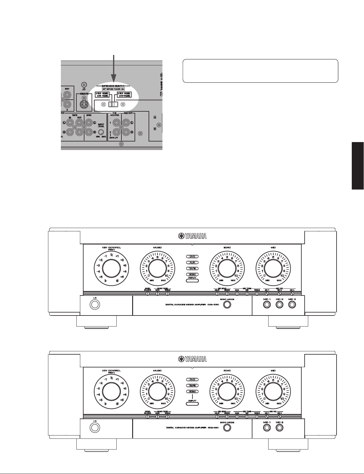
Yamaha KMA-1080 User manual

This manual has been provided for the use of authorized YAMAHA Retailers and their service personnel.
It has been assumed that basic service procedures inherent to the industry, and more specifically YAMAHA Products, are already
known and understood by the users, and have therefore not been restated.
WARNING: Failure to follow appropriate service and safety procedures when servicing this product may result in personal
injury, destruction of expensive components, and failure of the product to perform as specified. For these reasons,
we advise all YAMAHA product owners that any service required should be performed by an authorized YAMA-
HA Retailer or the appointed service representative.
IMPORTANT: The presentation or sale of this manual to any individual or firm does not constitute authorization, certification or
recognition of any applicable technical capabilities, or establish a principle-agent relationship of any form.
The data provided is believed to be accurate and applicable to the unit(s) indicated on the cover. The research, engineering, and
service departments of YAMAHA are continually striving to improve YAMAHA products. Modifications are, therefore, inevitable
and specifications are subject to change without notice or obligation to retrofit. Should any discrepancy appear to exist, please contact
the distributor's Service Division.
WARNING: Static discharges can destroy expensive components. Discharge any static electricity your body may have accumu-
lated by grounding yourself to the ground buss in the unit (heavy gauge black wires connect to this buss).
IMPORTANT: Turn the unit OFF during disassembly and part replacement. Recheck all work before you apply power to the unit.
IMPORTANT NOTICE
101164
SERVICE MANUAL
CONFIRMATION OF IDLING CURRENT OF AMP
UNIT ............................................................................ 14
IC DATA ................................................................ 15–17
BLOCK DIAGRAM..................................................... 18
PIN CONNECTION DIAGRAMS ................................ 19
PRINTED CIRCUIT BOARDS .............................. 20–30
SCHEMATIC DIAGRAMS ..................................... 31–37
REPLACEMENT PARTS LIST ............................. 39–47
REMOTE CONTROL .................................................. 48
SETUP MODE ...................................................... 49–51
CONTENTS
■
TO SERVICE PERSONNEL ......................................... 2
IMPEDANCE SELECTOR ............................................ 3
FRONT PANELS .......................................................... 3
REAR PANELS ............................................................. 4
REMOTE CONTROL PANEL ....................................... 5
SPECIFICATIONS .................................................... 5–6
INTERNAL VIEW .......................................................... 6
DISASSEMBLY PROCEDURES .................................. 7
INDICATION OF PROTECTION INFORMATION ........ 8
SELF-DIAGNOSTIC FUNCTION ............................ 9–13
Copyright © 2010 YAMAHA CORPORATION. All rights reserved.
This manual is copyrighted by YAMAHA and may not be copied or
redistributed either in print or electronically without permission.
’10.02
DIGITAL KARAOKE MIXING AMPLIFIER
KMA-1080/KMA-980
For T model
KMA-1080/KMA-980

2
KMA-1080/KMA-980
KMA-1080/KMA-980
TO SERVICE PERSONNEL
■
1. Critical Components Information
Components having special characteristics are marked Z
and must be replaced with parts having specifications equal
to those originally installed.
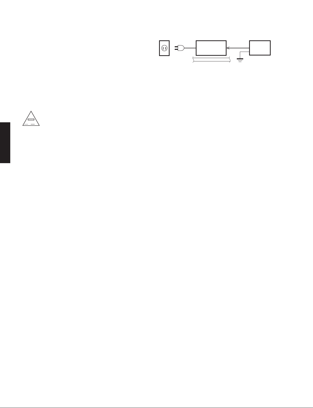
2. Leakage Current Measurement (For 120V Models Only)
When service has been completed, it is imperative to verify
that all exposed conductive surfaces are properly insulated
from supply circuits.
●Meter impedance should be equivalent to 1500 ohms shunt-
ed by 0.15µF.
AC LEAKAGE
TESTER OR
EQUIVALENT
EQUIPMENT
UNDER TEST
INSULATING
TABLE
WALL
OUTLET
WARNING: CHEMICAL CONTENT NOTICE!
This product contains chemicals known to the State of California to cause cancer, or birth defects or other reproductive
harm.
DO NOT PLACE SOLDER, ELECTRICAL/ELECTRONIC OR PLASTIC COMPONENTS IN YOUR MOUTH FOR ANY
REASON WHAT SO EVER!
Avoid prolonged, unprotected contact between solder and your skin! When soldering, do not inhale solder fumes or ex-
pose eyes to solder/flux vapor!
If you come in contact with solder or components located inside the enclosure of this product, wash your hands before
handling food.
●Leakage current must not exceed 0.5mA.
●Be sure to test for leakage with the AC plug in both
polarities.
About Lead Free Solder
All of the P.C.B.s installed in this unit and solder joints are soldered using the lead free solder.
Among some types of lead free solder currently available, it is recommended to use one of the following types for the repair work.
• Sn + Ag + Cu (tin + silver + copper)
• Sn + Cu (tin + copper)
• Sn + Zn + Bi (tin + zinc + bismuth)
Caution:
As the melting point temperature of the lead free solder is about 30°C to 40°C (50°F to 70°F) higher than that of the lead solder, be
sure to use a soldering iron suitable to each solder.
“CAUTION”
“F401: FOR CONTINUED PROTECTION AGAINST RISK OF FIRE, REPLACE ONLY WITH SAME TYPE
2.5A, 250V FUSE.”
“F402: FOR CONTINUED PROTECTION AGAINST RISK OF FIRE, REPLACE ONLY WITH SAME TYPE
4A, 250V (KMA-1080) / 3.15A, 250V (KMA-980) FUSE.”
AV
WARNING: Lithium batteries
CAUTION
Danger of explosion if battery is incorrectly replaced.
Replace only with the same or equivalent type.
WARNING: Lithium batteries are dangerous because
they can be exploded by improper handling. Observe
the following precautions when handling or replacing
lithium batteries.
• Leave lithium battery replacement to qualified service
personnel.
• Always replace with batteries of the same type.
• When installing on the PC board by soldering, solder
using the connection terminals provided on the battery
cells. Never solder directly to the cells. Perform the
soldering as quickly as possible.
• Never reverse the battery polarities when installing.
• Do not short the batteries.
• Do not attempt to recharge these batteries.
• Do not disassemble the batteries.
• Never heat batteries or throw them into fire.
ADVARSEL!
Lithiumbatteri –Eksplosionsfare ved fejlagtig håndtering.
Udskiftning må kun ske med batteri af samme fabrikat
og type. Levér det brugte batteri tilbage til leverandøren.
VARNING
Explosionsfara vid felaktigt batteribyte. Använd samma
batterityp eller an ekvivalent typ som rekommenderas av
apparattillverkaren. Kassera använt batteri enligt fabri-
kantens instruktion.
VAROITUS
Paristo voi räjähtää, jos se on virheellisesti asennettu.
Vaihda paristo ainoastaan laitevalmistajan suosittele-
maan tyyppiin. Hävitä käytetty peristo valmistajan ohje-
iden mukaisesti.

3
KMA-1080/KMA-980
KMA-1080/KMA-980
IMPEDANCE SELECTOR
■
FRONT PANELS
■
▼KMA-1080
▼KMA-980
IMPEDANCE SELECTOR
WARNING:
Do not change IMPEDANCE SELECTOR setting while the power
to this unit is on, otherwise this unit may be damaged.
KMA-1080 model

4
KMA-1080/KMA-980
KMA-1080/KMA-980
REAR PANELS
■
▼KMA-1080
▼KMA-980

5
KMA-1080/KMA-980
KMA-1080/KMA-980
REMOTE CONTROL PANEL
■
SPECIFICATIONS
■
AMPLIFIER SECTION
Minimum RMS Output Power
L/R (1 kHz, 1% THD, 8-ohms)
KMA-1080 160 W + 160 W
KMA-980 120 W + 120 W
Maximum Useful Output Power (JEITA)
L/R (1 kHz, 10% THD, 8-ohms)
KMA-1080 200 W + 200 W
KMA-980 150 W + 150 W
Damping Factor
20 Hz to 20 kHz, 8-ohms 60 or more
Input Sensitivity/Input Impedance
DVD etc. 200 mV/42 k-ohms
MIC 6 mV/20 k-ohms
Maximum Input Voltage
DVD etc. 2.3 V or more
MIC 60 mV or more
Rated Output Voltage/Output Impedance
SUBWOOFER 2.0 V/1.2 k-ohms
REC OUT/PRE OUT 1.0 V/1.2 k-ohms
Total Harmonic Distortion (1 kHz)
DVD etc. to SP OUT
KMA-1080 (80 W/8-ohms) 0.1% or less
KMA-980 (60 W/8-ohms) 0.1% or less
Signal to Noise Rate (IHF-A Network)
DVD etc., Input shorted (200 mV) 85 dB or more
MIC, Input shorted (6 mV) 75 dB or more
Residual Noise (IHF-A Network) 180 µV or less
Channel Separation (1 kHz)
DVD etc., Input 5.1 k-ohms shorted 55 dB or more
Tone Control Characteristics
MUSIC
Bass boost/cut (100 Hz) ± 12 dB
Treble boost/cut (10 kHz) ± 12 dB
MIC
Bass boost/cut (100 Hz) ± 12 dB
Mid boost/cut (1 kHz) ± 12 dB
Treble boost/cut (10 kHz) ± 10 dB
Gain Tracking Error (0 to -60 dB) 2.0 dB or less
GENERAL
Power Supply AC220 V, 50 Hz
Power Consumption
KMA-1080 200 W
KMA-980 145 W
AC Outlet
2 switched outlets 100 W max. total
Dimensions (W x H x D) 435 x 150 x 430 mm
(17-1/8" x 5-7/8" x 16-7/8")
Weight
KMA-1080 11.3 kg (24.9 lbs.)
KMA-980 10.7 kg (23.6 lbs.)
Finish Black color
Accessories Remote control x 1
Lithium battery (CR2025) x 1
* Specifications are subject to change without notice.
T ............ Chinese model

6
KMA-1080/KMA-980
KMA-1080/KMA-980
435 (17-1/8˝)
18 (5/8˝)
132 (5-1/4˝)
150 (5-7/8˝)
376 (14-3/4˝)
430 (16-7/8˝)
40 (1-5/8˝)
14 (1/2˝)
DIMENSIONS
Unit : mm (inch)
INTERNAL VIEW
■
qMAIN (5) P.C.B.
wMAIN (3) P.C.B. (KMA-1080)
MAIN (4) P.C.B. (KMA-980)
eOPERATION (1) P.C.B.
rDSP (2) P.C.B.
tDSP (1) P.C.B.
yMAIN (1) P.C.B.
uMAIN (2) P.C.B.
iFUNCTION (1) P.C.B.
oOPERATION (7) P.C.B.
!0 OPERATION (2) P.C.B.
!1 FUNCTION (2) P.C.B.
!2 OPERATION (5) P.C.B. (KMA-1080)
OPERATION (6) P.C.B. (KMA-980)
!3 OPERATION (4) P.C.B.
Front view
Top view /4 0)1
62 *
-

7
KMA-1080/KMA-980
KMA-1080/KMA-980
DISASSEMBLY PROCEDURES
■
(Remove parts in the order as numbered.)
1. Removal of Top Cover
a. Remove 8 screws (q) and 2 screws (w). (Fig. 1)
b. Slide the top cover rearward to remove it. (Fig. 1)
2. Removal of Front Panel Unit
a. Remove 5 screws (e) and 4 screws (r). (Fig. 1)
b. Remove CB2 (FUNCTION(1) P.C.B.), CB3, CB15
and CB562. (Fig. 1)
c. Remove the front panel unit. (Fig. 1)
Fig. 1
Fig. 2
3. Removal of OPERATION (1) P.C.B.
a. Remove 6 (KMA-1080) / 3 (KMA-980) screws (t)
and 2 nuts (y). (Fig. 2)
b. Remove CB237. (Fig. 2)
c. Remove CB238 and CB411 (KMA-1080). (Fig. 2)
d. Remove the OPERATION (1) P.C.B.. (Fig. 2)
Top cover
:
:@
CB2
(FUNCTION(1) P.C.B.)
CB15
CB562
;
;
.
Front panel unit
CB3
==
==
=BB
CB237 OPERATION (1) P.C.B.
KMA-1080 model
CB238
KMA-1080 model
CB411

8
KMA-1080/KMA-980
KMA-1080/KMA-980
INDICATION OF PROTECTION INFORMATION
■
If any of indicators shown below flashes after turning on the power to this unit, it means that the protection func-
tion is at work and normal operation is not available.
●
Details of Protection Information
a. DC protection
Cause: Abnormal DC voltage of amplifier output L/R
Normal value: 0.312 to 2.327 V
Detection port: PRD (58 pin of microprocessor IC15)
Detected at: Amplifier output L/Rch of MAIN P.C.B.
b. I protection
Cause: Excess current flow into amplifier
Normal value: Low (0 V)
Detection port:
PRI (56 pin of microprocessor IC15)
Detected at: Amplifier output L/Rch of MAIN P.C.B.
c. TH protection
Cause 1: Abnormal temperature of heatsink.
Normal value: 0.3 to 1.5 V
Detection port: TH_R (57 pin of microprocessor IC15)
Detected at: Heatsink temperature detection IC401 of MAIN P.C.B.
Cause 2: Abnormal temperature of power transformer.
Normal value: 0.3 to 1.4 V
Detection port: TH_R2 (54 pin of microprocessor IC15)
Detected at: Power transformer temperature detection IC402 of MAIN P.C.B.
MUSIC indicator flashing: DC protection MIC indicator flashing: TH protection
ECHO indicator flashing: I protection
KEY CONTROL indicator flashing in red/green alternately

9
KMA-1080/KMA-980
KMA-1080/KMA-980
This unit has self-diagnostic functions that are intended for inspection, measurement and location of faulty point.
There are 12 main menu items, each of which has sub-menu items.
Listed in the table below are main menu items and sub-menu items.
SELF-DIAGNOSTIC FUNCTION
■
No.
Main menu Sub-menu
1 FIRMWARE VERSION a Main Microprocessor Firmware Version
b DSP Microprocessor Firmware Version
2 TEMPERATURE of HEATSINK
a Monitor
b Maximum
c Minimum
3 TEMPERATURE of POWER TRANSFORMER
a Monitor
b Maximum
c Minimum
4 DC VOLTAGE a DC Voltage
5 PROTECTION HISTORY
a History 1
b History 2
c History 3
6 CHECKSUM a Upper bit
b Lower bit
7 ANALOG CHECK
a DVD
b AUX (KMA-1080) / TAPE (KMA-980)
c TAPE (KMA-1080) / BGM (KMA-980)
d BGM (KMA-1080) / ‒ (KMA-980)
8 DSP MUSIC CHECK
a DVD
b AUX (KMA-1080) / TAPE (KMA-980)
c TAPE (KMA-1080) / BGM (KMA-980)
d BGM (KMA-1080) / ‒ (KMA-980)
9 DSP MIC CHECK aLch
bRch
10 INDICATOR CHECK
a All Light up
b All Off
c Automatic Sequential Lighting
11 INPUT MODE
a DVD
b AUX (KMA-1080) / TAPE (KMA-980)
c TAPE (KMA-1080) / BGM (KMA-980)
d BGM (KMA-1080) / ‒ (KMA-980)

10
KMA-1080/KMA-980
KMA-1080/KMA-980
●Starting Self-Diagnostic Function
While pressing theINPUT key of this unit, press thePOWER switch to turn ON the power.
“INPUT” key
“POWER” switch
●Canceling Self-Diagnostic Function
Press thePOWER switch of this unit to turn OFF the power.
●Operation Procedure of Main menu and Sub-menu
There are 12 main menu items, each of them having sub-menu items.
Main menu selection
Select the main menu usingKEY CONTROL knob.
Sub-menu selection
Select the sub-menu usingINPUT key.
Mainmenuindicator(litinred) Sub-menuindicator
Main menu No. KEY CONTROL indicators
1
2+1
3+2
4+3
5+4
6+5
7-1
8-2
9-3
10 - 4
11 - 5
Sub-menu Code INPUT indicators
KMA-1080 KMA-980
a DVD DVD
b AUX TAPE
c TAPE BGM
d BGM ‒

11
KMA-1080/KMA-980
KMA-1080/KMA-980
●
Details of Self-Diagnostic Function menu
1. FIRMWARE VERSION
The firmware version is indicated.
a. Main Microprocessor Firmware Version
b. DSP Microprocessor Firmware Version
2. TEMPERATURE of HEATSINK
The temperature of heatsink is indicated.
a. Monitor: Current temperature
b. Maximum: Highest value
c. Minimum: Lowest value
4. DC VOLTAGE
The DC voltage of amplifier output L/R is indicated.
5. PROTECTION HISTORY
The 3 protection histories are indicated.
0. No protection
1. DC protection
2. I protection
3. TH protection
Version: 1.00
+026 ℃
Voltage: 0.00V
History 1 (Latest) History 2 History 3
(+: Off, -: Lit (Amber))
+026 ℃
(+: Off, -: Lit (Amber))
3. TEMPERATURE of POWER TRANSFORMER
The temperature of power transformer is indicated.
a. Monitor: Current temperature
b. Maximum: Highest value
c. Minimum: Lowest value

12
KMA-1080/KMA-980
KMA-1080/KMA-980
6. CHECKSUM
The checksum value is indicated in the decimal number.
a. Upper bit
b. Lower bit
Gm_L
Gm_R
Gv
DSP6
LR
LR
LR
L
DSP
Through SW Music
D-Vol
Music
D-Vol
Music
SW Mic
Mic DRY
A/D
A/D
D/A
D/A
Misic
Mic
ANALOG CHECK
DSP MUSIC CHECK
DSP MIC CHECK
Menu
KEY
CONTROL
Volume INPUT Gm_L Gm_R Gv SW
Music
SW
Mic
MUSIC ECHO MIC
ANALOG CHECK Active
(Min) Min Active
(Min)
Active
(DVD) – ∞– ∞– ∞through –
(on)
DSP MUSIC CHECK – ∞0 dB Active
(Min)
Active
(DVD) – ∞– ∞0 dB –
(through)
–
(on)
DSP MIC CHECK L ch
Active
(Min) Min – ∞off 0 dB – ∞– ∞DSP –
(on)
DSP MIC CHECK R ch
Active
(Min) Min – ∞off – ∞0 dB – ∞DSP –
(on)
Fig. 3
INPUT select L ch: 0 to 4, R ch: 6 to 10
“ECHO MODE” key
Upperbit 054 (decimal number) m36 (Hexadecimal)
Lowerbit 169 (decimal number) mA9 (Hexadecimal)
Checksum value: 36A9
7. ANALOG CHECK
The signal passage is checked. (Fig. 3)
INPUT select: DVD, AUX (KMA-1080 model), TAPE, BGM
MUTE ON/OFF: "ECHO MODE" key (ON: Lit (amber), OFF: Off)
8. DSP MUSIC CHECK
The signal passage is checked. (Fig. 3)
INPUT select: DVD, AUX (KMA-1080 model), TAPE, BGM
9. DSP MIC CHECK
The signal passage is checked. (Fig. 3)
Channel select: "ECHO MODE" key
a. L ch (0 to 4 of MIC indicator light up)
b. R ch (6 to 10 of MIC indicator light up)

13
KMA-1080/KMA-980
KMA-1080/KMA-980
10. INDICATOR CHECK
This menu is used to check the indicators.
a. All Light up
b. All Off
c. Automatic Sequential Lighting
11. INPUT MODE
Both Auto and Manual of INPUT mode are activated.

14
KMA-1080/KMA-980
KMA-1080/KMA-980
CONFIRMATION OF IDLING CURRENT OF AMP UNIT
■
R429 (L ch)
R430(R ch)
TP413–TP415 (L ch)
TP414–TP416 (R ch)
Open (cut off)
20 mV – 350mV
(DC)
R429
R430
TP416
TP414
TP415
TP413
Rear side
Front side
Item Condition Test point Rating Remark
Idling current No input signal
Wait for 2–3 minutes
TP413–TP415 (L ch) DC 20–350mV
If measured voltage exceeds 350 mV,
open (cut off) R429(L ch), R430 (R ch)
and reconfirm the voltage.
Attention
If the measured voltage exceeds
350mV after an amplifier repair, first
check for a defective component be-
fore cutting the bias resistor.
TP414–TP416 (R ch)

15
KMA-1080/KMA-980
Pin No.
Port Name Function Name I/O Detail of Function Default
1 P33/SSI SDATA O For device, commonly used DATA Low
2 P34/SDA/SCS FSTL O LED/key PT6313 / NJM7318 STB High
3 MODE MODE
4 P43/XCIN SSDATA O LED/key PT6313 / NJM7318 DATA Low
5 P44/XCOUT SSCLK O LED/key PT6313 / NJM7318 SCK Low
6 RESET /RESET
7 P47/XOUT XOUT
8 VSS/AVSS VSS/AVSS
9 P46/XIN XIN
10 VCC/AVCC VCC/AVCC
11 P54/TRCIOD MUTEPRE O MUTE control Low
12 P53/TRCIOC MUTEREC O MUTE control Low
13 P52/TRCIOB MUTEPAMP O MUTE control Low
14 P51/TRCIOA/TRCTRG /VLICN O Interface for electronic volume YSS520 ICN Low
15 P50/TRCCLK /VLCS1 O Interface for electronic volume YSS520 CS High
16 P27/TRDIOD1 MODEL I Model detection x
17 P26/TRDIOC1 SELST O Audio analog switch NJM7313 ST Low
18 P25/TRDIOB1 /MS O Interface for DSP microprocessor /MS High
19 P24/TRDIOA1 RCK O Video analog switch TC74VHC595 RCK Low
20 P23/TRDIOD0 KPIC O Interface for DSP microprocessor IC Low
21 P22/TRDIOC0 EVOLDATA O Interface for electronic volume YSS520 DATA Low
22 P21/TRDIOB0 VIDEODET I For video input detection x
23 P20/TRDIOA0/TRDCLK PreS O MUSIC pre-output select TC74VHC595 /G Low
24 P17/TRAIO/INT1 /KPCS O Interface for DSP microprocessor /CS High
25 P16/CLK0 EVOLCLK O Interface for electronic volume YSS520 CLK Low
26 P15/RXD0/(TRAIO)/(INT1) RXDPC I PC interface (RX) RX x
27 P14/TXD0 TXDPC O PC interface (TX) TX x
28 P86 MUSRA I Rotary encoder input for MUSIC volume EC12E2460814 A signal x
29 P85/TRFO12 MUSRB I Rotary encoder input for MUSIC volume B signal x
30 P84/TRFO11 MICRA I Rotary encoder input for MIC volume EC12E2460814 A signal x
31 P83/TRFO10/TRFI MICRB I Rotary encoder input for MIC volume B signal x
32 P82/TRFO02 ECHORA I Rotary encoder input for ECHO volume EC12E2460814 A signal x
33 P81/TRFO01 ECHORB I Rotary encoder input for ECHO volume B signal x
34 P80/TRFO00 KEYRA I Rotary encoder input for KEY CONTROL volume EC12E2460814 A signal x
35 P60/TREO KEYRB I Rotary encoder input for KEY CONTROL volume B signal x
36 P45/INT0 REM I For front remote controller reception High
37 P66/INT2/TXD1 TXDWR O ICE, for FLASH writing x
38 P67/INT3/RXD1 RXDWR I ICE, for FLASH writing x
39 P65/(CLK1)/CLK2 PAS O MIC power amplifier output select Low
40 P64/RXD2 ASWDATA O Audio analog switch NJM7313 DATA Low
41 P63/TXD2 ASWCLK O Audio analog switch NJM7313 CLK Low
42 P31/TRBO /EROMCS O EEPROM CS High
43 P30/TRAO EROMDIN I EEPROM DATA x
44 P36/(INT1) RMIN I Panel back expansion remote controller x
45 P32/(INT2) RMDIR I ?
46 P13/Kl3/AN11 TAPEIN I Low
47 P12/Kl2/AN10 AUXIN I Low
48 P11/Kl1/AN9 DVDIN I Low
49 P10/Kl0/AN8 VOLREPEAT I AD volume Repeat x
50 P00/AN7 PDET I Input for power detect ?
51 P01/AN6 VOLDELAY I AD volume Delay x
52 P02/AN5 SPA O Speaker relay control Low
53 P03/AN4 VOLBAL I AD volume Balance x
54 P04/AN3 THR2 I Temperature of power transformer detection ?
55 P62 DIAGAD O Volume maximum detection at self-diagnostic function mode Low
56 P61 PRI I Excess current detection Low
57 P05/AN2/CLK1 THR I Temperature of heatsink detection ?
58 P06/AN1/DA0 PRD I Power amplifier DC detection ?
59 VSS/AVSS VSS/AVSS
60 P07/AN0/DA1 DIAG O Self-diagnostic function mode detection Low
61 VREF VREF
62 VCC/AVCC VCC/AVCC
63 P37/SSO SDOUT I Key input Low
64 P35/SCL/SSCK SCK O For device, commonly used SCK Low
IC DATA
■
Timer RA (8-bit)
Timer RB (8-bit)
Timer RC (16-bit)
Timer RE (8-bit)
Timer RF (16-bit)
Timer RD (16-bit x 2-channel)
Timer
Internal peripheral functions
I/O port
Watchdog timer
(15-bit)
A/D converter
LIN module
(10-bit
X
12-channel
)
D/A converter
(8-bit
X
2-channel
)
(1-channel
)
UART or
clock synchronous serial I/O
(8-bit
X
3-channel)
(8-bit
X 1-channel)
System clock generator
12C BUS interface
or clock synchronous type
serial I/O with chip select function
X
IN
-X
OUT
X
CIN
-X
COUT
High speed On-Chip Oscillator
Low speed On-Chip Oscillator
R8C/Tiny series
microprocessor core
Port P4
32
Port P5
5
Port P6
8
Port P8
7
Memory
ROM
(Note 1)
RAM
(Note 2)
Note 1: ROM size depends on microprocessor type.
Note 2: RAM size depends on microprocessor type.
Multiplier
8
Port P0
8
Port P1
8
Port P2
8
Port P3
R0LR0H
R1H R1L
R2
R3
SB
FLG
USP
ISP
INTB
PC
A0
A1
FB
1
2
3
4
5
6
7
8
9
10
11
12
13
14
15
16
17
18
19
20
21
22
23
24
25
26
27
28
29
30
31
32
45
46
47
48
44
43
42
41
40
39
38
37
36
35
34
33
60
59
58
63
64
62
61
57
56
55
54
53
52
51
50
49
Note 1 P4_7/XOUT is a port exclusively for input
Note 2 Arrangement to the terminal in parentheses ( ) is available by programming.
(*2)
P3_4/SDA/SCS
P4_3/XCIN
P4_4/XCOUT
P5_4/TRCIOD
P5_3/TRCIOC
P5_2/TRCIOB
P5_1/TRCIOA/TRCTRG
P5_0/TRCCLK
P2_7/TRDIOD1
P2_6/TRDIOC1
P3_5/SCL/SSCK
P3_7/SSO
VCC/AVCC
VREF
P0_7/AN0/DA1
P0_5/AN2/CLK1
P6_1
P6_2
P0_4/AN3
P0_3/AN4
P0_2/AN5
P0_1/AN6
P0_0/AN7
P1_0/KI0/AN8
VSS/AVSS
P0_6/AN1/DA0
P2_5/TRDIOB1
P2_4/TRDIOA1
P2_3/TRDIOD0
P2_2/TRDIOC0
P2_1/TRDIOB0
P1_7/TRAIO/INT1
P1_6/CLK0
P1_4/TXD0
P8_6
P8_5/TRFO12
P8_4/TRFO11
P8_3/TRFO10/TRFI
P8_2/TRFO02
P2_0/TRDIOA0/TRDCLK
P1_5/RXD0/(TRAIO)/(INT1)
RESET
P4_7/XOUT(*1)
VSS/AVSS
VCC/AVCC
P4_6/XIN
MODE
P3_3/SSI
P6_4/RXD2
P6_5/(CLK1)/CLK2(*2)
P6_7/INT3/RXD1
P6_6/INT2/TXD1
P4_5/INT0
P6_0/TREO
P8_0/TRFO00
P8_1/TRFO01
P3_1/TRBO
P6_3/TXD2
P3_6/(INT1)(*2)
P3_0/TRAO
P1_3/KI3/AN11
P3_2/(INT2)(*2)
P1_1/KI1/AN9
P1_2/KI2/AN10
IC15: R5F212A8SNFA (FUNCTION P.C.B.)
Main Microprocessor

16
KMA-1080/KMA-980
No. Pin Name Function Name Type I/O Description of Function
Hardware
terminal
treatment
Software
terminal
treatment
Remarks
1 MD2 MD2 IO I SettingofMCUoperation
mode H - Mode7
2 Vcc VCC VCC
3 PC0/A0 A0 IO O BUSA0 GND L Free2
4 PC1/A1 A1 A1 O DSP6interface Adress - -
5 PC2/A2 A2 A2 O DSP6interface Adress - -
6 PC3/A3 A3 A3 O DSP6interface Adress - -
7 PC4/A4 A4 A4 O DSP6interface Adress - -
8 Vss VSS GND
9 PC5/A5 A5 A5 O DSP6interface Adress - -
10 PC6/A6 A6 A6 O DSP6interface Adress - -
11 PC7/A7 A7 A7 O DSP6interface Adress - -
12 PB0/A8 PB0 IO O BUSA8 GND L Free2
13 PB1/A9 PB1 IO O BUSA9 GND L Free2
14 PB2/A10 PB2 IO O BUSA10 GND L Free2
15 PB3/A11 PB3 IO O BUSA11 GND L Free2
16 PB4/A12 PB4 IO O BUSA12 GND L Free2
17 Vss VSS GND
18 PB5/A13 PB5 IO O BUSA13 GND L Free2
19 PB6/A14 PB6 IO O BUSA14 GND L Free2
20 PB7/A15 PB7 IO O BUSA15 GND L Free2
21 PA0/A16 PA0 IO O BUSA16 GND L Free2
22 Vss VSS GND
23 PA1/A17/TxD4-B PA1 IO O GND L Free1
24 PA2/A18/RxD4-B PA2 IO O GND L Free1
25 PA3/A19/SCK4-B PA3 IO O GND L Free1
26 PA4/A20/IRQ4-A/
SCS0-B H8CS SSU I Hostinterface CS L - CommunicationwithR8C
27 PA5/A21/IRQ5-A/
SSCK0-B H8SCK SSU I Hostinterface SCK L - CommunicationwithR8C
28 PA6/A22/IRQ6-A/
SSI0-B H8READ SSU I Hostinterface READ L - CommunicationwithR8C
29 PA7/A23/CS7/
IRQ7-A/SSO0-B H8WRITE SSU O Hostinterface WRITE L H CommunicationwithR8C
30 EMLE E10AEMLE IO I InterfaceforE10A L - Innormalstate:Low/When
E10Aconnected:High
31 WDTOVF E10AWDTOVF IO O InterfaceforE10A L - Innormalstate:Low/When
E10Aconnected:High
32 NMI NMI IO O H H Unused
33 VCL VCL ※1
34 P10/DREQ0/PO8/
TIOCA0 CODEC/RES IO O CODECcontrtol Reset H H Innormalstate:High/
Reset:Low
35 P11/DREQ1/PO9/
TIOCB0 DSP6/RES IO O DSP6interface Reset L H Innormalstare:High/
Reset:Low
36 P12/TEND0/
PO10/TIOCC0/
TCLKA DRYCTRL IO O MICDRYpathcontrol Switch L ? High:DRYON/Low:DRY
OFF
37 P13/TEND1/
PO11/TIOCD0/
TCLKB P13 IO O GND L Free1
38 P14/DACK0/
PO12/TIOCA1/
SSO0-A P14 IO O SSUSSO0-A GND L Free2
39 P15/DACK1/
PO13/TIOCB1/
TCLKC/SSI0-A P15 IO O SSUSSIO-A GND L Free2
40 P16/PO14/
TIOCA2/SSCK0-A P16 IO O SSUSSCK0-A GND L Free2
41 P17/PO15/
TIOCB2/TCLKD/
SCS0-A P17 IO O SSUSCS0-A GND L Free2
42 P20/PO0-A/
TIOCA3-A/
TMRI0-A P20 IO O GND L Free1
IC2: R4F24245NFPV (DSP P.C.B.)
DSP Microprocessor
* No replacement part available.
No. Pin Name Function Name Type I/O Description of Function
Hardware
terminal
treatment
Software
terminal
treatment
Remarks
43 P21/PO1-A/
TIOCB3-A/
TMRI1-A P21 IO O GND L Free1
44 P22/PO2-A/
TIOCC3-A/
TMCI0-A P22 IO O GND L Free1
45 P23/PO3-A/
TIOCD3-A/
TMCI1-A/TxD4-A P23 IO O GND L Free1
46 P24/PO4-A/
TIOCA4-A/
TMO0-A/RxD4-A P24 IO O GND L Free1
47 P25/WAIT-B/
PO5-A/TIOCB4-A/
TMO1-A DSP6WAIT IO I DSP6interface WAIT H - Buswaitinput
48 P26/PO6/TIOCA5/
SDA2/ADTRG1 ISPP26 IO O Writer(forISP-310) H H
49 P27/PO7/TIOCB5/
SCL2 ISPP27 IO O Writer(forISP-310) H H
50 P85/PO5-B/
TIOCB4-B/
TMO1-B/SCK3 P28 IO O GND L Free1
51 PE0/D0/AD0 DSP6D0 D0 - DSP6interface Data H -
52 PE1/D1/AD1 DSP6D1 D1 - DSP6interface Data H -
53 PE2/D2/AD2 DSP6D2 D2 - DSP6interface Data H -
54 PE3/D3/AD3 DSP6D3 D3 - DSP6interface Data H -
55 PE4/D4/AD4 DSP6D4 D4 - DSP6interface Data H -
56 PE5/D5/AD5 DSP6D5 D5 - DSP6interface Data H -
57 PE6/D6/AD6 DSP6D6 D6 - DSP6interface Data H -
58 Vss VSS GND
59 PE7/D7/AD7 DSP6D7 D7 - DSP6interface Data H -
60 Vcc VCC VCC
61 D8/AD8 DSP6D8 D8 - DSP6interface Data H -
62 D9/AD9 DSP6D9 D9 - DSP6interface Data H -
63 D10/AD10 DSP6D10 D10 - DSP6interface Data H -
64 D11/AD11 DSP6D11 D11 - DSP6interface Data H -
65 D12/AD12 DSP6D12 D12 - DSP6interface Data H -
66 D13/AD13 DSP6D13 D13 - DSP6interface Data H -
67 D14/AD14 DSP6D14 D14 - DSP6interface Data H -
68 D15/AD15 DSP6D15 D15 - DSP6interface Data H -
69 PF0/WAIT-A/OE-
A*/ADTRG0-B/
SCS0-C PF0 IO O Buswait/SSU GND L Free2
70 PF1/CS5/UCAS*/
SSCK0-C PF1 IO O SSU GND L Free2
71 PF2/CS6/LCAS*/
SSI0-C PF2 IO O SSU GND L Free2
72 PF3/LWR/
SSO0-C PF3 IO O SSU GND L Free2
73 HWR DSP6WR HWR O DSP6interface WRITE H -
74 RD DSP6RD RD O DSP6interface READ H -
75 PF6/AS/AH PF6 IO O Busas GND L Free2
76 PLLVcc PLLVCC VCC
77 RES H8/RES IO I BothR8Cinterface/E10A
interface H - ※ Note1
78 PLLVss PLLVSS GND
79 PF7/ φ PF7 IO O Clockoutputtoexternal
clock GND L Free2
80 Vss VSS GND
81 XTAL XTAL
82 EXTAL EXTAL
83 Vcc VCC VCC
84 Vcc VCC VCC
85 P83/PO3-B/
TIOCD3-B/
TMCI1-B/RxD3 P83 IO O GND L Free1
86 P81/PO1-B/
TIOCB3-B/
TMRI1-B/TxD3 P81 IO O GND L Free1

17
KMA-1080/KMA-980
IC17: YSS910C-VZ (DSP P.C.B.)
DSP6 (Digital Signal Processor)
* No replacement part available.
133
134
135
136
137
138
139
140
141
142
143
144
145
146
147
148
149
150
151
152
153
154
155
156
157
158
159
160
161
162
163
164
165
166
167
168
169
170
171
172
173
174
175
176
88
87
86
85
84
83
82
81
80
79
78
77
76
75
74
73
72
71
70
69
68
67
66
65
64
63
62
61
60
59
58
57
56
55
54
53
52
51
50
49
48
47
46
45
1
2
3
4
5
6
7
8
9
10
11
12
13
14
15
16
17
18
19
20
21
22
23
24
25
26
27
28
29
30
31
32
33
34
35
36
37
38
39
40
41
42
43
44
132
131
130
129
128
127
126
125
124
123
122
121
120
119
118
117
116
115
114
113
112
111
110
109
108
107
106
105
104
103
102
101
100
99
98
97
96
95
94
93
92
91
90
89
VDD
VSS
XI
XO
VDD5
/SYNCI
/SYNCO
VDD5
CKI
CKO
CKSEL
VSS
MCKS
/SSYNC
/IC
/TEST
BTYP
/IRQ
TRIG
VDD5
VSS
/CS
/WR
/RD
CA7
CA6
CA5
CA4
CA3
CA2
CA1
VSS
VDD
CD15
CD14
CD13
CD12
CD11
CD10
CD9
CD8
CD7
CD6
VSS
VDD
VDD5
DB12
DB11
DB10
DB09
DB08
DB07
DB06
DB05
DB04
DB03
DB02
DB01
DB00
VSS
SO7
SO6
SO5
SO4
SO3
SO2
SO1
SO0
VDD5
VSS
SI7
SI6
SI5
SI4
SI3
SI2
SI1
SI0
VSS
/WAIT
CD00
CD01
CD02
CD03
CD04
CD05
VDD5
VDD
VDD
VSS
DA15
DA14
DA13
DA12
DA11
DA10
DA09
DA08
VSS
DA07
DA06
DA05
DA04
DA03
DA02
DA01
DA00
VDD5
VSS
TIMO/DBOE
DB31
DB30
DB29
DB28
DB27
DB26
DB25
DB24
DB23
VDD
VSS
DB22
DB21
DB20
DB19
DB18
DB17
DB16
DB15
DB14
DB13
VSS
NC
VDD5
DA16
DA17
DA18
DA19
DA20
DA21
DA22
DA23
VSS
DA24
DA25
DA26
DA27
DA28
DA29
DA30
DA31
VDD5
VSS
A00
A01
A02
A03
A04
A05
A06
A07
A08
A09
VSS
VDD
A10
A11
A12
A13
A14
A15/RAS
A16/CAS
A17/CE
/WE
/OE
VDD5
CPU
INTERFACE
I/O BUS
CONTROL
320 STEP
DEQ
320 STEP
DSP
320CH
INTERPOLATER
EXTERNAL
RAM
INTERFACE
MOD
8 BIT/16CH
FUNCTION
PARALLEL
IN/OUT
SERIAL
OUTPUT
32CH OUTPUT
BUFFER
SERIAL
INPUT
32CH INPUT
BUFFER
CD14~00
CA7~0
BTYP
/WR
/CS
/RD
/IRQ
TRIG
/WAIT
SI0~7
SO0~7
DB31~00
/DB0E
CLOCK
GENERATOR
XO
XI
CKI
/SYNCO
/SYNCI
CKO
CKSEL
MCKS
/SSYNC
/IC
/TEST
CTL-BUS
I/O-BUS
DA31~00
A17~00
/WE
/OE
15
32
18
8
8
8
32
Port Name I/O Function
XI I System master clock input (60MHz or 30MHz)
XO O System master clock output (60MHz or 30MHz)
/SYNCI I System synchronous signal input
CKI I System clock input (30MHz)
/SYNCO O System synchronous signal output
CKO O System clock output (30MHz)
CKSEL I System master clock select (0:60MHz, 1: 30MHz)
MCKS I Master clock input for serial I/O (128 x Fs)
/SSYNC I Synchronous signal input for serial I/O
/IC Is Initial clear
/TEST I+ Test mode setting (0: Test, 1: Normal)
CD14-00 I/O Host CPU data bus
CA0/CD15 I/O Host CPU address bus / data bus
CA7-1 I Host CPU address bus
BTYP I Host CPU data bus width select (0: 8 bit, 1: 16 bit)
/CS Is+ Chip select signal input
/RD Is+ Read signal input
/WR Is+ Write signal input
/IRQ O IRQ output
TRIG I/O Transfer trigger signal input/output
/WAIT O WAIT output
SI7-0 I+ Serial data input
SO7-0 O Serial data output
DB31-00 I+/O Parallel data bus
TIMO/DBOE I/O Timing signal output / parallel data bus output control input
DA31-00 I+/O External memory data bus
A17/CE O External memory address (SRAM), /CE (PSRAM)
A16/CAS O External memory address (SRAM, PSRAM), /CAS (DRAM)
A15/RAS O External memory address (SRAM, PSRAM), /RAS (DRAM)
A14-12 O External memory address (SRAM, PSRAM)
A11-00 O External memory address (SRAM, PSRAM, DRAM)
/WE O External memory Write Enable signal
/OE O External memory Output Enable signal
(N.C.) – No connection
VDD5 – +5V
VDD – +3.3V
VSS – Ground
No. Pin Name Function Name Type I/O Description of Function
Hardware
terminal
treatment
Software
terminal
treatment
Remarks
87 Vss VSS GND
88 STBY STBY IO I Standbyinput H -
89 PG0/CS0 PG0 IO O GND L Free1
90 PG1/CS1 DSP6CS CS1 O DSP6interface CS H -
91 PG2/CS2/RAS2* PG2 IO O GND L Free1
92 PG3/CS3/RAS3* PG3 IO O GND L Free1
93 AVcc AVCC VCC
94 Vref VREF VCC
95 P40/IRQ0-B/
AN00 P40 IO O AD-0 GND L Free2(forinputonly)
96 P41/IRQ1-B/
AN10 P41 IO O AD-1 GND L Free2(forinputonly)
97 P42/IRQ2-B/
AN20 P42 IO O AD-2 GND L Free2(forinputonly)
98 P43/IRQ3-B/
AN30 P43 IO O AD-3 GND L Free2((forinputonly)
99 P44/IRQ4-B/
AN40 DSP6INT INT I DSP6interface INT H
100 P45/IRQ5-B/
AN50 DSP6LEVEL IO I DSP6interface Levelflag L PORT
101 P46/IRQ6-B/
AN60 HRCTRL1 IO I Howlingreductionmode
detection 1 H-
102 P47/IRQ7-B/
AN70 HRCTRL2 IO I Howlingreductionmode
detection2 H-
103 P94/AN121/DA2 P94 IO O DA-2 GND L Free2
104 P95/AN131/DA3 DIAGIN IO I InputforPCBinspection L - Innormalstate:Low/For
inspection:High
105 AVss AVSS GND
106 PG4/BREQO-A/
CS4 E10APG4 IO I InterfaceforE10A L - Innormalstate:Low/When
E10Aconnected:High
107 PG5/BACK-A E10APG5 IO I InterfaceforE10A L - Innormalstate:Low/When
E10Aconnected:High
108 PG6/BREQ-A E10APG6 IO I InterfaceforE10A L - Innormalstate:Low/When
E10Aconnected:High
109
P50/BREQO-B/
IRQ0-A/PO0-B/
TIOCA3-B/
TMRI0-B/TxD2/
SDA3
P50 IO O GND L Free 1
110
P51/BREQ-B/
IRQ1-A/PO2-B/
TIOCC3-B/
TMCI0-B/RxD2/
SCL3
P51 IO O GND L Free 1
111
P52/BACK-B/
IRQ2-A/PO4-B/
TIOCA4-B/
TMO0-B/SCK2
P52 IO O GND L Free 1
112 P53/IRQ3-A/
ADTRG0-A E10AP53 IO I InterfaceforE10A L - Innormalstate:Low/When
E10Aconnected:High
113 P35/OE-B*/SCK1/
SCL0 ISPSCK1 IO O Writer(forISP-310) H H
114 P34/SCK0/
SCK4-A/SDA0 P34 IO O GND L Free 1
115 P33/RxD1/SCL1 ISPRXD1 IO O Writer(forISP-310) H H
116 P32/RxD0/IrRxD/
SDA1 P32 IO I ForinspectionofDSPPCB
(loopback) L-
Innormalstate:Low/For
inspection:High
117 P31/TxD1 ISPTXD1 IO O Writer(forISP-310) H H
118 P30/TxD0/IrTxD P30 IO O ForinspectionofDSPPCB
(loopback) -L
InspectionresultOK:High、
NG:Low
119 MD0 MD0 IO I MCUoperationmodesetting H - Mode 7
120 MD1 MD1 IO I MCUoperationmodesetting H - Mode7
※ 1:DonotconnecttothepowersourcebutconnecttoVssvia0.1µF(recommendedvalue)capacitor.(Positionneartheterminal.)

A B C D E F G H
1
2
3
4
5
6
18
KMA-1080/KMA-980
BLOCK DIAGRAM
■
KMA-1080 model:
OPERATION
s3EEPAGE¾
3#(%-!4)#$)!'2!-
OPERATION
MAIN
FUNCTION
s3EEPAGE
3#(%-!4)#$)!'2!-
s3EEPAGE
3#(%-!4)#$)!'2!-
s3EEPAGE¾
3#(%-!4)#$)!'2!-
DSP
s3EEPAGE¾
3#(%-!4)#$)!'2!-
-)#&RONTPANEL
-)#&RONTPANEL
"!,!.#%$-)#).0542EARPANEL
-)#&RONTPANEL
$6$
,2
!58
,2
4!0%
,2
"'-
,2
$6$
!58
"'-
-53)#6)$%/ ).054
1
6)$%//54054
)# 62
62
62
)# )# )#
)#
62
62 62
62 62
)#
37
)#
)#
1
)#
n
)#
)#
)#
)#
)# )#
62
62
62
62
)#
)#
)#
)#
)#
)#
)# )#
)#
)#
)#
)#
)#
)#
)#
-)#4/.%
-53)#4/.%
9!#
0OWERAMP
30%!+%23!"
,2
02%/54,2
35"7//&%2
35"7//&%2
7)4(,0&
4!0%/54,2
-UTE
-AIN
-ICROPROCESSOR
2&!3.&!
30!
02$
02
4(?2
4(?2
0$%4
2%-
(Z
9!#
"!33
"!33
-)$
42%",%
42%",%
$%,!9
2%0%!4
"!,!.#%
%%2/-
-
,EVEL$ET
,EVEL$ET
,EVEL$ET
6IDEO$ET
62
62
62
-53)#
-)#
%#(/
+%9
#/.42/,
37
37
37
37
-)#6/,5-%
)#
)#
-53)#
-)#
-)#
-53)#
)#
n
#/$%#
!+6&
)#
)#
)#
-)#$29-)8
%CHO
(OWLING#ANCELLER
$IGITAL3IGNAL0ROCESSOR
933
)#
$2!-
)#
$30
-ICROPROSESSOR
2&.&06
)#
+EY#ONTROL
)#
n n
)#
#/$%#
!+6&
)#
37
(/7,).'
#!.#%,,%2
/&&
)#
-)#
-53)#

19
KMA-1080/KMA-980
PIN CONNECTION DIAGRAMS
■
B
E
C
2
11: GND
2: IN
3: OUT
3
C
E
B
CB
BCEECB
B
E
C
E
3: Base
2: Collector
1: Emitter
123
123
1: GND/Emitter
2: OUT/Collector
3: IN/Base
ECB
BCE
STD04P
12345
STD04N
12345
1
4
3
5
1
5
2
3
2N5401C-AT 2N5551C-AT 2SC1815-Y
2SA970-GR
2SA1037K 2SC2412K
2SA1015-Y
2SD1938F
2SB1237 KRA102M-AT2SA1689 E,F
2SC4449 E,F
DTC114ESA-TP DTC114EKA
2SA1837/2SC4793
2SC4081 T106
STD04P/STD04N
ECB
Anode
Cathode
Anode
Cathode
Anode
Cathode
Anode
Cathode
+
–
ACAC
Anode
Cathode
+
ACAC
–
+ACAC
–
1: ANODE1
2: CATHODE2
3: ANODE2,
2
3
1
CATHODE1
2
1
3
Anode
Cathode
1SS226 (TE85R) MA8047-M 4.7V1SR139
ISR140
1SS133
1SS176
1SS270A
1T2
EL02ZLF
S2L20U
RS203M RS403MMTZJ12B
MTZJ12C
MTZJ5.1C
MTZJ5.6B
D15XBN20RLZ4.7A 4.7V
RLZ5.1B 5.1V
RLZ8.2C 8.2V
1SS355 RB160L-60
14 7
1
116
17
32
3348
49
64
84
1
OUT
GND
IN
+VS
GND
VOUT 1
2
31:IN
2:GND
3:OUT
1:INPUT
2:GND
3:OUTPUT
3
2
1
30
15
1
28
14
11
10
20
16
8
1
14
7
1
1
4
8
16
8
1
1
5
1
4
5
8
1
8
16
1
20
40
90
1
61
30
91
120
60
31
89
88
45
132
133
176
44
1
M95010-WMN6TP
NJU3718AM NJU7313AM
AK4528VF
R5F212A8SNFA
YAC520-EE2
KIA7912PI
TC74HCU04AFEL
NJM2267M
UPC4570G2-E1-A
LM61CIZ
PQ033EZ01ZP
BA7649AF
SN74AHC74PWR
TC74VHC393FT
TC4052BF
TC7WU04U
TC74HC4053AFT
TC74HC595AF
NJM7812FA
NJM7805FA NJM78M05DL1A
R4F24245NFPV YSS910C-VZ
TC74VHC175FT
MSM5416258B-28J3DR
ICs Transistors
Diodes

A B C D E F G H
1
2
3
4
5
6
20
KMA-1080/KMA-980
IC17
IC11 IC6 IC7
IC3
W1B
IC9
IC8
CB2
CB1 CB5
CB3
IC2
IC10
IC19
IC20
IC14
IC16
IC15
IC5
IC4
IC13 IC12
DGND
HR_CTRL1
HR_CTRL2
D OUT_MIC L
-12VA
D OUT_MIC R
AGND
D OUT_MUSIC R
+12VA
D OUT_MUSIC L
AGND
D IN_MUSIC L
AGND
D IN_MUSIC R
AGND
D_MIC IN
H8_Read
H8_/RES
H8_CS
H8_Write
H8_SCK
+5VD
DGND
+5VA
GND_5V
FUNCTION (1) (CB12)
FUNCTION (1) (CB19)
(E10A Emulator) (ROM Writer)
1
30
31
60
61 90
91
120
1
144
45
88
89
132
133
176
3
1
51
2021
401
2021
40
1
78
14
1
78
14
1
78
14
14
5
8
2
1
45
8
1
45
8
14
58
14
58
14
58
14
58
14
58
1
1415
28
1
1415
28
DGND
HR_CTRL1
HR_CTRL2
PRINTED CIRCUIT BOARDS
■
DSP (1) (Side A) DSP (2) (Side A)
Point qPin 81 of IC2 Point wPin 6 of IC11 Point ePin 3 of IC17
Ref. No. Location
D4 D3
D6 D4
D8 D3
D10 D2
D12 D4
D14 D4
D15 D3
D16 D3
IC2 C3
IC3 F4
IC4 F2
IC5 E2
IC6 E4
IC7 E4
IC8 E2
IC9E3
IC10 B3
IC11 C4
IC12 C4
IC13 C4
IC14 C3
IC15 D2
IC16 D3
IC17 B3
IC19A4
IC20 B4
●Semiconductor Location
This manual suits for next models
1
Table of contents
Other Yamaha Amplifier manuals

Yamaha
Yamaha AX-397 User manual

Yamaha
Yamaha AX-496 User manual

Yamaha
Yamaha A-1020 User manual

Yamaha
Yamaha M-35 User manual

Yamaha
Yamaha MX-1000 User manual

Yamaha
Yamaha PC1002 User manual

Yamaha
Yamaha DSP -A780 User manual

Yamaha
Yamaha C 450 User manual

Yamaha
Yamaha P1000S User manual

Yamaha
Yamaha AS1000 - Amplifier User manual

Yamaha
Yamaha MX-A5200 User manual

Yamaha
Yamaha AS2000BL User manual

Yamaha
Yamaha KMA-1000 User manual

Yamaha
Yamaha PC1002 User manual

Yamaha
Yamaha AV-50 User manual

Yamaha
Yamaha AX-400 User manual

Yamaha
Yamaha AVX-20 User manual

Yamaha
Yamaha AST-A90M User manual

Yamaha
Yamaha AX-530 User manual

Yamaha
Yamaha DSP-A3090 Quick start guide