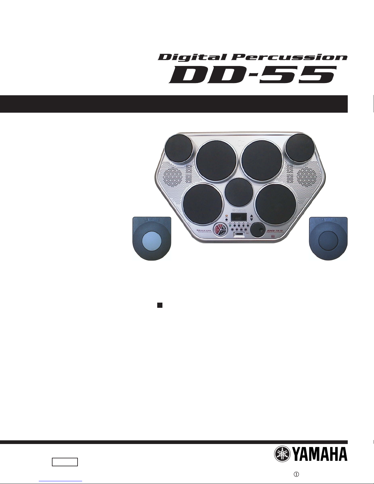
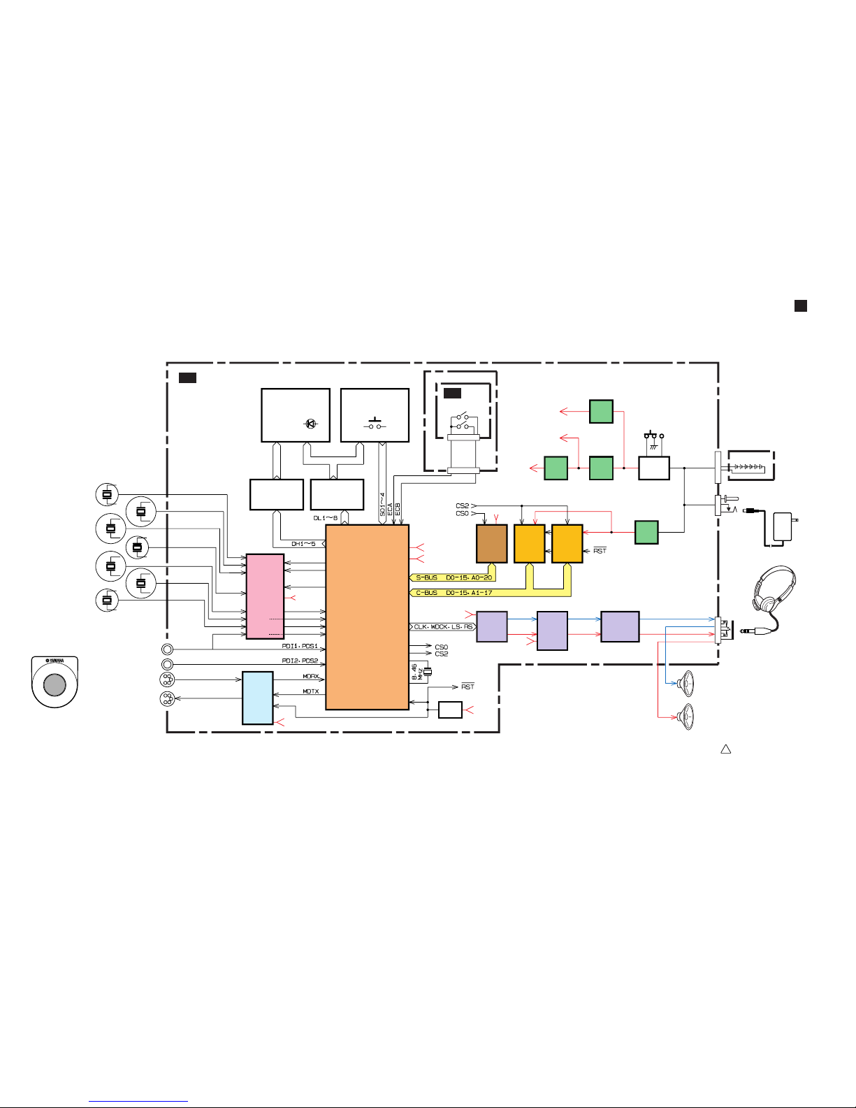
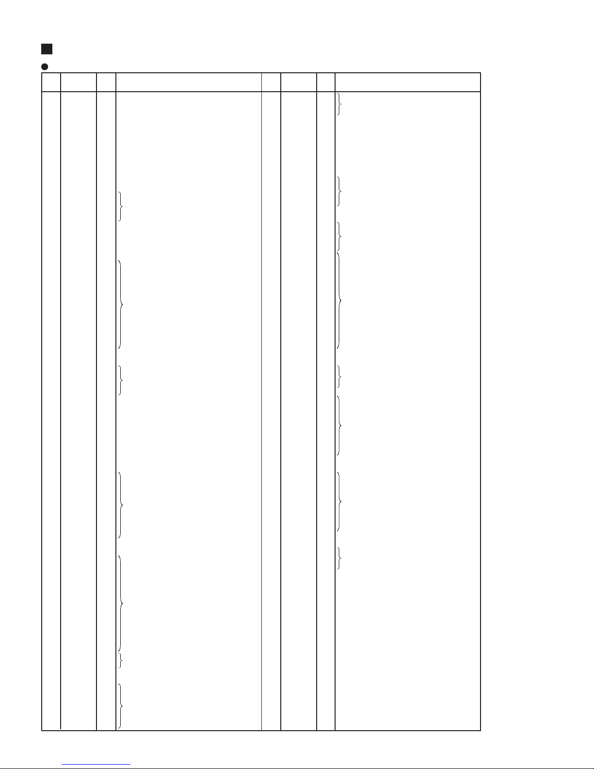
Yamaha Druid Pro DD-55 User manual

SERVICE MANUAL
HAMAMATSU, JAPAN
1.42K-0.935 K Printed in Japan 2001.05
001660
SK
CONTENTS
SPECIFICATIONS .............................................................................. 3
PANEL LAYOUT.................................................................................. 4
DIMENSION........................................................................................ 5
CIRCUIT BOARD LAYOUT................................................................. 6
BLOCK DIAGRAM .............................................................................. 7
DISASSEMBLY PROCEDURE ........................................................... 8
LSI PIN DISCRIPTION...................................................................... 10
IC BLOCK DIAGRAM.........................................................................11
CIRCUIT BOARDS ............................................................................11
TEST PROGRAM ............................................................................. 16
MIDI IMPREMENTATION CHART .................................................... 20
PARTS LIST
OVERALL CIRCUIT DIAGRAM
This document is printed on chlorine free (ECF) paper with soy ink.
PEDAL 1
PEDAL 2

2
DD-55
IMPORTANT NOTICE
This manual has been provided for the use of authorized Yamaha Retailers and their service personnel. It has been
assumed that basic service procedures inherent to the industry, and more specifically Yamaha Products, are already
known and understood by the users, and have therefore not been restated.
WARNING: Failure to follow appropriate service and safety procedures when servicing this product may
result in personal injury, destruction of expensive components and failure of the product to
perform as specified. For these reasons, we advise all Yamaha product owners that all service
required should be performed by an authorized Yamaha Retailer or the appointed service
representative.
IMPORTANT: This presentation or sale of this manual to any individual or firm does not constitute authoriza-
tion, certification, recognition of any applicable technical capabilities, or establish a principal-
agent relationship of any form.
The data provided is believed to be accurate and applicable to the unit(s) indicated on the cover. The research
engineering, and service departments of Yamaha are continually striving to improve Yamaha products. Modifications
are, therefor, inevitable and changes in specification are subject to change without notice or obligation to retrofit.
Should any discrepancy appear to exist, please contact the distributor's Service Division.
WARNING: Static discharges can destroy expensive components. Discharge any static electricity your body
may have accumulated by grounding yourself to the ground bus in the unit (heavy gauge black
wires connect to this bus).
IMPORTANT: Turn the unit OFF during disassembly and parts replacement. Recheck all work before you
apply power to the unit.
WARNING: CHEMICAL CONTENT NOTICE!
The solder used in the production of this product contains LEAD. In addition, other electrical / electronic and / or
plastic (where applicable) components may also contain traces of chemicals found by the California Health and
WelfareAgency (and possibly other entities) to cause cancer and / or birth defects or other reproductive harm.
DO NOT PLACE SOLDER, ELECTRICAL / ELECTRONIC OR PLASTIC COMPONENTS IN YOUR MOUTH FOR
ANY REASON WHAT SO EVER!
Avoid prolonged, unprotected contact between solder and your skin! When soldering, do not inhale solder fumes or
expose eyes to solder / flux vapor!
If you come in contact with solder or components located inside the enclosure of this product, wash your hands before
handling food.
WARNING
Components having special characteristics are marked and must be replaced with parts having specification equal to those originally
installed.

3
DD-55
SPECIFICATIONS
Drum Pads
7 pads (125mm x 4, 88mm x 3), Touch Sensitive
Maximum Polyphony
32
Drum Kits
45 Preset +1 Custom
Songs
100
Tracks
4 (DRUM 1/DRUM 2/DRUM 3/BACKING)
Custom Song
1 Song (approximately 20,000 notes)
Voices
Drum Voices 192 + GM Voices 128 + Drum Kits 8
Functions
Track ON/OFF, TAP START, BREAK, A-B REPEAT,DEMO
Panel Controls
[STANDBY ON / OFF] switch, [PAD] button, [KIT] button, [SONG] button, [TEMPO] button, VOLUME [ ],
[]buttons, [HAND PERC] button, TRACK (DRUM 1 / DRUM 2 /DRUM 3 / BACKING) button, [DEMO]
button, [CLICK] but-ton, [START/STOP] button, [A-B REPEAT] button, [BREAK/TAP] button, [REC] button,
DIAL
LED Display
Song / Drum Kit / Tempo etc.
Auxiliary jacks
DC IN12 V, PHONES / OUTPUT, MIDI IN / OUT, PEDAL 1/2
Oouput Impedance
33Ω (PHONES / OUTPUT jack)
Main Amplifier
5W + 5W (EIAJ)
Speaker
8 cm x 2
Power Consumption
16 W (when using PA-5C power adaptor)
Power Supply
Adaptor: DC12V (Yamaha PA-5C sold separately)
Batteries: Six “C” size, R-14(LR14), or equivalent batter-ies (sold separately)
Dimensions (WxDxH)
558 x 355 x 174 mm (22” x 14” x 6” 7/8)
Weight
3.8 kg (8 Ibs. 6 oz)
Supplied Accessories
Drum Stick x 2, Foot Pedal 1 & 2, Owner’s Manual
Optional Accessories
Headphones HPE-150

4
DD-55
PANEL LAYOUT
888
888
q
wy ut
!6
!7
!8
!2
!3
!4
!5
oi !0 !1
r
e
Front Panel
Front Panel
Pedal 2 Pedal 1
!0 SONG Button
!1 TEMPO Button
!2 START/STOP Button
!3 A-B REPEAT Button
!4 BREAK/TAP Button
!5 REC Button
!6 STANDBY/ON Switch
!7 DIAL
!8 Drum Pads (x7)
q DEMO Button
w CLICK Button
e DISPLAY.
r VOLUME [ ], [ ] Buttons
t HAND PERC Button
y DRUM 1 - 3 Buttons
u BACKING Button
i PAD Button
o KIT Button

5
DD-55
!9 @0 @1
@2
@3
@4
Side Panel L Side Panel R
Side Panel (Left)
!9 DC IN 12V (AC Adaptor) Jack
@0 PHONES/OUTPUT Jack
@1 PEDAL 2 Jack
Side Panel (Right)
@2 MIDI IN Terminal
@3 MIDI OUT Terminal
@4 PEDAL 1 Jack
558mm
173.6mm
166.8mm
354.7mm
362mm
DIMENSION

6
DD-55
CIRCUIT BOARD LAYOUT
DD 1/2
DD 2/2
Pad Assembly
Pad Assembly (L)
Speaker(L)Speaker(R) 160
U220
Upper Case
Lower Case
Top view

7
DD-55
BLOCK DIAGRAM
+5R
28CA1-8819212
MIDI
I/F
IC610
TR621
TR622
ANALOG
SWITCH
IC710,
IC750,
IC790
DAC
+5V
REG
+5V
REG
+5V
REG
+3.3V
REG
STAND BY
ON
POWER
GATE
SELECTOR
+3.3D
+3.3D
+5A
+5D
+5D
+5D
+5A
+5D
+5D
+5A
SWITCH MATRIX
17 PIECES
LED MATRIX
7seg LED 3 digit
anode common
LED Lamp
5 pieces
TRANSISTOR
ARRAY
TR411-415
DIGITAL
TRANSISTOR
TR421-428
RESET
PRE
AMP POWER
AMP
32M
ROM 1M L
SRAM1 1M H
SRAM2
SWX00B
IC100
168P
JK610
JK620
JK630
JK780
TL710,711
TL720,721
TL730,731
TL740,741
TL750,751
TL760,761
TL770,771
EC460
165
135-142
157
124
14
15
16
17
2,167
155,156
153
20
4,7,12,49,61,
77,91,148
35,119,133,
143,154,161
131
+5D
9
10
46
88
158,159,
163,164
23-34,37-40,
47,48,51-59,
62-71
80-87,89,96-99,
102-118,121-123
127-131
145-147,150
151 152
IC150-3P
13-16
1,3,4,7,8
1,9
11
6
3
7
2
8
2
7
15
14
32
30
242422 3211
1-10,14-21,
23-30,32-42 2-15,17-21,
23,25-28,31
2-15,17-21,
23,25-28,31
32
IC930-3P
IC920-4P
IC940-3P
TR930IC190-3P
12
12
13
IC710-11 IC710-5,6,12,13
IC750-5,6,12,13
IC790-5,6,12,13
IC710-8
IC710-4
IC710-1
IC750-11
IC750-8
IC750-4
IC750-1
GAT2
GAT3
GAT1
AN0
AN1
AN2
AN3
IC710,750,790-14
IC710-10
IC750-10
IC790-1
IC710-9
IC750-9
IC790-4 IC710-3
IC750-3
IC790-8
IC710-2
IC750-2
IC790-11
IC210-42P IC310-32P IC320-32P
IC500-16P IC550 IC800-18P
1
PEDAL 2 (SWITCH)
MIDI IN
MIDI OUT
SPEAKER L
SPEAKER R
PHONES/OUTPUT
BATTERY
DC IN 12V
PAD 1 SENSOR
PAD 2 SENSOR
PAD 3 SENSOR
PAD 4 SENSOR
PAD 5 SENSOR
PAD 6 SENSOR
PAD 7 SENSOR
PEDAL 1(SENSOR / SWITCH)
DD 1/2 DD 2/2
CN461 3P
CN460 3P
CN911 2P
JK850 JK901

8
DD-55
DISASSEMBLY PROCEDURE
[80]Lower Case
[60]
Upper Case
Encoder
[A]
(Fig. 1)
(Fig. 4) (Fig. 5)
(Fig. 2) (Fig. 3)
[160][160]
Lower Case
er Case
Lower Case
Soft cloth
1. Lower Case Assembly (Time required: about 2 min)
1-1 Remove the sixteen (16) screws marked [80]. The lower case assembly can then be removed. (Fig. 1)
2. DD 2/2 Circuit Board
(Time required: about 2 min)
2-1 Remove the lower case assembly. (See procedure 1.)
2-2 Remove the encoder knob marked [60]. (Fig. 4)
2-3 Remove the hexagonal nut marked [A]. The DD 2/
2 circuit board can then be removed. (Fig. 5)
* When removing the lower case, pay attention not to break [160] BAT bundled cables (see Fig. 2).
* When working with the unit turned over, place it on a soft cloth to protect the surface from scratches.
[80]: Binding Head Tapping Screw-B 3.0X12 MFZN2BL (VQ074600)
3. DD 1/2 Circuit Board
(Time required: about 4 min)
3-1 Remove the lower case assembly. (See procedure 1.)
3-2 Remove the DD 2/2 circuit board can then be
removed. (See procedure 2.)
3-3 Remove the seventeen (17) screws marked [130].
The DD 1/2 circuit board can then be removed.
(Fig. 6)
Lower CaseLower Case
ScrewScrew
(Fig. 1-1)
* In this operation, screw an easily touch and
scratch the bottom case, so be careful that
screws do not contact it.

9
DD-55
Upper Case Speaker LSpeaker R
DD 1/2
DD 2/2
[130]
[130]
[135] [135]
Pad Assembly
(Fig. 7)
(Fig. 6)
[130]: Binding Head Tapping Screw-B 3.0X8 MFZN2Y (EP600250)
[135]: Binding Head Tapping Screw-B 4.0X8 MFZN2Y (EP640410)
Upper Case
Needle-nose plyer
Upper Case
Needle-nose plyer
PAD Assembly
PAD Assembly
Pull upPull up
(Fig. 8)
4. Pad Assembly (Time required: about 5 min)
4-1 Remove the lower case assembly. (See procedure 1.)
4-2 Remove the DD 2/2 circuit board. (See procedure 2.)
4-3 Remove the DD 1/2 circuit board. (See procedure 3.)
4-4 Pull a pad assembly off the panel as shown in the
illustration. (Fig. 7)
* The pad assembly (S) and pad assembly (L) can
then be removed in the same manner.
5. Speakers (Time required: about 3 min)
5-1 Remove the lower case assembly. (See procedure 1.)
5-2 Remove the four (4) screws marked [135]. The
speakers can then be removed. (Fig. 6)
* The left speaker and right speaker can then be
removed in the same manner.
6. Attaching the Pad Assembly
6-1 Turn over the upper case and support the pad
assembly from the lower side of the case.
6-2 Insert the legs of pad assembly in the holes of the
upper case and then pull them up with a needle-
nose plyer. (Fig.8)
* All pad assemblies can be attached in the same
way.

10
DD-55
LSI PIN DISCRIPTION
HG73C205AFD (XU947C00) SWX00B TONEGENERATOR
PIN NAME I/O FUNCTION PIN NAME I/O FUNCTION
No. No.
1 ICN I Initial clear 85 CMA3 O
2 RFCLKI I PLL Clock 86 CMA8 O Program address bus
3 TM2 I PLL Control 87 CMA2 O
4 AVDD_PLL Power supply 88 CRD O read signal
5 AVSS_PLL Ground 89 CMA1 O Program address bus
6 MODE0 I SWX dual mode 90 CUB O high byte effective signal
7 VCC7 Power supply 91 VCC91 Power supply
8 GND8 Ground 92 GHND92 Ground
9 XIN I crystal oscillator 93 CS1 O CS signal
10 XOUT O crystal oscillator 94 CMA0 O Program address bus
11 MODE1 I SWX separate mode 95 CLB O low byte effective signal
12 TEST0 I TEST pin 96 CMA12 O
13 TESTON I TEST pin 97 CMA11 O Program address bus
14 AN0-P40 I 98 CMA10 O
15 AN1-P41 I A/D converter 99 CMA9 O
16 AN2-P42 I 100 GND100 Ground
17 AN3-P43 I 101 CWE O write signal
18 AVDD_AN Power supply 102 CMA16 O
19 AVSS_AN Ground 103 CMA15 O Program address bus
20 TXD0 O for MIDI or TO-HOST 104 CMA14 O
21 TXD1 O for MIDI 105 CMA13 O
22 EXCLK I Crystal oscillator 106 CMD8 I/O
23 SMD11 I/O 107 CMD7 I/O
24 SMD4 I/O 108 CMD9 I/O
25 SMD3 I/O 109 CMD6 I/O
26 SMD12 I/O 110 CMD10 I/O
27 SMD10 I/O 111 CMD5 I/O
28 SMD5 I/O Wave memory data bus 112 CMD11 I/O Program memory Data bus
29 SMD2 I/O 113 CMD4 I/O
30 SMD13 I/O 114 CMD12 I/O
31 SMD9 I/O 115 CMD3 I/O
32 SMD6 I/O 116 CMD13 I/O
33 SMD1 I/O 117 CMD2 I/O
34 SMD14 I/O 118 CMD14 I/O
35 VCC35 Power supply 119 VCC119 Power supply
36 GND36 Ground 120 GND115 Ground
37 SMD8 I/O 121 CMD1 I/O
38 SMD7 I/O Wave memory data bus 122 CMD15 I/O Program memory Data bus
39 SMD0 I/O 123 CMD0 I/O
40 SMD15 I/O 124 CMA21 O Program address bus
41 SOE O read signal 125 PDT15 I/O
42 SWE O write signal 126 PDT14 I/O
43 SRAS O RAS signal 127 PDT13 I/O
44 SCAS O CAS signal 128 PDT12 I/O SWX access data bus
45 REFRESH O REFRESH signal 129 PDT11 I/O
46 CS0 O CS signal 130 PDT10 I/O
47 SMA0 O Memory address bus 131 PDT9 I/O
48 SMA16 O 132 PDT8 I/O
49 VCC49 Power supply 133 VCC133 Power supply
50 GND50 Ground 134 GND134 Ground
51 SMA1 O 135 PDT7 I/O
52 SMA15 O 136 PDT6 I/O
53 SMA2 O 137 PDT5 I/O
54 SMA14 O 138 PDT4 I/O SWX access data bus
55 SMA3 O Memory address bus 139 PDT3 I/O
56 SMA13 O 140 PDT2 I/O
57 SMA4 O 141 PDT1 I/O
58 SMA12 O 142 PDT0 I/O
59 SMA5 O 143 VCA143 Power supply
60 GND60 Ground 144 GND144 Ground
61 VCC61 Power supply 145 PAD2 I
62 SMA11 O 146 PAD1 I SWX access address bus
63 SMA6 O 147 PAD0 I
64 SMA10 O 148 VCC148 Power supply
65 SMA7 O 149 GND149 Ground
66 SMA9 O 150 PCS I Chip select
67 SMA17 O 151 PWR I write enable
68 SMA8 O Memory address bus 152 PRD I read enable
69 SMA18 O 153 RXD0 I for Midi or TO-HOST
70 SMA19 O 154 RXD1 I for Midi or Key scan
71 SMA20 O 155 SCLKI I EXT Clock
72 SMA21 O 156 ADIN I A/D converter
73 SMA22 O 157 ADLR O A/D converter LR clock
74 SMA23 O 158 DO0 O DAC
75 CMA20 O Program address bus 159 DO1 O DAC
76 CMA19 O 160 SYSCLK O 1/2 clock
77 VCC77 Power supply 161 VCC161 Power supply
78 GND78 O Ground 162 GND162 Ground
79 CMA18 O 163 WCLK O for DAC LR clock
80 CMA17 O 164 QCLK O 1/12 clock
81 CMA5 O Program address bus 165 BCLK O IIS-DAC clock
82 CMA6 O 166 SYI I Synch signal
83 CMA4 O 167 IRQ0 I Interrupt request
84 CMA7 O 168 NMI I Interrupt request
DD 1/2: IC100

11
DD-55
IC BLOCK DIAGRAM
uPD63200GS (XM145A00) DAC (Digital to Analog Converter)
PIN NAME I/O FUNCTION PIN NAME I/O FUNCTION
No. No.
1 4/8F I 4/8 Fs selection 9 R. REF Channel R voltage reference
2 D. GND Digital ground 10 L. REF Channel L voltage reference
3 16 BIT I 16 bit/18 bit selection 11 L. OUT O Channel L output
4 D. VDD Digital power supply 12 A. GND Analog ground
5 A. GND Analog ground 13 WDCK I Word clock
6 R. OUT O Channel R output 14 RSI I Channel R series input
7 A. VDD Analog power supply 15 SI/LSI I Series input/Channel L series input
8 A. VDD 16 CLK I Clock
1
2
3
4
5
6
7
13
12
11
10
9
8
141A
1B
2B
2A
2C
3C
GND
Vcc
1C
4C
4A
4B
3B
3A
SN74HC4066NSR (XZ824A00)
HD74HC4066NSR (X0563A00)
ANALOG SWITCH
1
A
23456789
+V IN V
+INOUT +VIN
+IN OUT
+
B
+
uPC4572HA (XF633A00)
OP AMP
DD 1/2: IC500
DD 1/2: IC710
IC750
IC790
DD 1/2: IC550
Encoder
to DD 1/2 CN461
DD 2/2 Circuit Board
Component Side Pattern Side
DD 2/2: 2NA-V707790
1
CIRCUIT BOARDS

12
DD-55
A
A’
MIDI INMIDI OUTPEDAL 1
to DD 2/2 CN460
DD 1/2 Circuit Board (Component Side)
Component Side DD 1/2: 2NA-V707790
1

13
DD-55
to Battery to Speaker L, R
DC IN 12V PHONES/OUTPUT PEDAL 2
A
A’Component Side
DD 1/2: 2NA-V707790
1

14
DD-55
PAD 1 PAD 2
DEMO
CLOCK
REC BREAK
/TAP
A-B
REPEAT
START
/STOP
HAND
PERC
DRUM1 DRUM2
PAD KIT
A
A’
DD 1/2 Circuit Board (Pattern Side)
Pattern Side DD 1/2: 2NA-V707790
1

15
DD-55
PAD 3 PAD 4 PAD 5 PAD 6 PAD 7
VOLUME
BACKING
TEMPO
DRUM3DRUM2
SONGKIT
STANDBY/ON
A
A’Pattern Side
DD 1/2: 2NA-V707790
1

16
DD-55
TEST PROGRAM
(Fig. 1)
(Fig. 2)
(Fig. 3)
PushPush
ONON
Setting Conditions
Requirements for Measurement
Before starting to measure the unit, make sure you have the following instrumentations and test jigs:
Measuring instruments:
Oscilloscope (Input impedance, 1M Ωor more; Loading, 33 Ω)
Level indicator (JIS-C curve; Input impedance, 1M Ωor more; Loading, 33 Ω; 0dBm: 1mW 600 Ω)
Test jigs:
Power adaptor, PA-5C
Stick
A. Setting Conditions
Set the [STANDBY/ON] switch to ON with the [TEMPO] and [HANDPERC] button pressed and held (Fig. 1).
B. Test Entry
To scroll the test items, press the [VOLUME ] button for forwards, and the
[VOLUME ] for backwards.
To start a test, press the [START/STOP] button.
Pressing the [START/STOP] button again returns to the selected item.
If you pass the test and return to the selected item, a dot appears on the upper left
of the LED segment (See Fig.2).
If you fail the test, the LED shows “Err”(See Fig.3). To return to the selected
item, press the [DEMO] button. (Note that the [START/STOP] button is inactive
at this time.)
* Even if the test has successfully completed, pressing the [DEMO] button forces
the system back to the Item Selection.
* The LED displays, and/or the interactions for OK/NG may be different depending
on the test types. For details, see each test item you want to perform.
C. Step for NG
If the unit could not pass a test press the [DEMO] button to display the “Test Item
Selection”screen.
(Note that the [START/STOP] button is inactive at this time.)

17
DD-55
5. Test Items
Test No. LED display Test function and judgment criteria
1001: Version Displays version for ROM.
ROM versions are displayed alternately in the LED.
[Displaying the test result]
OK, X'XX: ["XX"]
NG: ["Err"]
2002: Rom Check 1 Checks the ROM.
The test result appears on the LED.
[Displaying the test result]
OK: ["PAS"]
NG: ["Err"]
3003: Ram Check 1 Checks all RAMs which are connected to the CPU.
The test result appears on the LED.
[Displaying the test result]
OK: ["PAS"]
NG: ["Err"]
11 011: TG1 Check Output the sine wave by changing the channels in sequence from C2 to G4.
After autoscaling is finished, individual keys can be played.
Check to see if there is no abnormal noie or tone.
13 013: Pitch Check Checks the Pitch.
Connect the frequency counter to the [PHONES/OUTPUT] jack.
Check that the 440.0 +/-1.76 Hz signal is output.
14 014: Output R Check Connect the level meter (with a JIS-C filter) to the [PHONES/OUTPUT] jack.
(Load: 33 ohm)
PHONES L: Less than -60.0 dBm
PHONES R: -11.5 dBm +/-2
15 015: Output L Check Connect the level meter (with a JIS-C filter) to the [PHONES/OUTPUT] jack.
(Load: 33 ohm)
PHONES R: Less than -60.0 dBm
PHONES L: -11.5 dBm +/-2 dB
19 019: Noise Level Check Connect the level meter (with a JIS-C Filter) to the [PHONES/OUTPUT] jack.
(Load: 33 ohm)
Phones L/R: Less than -80.0 dBm
20 020:
Switch and LED Check
Check switches on the panel and LED.
Press the switches which are displayed on the LED.
A pre-assigned note is output when depressing the switch.
The test result appears on the LED. (Table 1)
[Displaying the test result]
OK: ["PAS"]
NG: ["Err"]
21 021: Panel LED Check Checks the panel LED.
As the test is started, all the LED's go on.

18
DD-55
30 030: Pad Check Checks the PAD.
When a pad is tapped, the LED's indicate its identification number and tapping
power.
[Displaying the test result]
Maximum data: 7F
Minimum data: 18
31 031: Pedal 1 Check Checks the [PEDAL 1].
Connect the pedal to the [PEDAL 1] jack. When the pedal is stepped on, it
sounds in bass drum tones. The LED's indicate the tapping power.
[Displaying the test result]
Maximum data: 7F
Minimum data: 38
32 032: Pedal 2 Check Checks the [PEDAL 2].
Connect the pedal to the [PEDAL 2] jack.
Check that the C3 note is output when starting the test program.
Check that the C4 note is output when pushing the pedal and that tone is turned
off when releasing the pedal.
"20F" is displayed and the sound stops.
37 037: MIDI Check Checks the MIDI.
After connecting the [MIDI IN] and [MIDI OUT] with a MIDI cable, execute
the test.
Check that the C4 note is output and the test result appears on the LED.
[Displaying the test result]
OK: ["PAS"]
NG: ["Err"]
41 041: Rom 2 Check Checks the ROM.
The test result appears on the LED.
[Displaying the test result]
OK: ["PAS"]
NG: ["Err"]
42 042: Ram 2 Check Checks the RAM.
The test result appears on the LED.
[Displaying the test result]
OK: ["PAS"]
NG: ["Err"]
46 046: Rom Backup Performs the RAM back-up check.
Check 2 After checking that the beginning becomes NG, turn the power switch off.
Enter the test program and perform the RAM back-up and check again.
[Displaying the test result]
OK: ["PAS"]
NG: ["Err"]
---: Factory Set All RAMs are initialized and set to the factory preset date when executing this
test. Set the [STANDBY/ON] switch to ON with the [DEMO] button pressed
and held.
Turn the power off.

19
DD-55
Table 1. SW test Item
No SW Display Note No SW Display Note
1 A-B REPEAT S01 C2 10 HI-HAT S10 A2
2 START/STOP S02 C#2 11 BACKING S11 A#2
3 REC S03 D2 12 PAD S12 B2
4 BRAKE/TAP S04 D#2 13 KIT S13 C3
5 DEMO S05 E2 14 SONG S14 C#3
6 CLICK S06 F2 15 TEMPO S15 D3
7 HAND PERC. S07 F#2 16 VOLUME S16 D#3
8 BASS S08 G2 17 VOLUME S17 E3
9 SNARE S09 G#2 18 DIAL O** F3

20
DD-55
MIDI IMPREMENTATION CHART
YAMAHA [ DIGITAL PERCUSSION ] Date:07-FEB-2001
Model DD-55 MIDI Implementation Chart Version : 1.0
Transmitted Recognized Remarks
Function...
Basic Default 1O - 16 1 - 16
Channel Changed 1 - 16 1 - 16
Default 3 3
Mode Messages x x
Altered ************** x
Note 0 - 127 13 - 96
Number : True voice ************** 13 - 96
Velocity Note ON o 9nH,v=1-127 o 9nH,v=1-127
Note OFF o 9nH,v=0 o 9nH,v=0
After Key's x x
Touch Ch's x x
Pitch Bend o *3 o
Prog o o 0 - 127
Change : True # **************
System Exclusive o *4 o *4
: Song Pos. x x
Common : Song Sel. x x
: Tune x x
System : Clock o o
Real Time: Commands o o *2
Aux :All Sound OFF x o(120)
:Reset All Cntrls x o(121)
:Local ON/OFF x x
:All Notes OFF x x
Mes- :Active Sense o o
sages:Reset x x
Mode 1 : OMNI ON , POLY Mode 2 : OMNI ON ,MONO o : Yes
Mode 3 : OMNI OFF, POLY Mode 4 : OMNI OFF,MONO x : No
0,32 o o Bank Select
1 o *3 o Modulation
6,38 o *3 o Data Entry
7 o o Volume
10 o *1 o Pan
11 o o Expression
Control 64 o *3 o Sustain
71 o *3 o Harmonic Content
72 o *3 o Release Time
Change 73 o *3 o Brightness
84 o *3 o Portament Cntrl
91 o o Reverb Depth
93 o *3 o Chorus Depth
94 o *3 o Variation Depth
96,97 o *3 o Data Inc,Dec
100,101 o *3 o RPN LSB,MSB
Other manuals for Druid Pro DD-55
2
Table of contents
Other Yamaha Drum manuals

Yamaha
Yamaha Electronic Drum Set HXR4LD User manual

Yamaha
Yamaha KU100 User manual

Yamaha
Yamaha PCY135 User manual

Yamaha
Yamaha KP100 User manual

Yamaha
Yamaha KU100 User manual

Yamaha
Yamaha MOTIF XF User manual

Yamaha
Yamaha XP105T-X User manual

Yamaha
Yamaha DD-9 User manual

Yamaha
Yamaha JUNIOR KIT User manual

Yamaha
Yamaha RY30 User manual

Yamaha
Yamaha DTX Drums TP70S User manual

Yamaha
Yamaha DD-75 Service manual

Yamaha
Yamaha DTXTREME User manual

Yamaha
Yamaha DD65 YDD-60

Yamaha
Yamaha RS-75 Installation guide

Yamaha
Yamaha RX 5 Quick start guide

Yamaha
Yamaha YDD-60 User manual

Yamaha
Yamaha DTX-MULTI User manual

Yamaha
Yamaha ED10 User manual

Yamaha
Yamaha RS-100 Installation guide