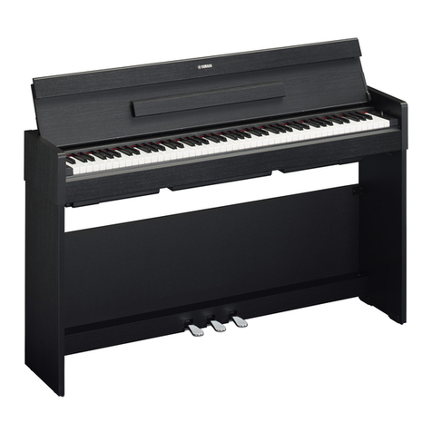
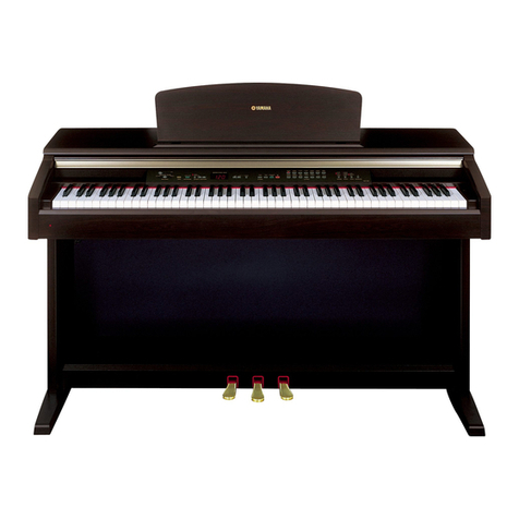
Yamaha YDO-323 User manual

SERVICE MANUAL
■CONTENTS
SPECIFICATIONS..................................................................... 3
PANEL LAYOUT....................................................................... 4
DISASSEMBLY PROCEDURE ................................................. 5
LSI PIN DESCRIPTION........................................................... 15
IC BLOCK DIAGRAM ............................................................. 17
CIRCUIT BOARDS.................................................................. 18
TEST PROGRAM ................................................................... 27
BACKING UP DATA AND INITIALIZING THE SETTINGS ....
32
TRANSMITTING SONG DATA BETWEEN THE COMPUTER
AND YDP-323 .......................................................................
33
MIDI IMPLEMENTATION CHART.......................................... 34
MIDI DATA FORMAT ............................................................. 35
PARTS LIST
BLOCK DIAGRAM
CIRCUIT BOARD LAYOUT & WIRING
OVERALL CIRCUIT DIAGRAM
Copyright (c) Yamaha Corporation. All rights reserved. PDF-K7901 ’05.10
PK 001744

YDP-323
2
IMPORTANT NOTICE
This manual has been provided for the use of authorizedYamaha Retailers and their service personnel.It has been assumed
that basic service procedures inherent to the industry, and more specifically Yamaha Products, are already known and
understood by the users, and have therefore not been restated.
WARNING : Failure to follow appropriate service and safety procedures when servicing this product may result in
personal injury, destruction of expensive components and failure of the product to perform as
specified. For these reasons, we advise all Yamaha product owners that all service required should
be performed by an authorizedYamaha Retailer or the appointed service representative.
IMPORTANT : This presentation or sale of this manual to any individual or firm does not constitute authorization,
certification, recognition of any applicable technical capabilities, or establish a principal-agent
relationship of any form.
The data provided is believed to be accurate and applicable to the unit (s) indicated on the cover.The research engineering,
and service departments ofYamaha are continually striving to improveYamaha products.Modifications are, therefore, inevitable
and changes in specification are subject to change without notice or obligation to retrofit. Should any discrepancy appear to
exist, please contact the distributor’s Service Division.
WARNING : Static discharges can destroy expensive components. Discharge any static electricity your body
may have accumulated by grounding yourself to the ground bus in the unit (heavy gauge black wires
connect to this bus).
IMPORTANT : Turn the unit OFF during disassembly and parts replacement. Recheck all work before you apply
power to the unit.
WARNING : CHEMICAL CONTENT NOTICE !
The solder used in the production of this product contains LEAD. In addition, other electrical/electronic and/or plastic (where
applicable) components may also contain traces of chemicals found by the California Health and Welfare Agency (and
possibly other entities) to cause cancer and/or birth defects or other reproductive harm.
DO NOT PLACE SOLDER, ELECTRICAL/ELECTRONIC OR PLASTIC COMPONENTS IN YOUR MOUTH FOR ANY
REASON WHAT SO EVER!
Avoid prolonged, unprotected contact between solder and your skin! When soldering, do not inhale solder fumes or expose
eyes to solder/flux vapor!
If you come in contact with solder or components located inside the enclosure of this product, wash your hands before
handling food.
■WARNING
Components having special characteristics are marked Zand must be replaced with parts having specification equal to
those originally installed.
■SAVING DATA
Saving and backing up your data
• Data in the instrument’s internal memory can be lost due to operational errors or malfunction. Be sure to save any important
data to external media via a computer connected to the instrument.

YDP-323
3
■SPECIFICATIONS
Item
Keyboard
Sound Source
Polyphony
Voice Selection
Effect
Volume
Controls
Pedal
Demo Songs
Recording Function
Loading song data from
a computer
Jacks/Connectors
Main Amplifiers
Speakers
Dimensions (W x D x H)
(with music rest)
Weight
Accessories
YDP-323
88 keys (A-1 - C7)
AWM Stereo Sampling
64 Notes Max.
10
Reverb
Master Volume
Dual, Metoronome, Transpose
Damper, Sostenuto, Soft
10 Demo Songs, 50 Piano Preset Songs
One song 65 KB (approx. 11,000 notes)
Up to 10 songs;Total maximum size 352 KB
MIDI (IN/OUT), PHONES x 2
20W x 2
Oval (12cm x 6cm) x 2
1357mm x 420mm x 814mm [53-3/8" x 16-1/2" x 32-1/16"]
(1357mm x 420mm x 987mm [53-3/8" x 16-1/2" x 38-7/8"])
41kg (90lbs., 6oz)
Owner’s Manual, “50 greats for the Piano”(Music Book), Bench (included or optional depending
on locale), Quick Operation Guide, Headphone hanger set, AC cord, Assembly parts
●Options
BC-100 Bench
UX16 (USB-MIDI interface)

YDP-323
4
■PANEL LAYOUT
MIDI
INOUT
PHONES
PEDAL
POWER
0 A
1
2
B
C
D
9
3
4
5
6
7
8
YDP-323
1[POWER] switch
2[DEMO/SONG] button
3[PIANO/VOICE] button
4[SELECT] button
5[REC] button
6[PLAY] button
7[METRONOME] button
8[MASTER VOLUME] dial
9[PHONES] jacks
0MIDI [IN] [OUT] terminals
A[PEDAL] terminal
BSoft pedal (left)
CSostenuto pedal (center)
DDamper pedal (right)

YDP-323
5
2. Music Rest Assembly
(Time required: About 1 minute)
Remove the four (4) screws marked [S10]. The music
rest assembly can then be removed. (Fig. 2)
■DISASSEMBLY PROCEDURE
Fig. 1
[11b]: TrussHeadScrew4.0X10MFZN2BL(WF000800)
1. Headphone Hanger
(Time required: About 1 minute)
Remove the two (2) screws marked [11b]. The
headphone hanger can then be removed. (Fig. 1)
Fig. 2
[
S10]: BindHeadTappingScrew-13.0X16MFZN2B3(WE971200)
3. Top Board Assembly
(Time required: About 1 minute)
3-1 Close the key cover.
3-2 Remove the three (3) screws marked [S09]. (Fig. 3)
3-3 Slide the top board assembly forward and lift it out.
Caution:
Be sure to attach the removed filament tape just as it was
before removal.
4. Back Board (Time required: About 1 minute)
Remove the screw marked [5bA], the screw marked
[5bB] and the four (4) screws marked [5d]. The back
board can then be removed. (Fig. 3)
PHONES
[11b]
Headphone hanger
[5b]: TrussHeadScrew4.0X12MFZN2B3(WE997700)
[5d]: PWHeadTappingScrew-14.0X20MFZN2B3(WE998900)
[S09]: TrussHeadScrew4.0X16MFZN2B3(WE977600)
Fig. 3
<Rear view>
K K K K
Music rest assembly
[S10]
[S10]
[S09] [S09]
[5bB]
[5bA]
[5d]
[5d]
Top board assembly
Back board
Side board assembly R
Side board assembly L

YDP-323
6
●Power Supply Unit
Fig. 5
[1]:
BindHeadTappingScrew-B3.0X10MFZN2B3(WE972200)
[6]:
BindHeadTappingScrew-B3.0X12MFZN2W3(WE987400)
[7A]:
BindHeadTappingScrew-B4.0X10MFZN2B3(WE972300)
6. PS Circuit Board, PowerTransformer
(Time required: About 5 minutes)
6-1 Remove the top board assembly. (See procedure 3)
6-2 Remove the power supply unit. (See procedure 5)
6-3 Remove the three (3) screws marked [6], the two (2)
screws marked [7A] and the two (2) screws marked
[1]. The PS circuit board can then be removed from
the AC inlet plate. (Fig. 5)
6-4 PowerTransformer
Using the soldering iron, remove the seventeen
soldered place of the power transformer on the PS
circuit board. The power transformer can then be
removed from the PS circuit board. (Fig. 5-1)
* While soldering, be careful not to apply too much heat.
It might cause peeling off the land pattern.
Fig. 4
5. Circuit Boards & Assemblies (Main Unit)
(Time required: About 3 minutes each)
5-1 Remove the top board assembly. (See procedure 3)
5-2 Each circuit board and assembly can be removed by
removing its fixing screws as listed below.
Circuit board and Assembly Ref. No. Screw QTY Fig.
DM S12A Bind Head Tapping Screw-B 3.0X6 MFZN2W3 (WE936300) 4 4
MAEQ S12B Bind Head Tapping Screw-B 3.0X6 MFZN2W3 (WE936300) 6 4
PS Cover Assembly 103A Bind Head Tapping Screw-1 3.5X12 MFZN2W3 (WE970900) 5 4
Power Supply Unit 103B Bind Head Tapping Screw-1 3.5X12 MFZN2W3 (WE970900) 3 4
D-JACK Assembly S13A Bind Head Tapping Screw-1 3.5X12 MFZN2W3 (WE970900) 4 4
Speaker L S07A Truss Head Tapping Screw-1 4.0X16 MFZN2Y (WE965700) 4 4
Speaker R S07B Truss Head Tapping Screw-1 4.0X16 MFZN2Y (WE965700) 4 4
[103A]
[103A]
[103B] [103A]
Power supply assembly
PS cover assembly
DM MAEQ
[S07A] [S13A] [S12A] [S12B]
Speaker L Speaker R
D-JACK assembly
DM MAEQ
[S12A] [S12B]
[S07B][S07B]
AC inlet plate
Power transformer
[6] [6]
[1]
[6]
[7A]
PS

YDP-323
7
7. DJACK Circuit Board
(Time required: About 3 minutes)
7-1 Remove the top board assembly. (See procedure 3)
7-2 Remove the D-JACK assembly. (See procedure 5)
7-3 Remove the three (3) screws marked [3A] and the two
(2) screws marked [4]. The DJACK circuit board can
then be removed from the D-JACK angle. (Fig. 6)
Fig. 5-1
●D-JACK Assembly
[3A]: BindHeadTappingScrew-B3.0X8MFZN2B3(WE774400)
[4]: BindHeadTappingScrew-B3.0X8MFZN2W3(WE774300)
Fig. 6
Solder
(Pattern side)
PS
<Bottom view>
8. Key Cover Assembly
(Time required: About 2 minutes)
8-1 Close the key cover.
8-2 Remove the top board assembly. (See procedure 3)
8-3 Lift the rear key cover assembly. (Fig. 7)
8-4 Lean slightly the key cover assembly so that the guide
pin can be removed from the guide rail. (Fig. 7-1)
* When removing, be sure not to nake scratches on the
side cover.
* When reinstalling the key cover assembly, apply a
masking shield tape around the guide rail to prevent
from making scratches on the assembly.
Fig. 7
Fig. 7-1
[3A] D-JACK angle
[4]
DJACK
Key cover assembly
Key cover assembly
Guide pin
Guide rail

YDP-323
8
10. Stopper Rail Assembly
(Time required: About 5 minutes)
10-1 Remove the top board assembly. (See procedure 3)
10-2 Remove the key cover assembly. (See procedure 8)
10-3 Remove the rack L and R. (See procedure 9)
10-4 Remove the two (2) screws marked [S13B] each from
both sides of the assembly. (Fig. 8)
10-5 Remove the six (6) screws marked [S13C] .The stopper
rail assembly can then be removed. (Fig. 9)
11. End Block Assembly (L, R)
(Time required: About 5 minutes)
11-1 Remove the top board assembly. (See procedure 3)
11-2 Remove the key cover assembly. (See procedure 8)
11-3 Remove the rack L and R. (See procedure 9)
11-4 Remove the stopper rail assembly. (See procedure 10)
11-5 Remove the screw marked [S08]. (Fig. 9)
11-6 Slide the end block assembly L backward and lift it
out.
* The left and right end block assembly can then be
removed in the same manner.
12. Keyboard Assembly
(Time required: About 10 minutes)
12-1 Remove the top board assembly. (See procedure 3)
12-2 Remove the key cover assembly. (See procedure 8)
12-3 Remove the rack L and R. (See procedure 9)
12-4 Remove the stopper rail assembly. (See procedure 10)
12-5 Remove the end block assembly L and R.
(See procedure 11)
12-6 Remove the nine (9) screws marked [S01] and the two
(2) screws marked [S02]. The keyboard assembly can
then be removed. (Fig. 9)
[S01]: PanHeadScrew5.0X25MFZN2W3SW(WF001500)
[S02]: BindHeadTappingScrew-14.0X14MFZN2W3(WE971900)
[S08]: BindHeadTappingScrew-B4.0X10MFZN2W3(WE974500)
[S13C]: BindHeadTappingScrew-13.5X12MFZN2W3(WE970900)
9. Rack (L, R)
(Time required: About 3 minutes each)
9-1 Remove the top board assembly. (See procedure 3)
9-2 Remove the key cover assembly. (See procedure 8)
9-3 Remove the three (3) screws marked [S06]. The rack
L can then be removed. (Fig. 8)
* The left and right rack can then be removed in the same
manner.
[S03]: BindHeadTappingScrew-13.5X16MFZN2W3(WE970700)
[S04A]: TrussHeadTappingScrew-13.5X25MFZN2W3(WE970200)
[S06]: BindHeadTappingScrew-13.5X20MFZN2W3(WE971500)
[S13B]: BindHeadTappingScrew-13.5X12MFZN2W3(WE970900)
Fig. 8
<Left side view>
Fig. 9
N
N
F
F
F
Rack L
Guide rail L
[S06] [S06]
[S03]
[S04A]
[S13B]
Stopper rail
assembly Back top board
assembly
Arm
assembly L
[S01] [S01] [S01][S13C] [S01]
Stopper rail assembly
[S13C][S08]
End block assembly L [S02]
[S13C]
End block assembly R
Keyboard assembly
[S02]

YDP-323
9
13.
MVR Circuit Board, PANEL Circuit Board
(Time required: About 7 minutes each)
13-1 Remove the top board assembly. (See procedure 3)
13-2 Remove the key cover assembly. (See procedure 8)
13-3 Remove the rack L and R. (See procedure 9)
13-4 Remove the stopper rail assembly. (See procedure 10)
13-5 Remove the end block assembly L. (See procedure 11)
13-6 MVR Circuit Board
Remove the three (3) screws marked [9A]. The MVR
circuit board can then be removed. (Fig. 10)
13-7 PANEL Circuit Board
Remove the six (6) screws marked [9B]. The PANEL
circuit board can then be removed. (Fig. 10)
Fig. 10
●End Block Assembly L
[9]: BindHeadTappingScrew-B3.0X8MFZN2W3(WE774300)
14. Power Switch Assembly
(Time required: About 7 minutes)
14-1 Remove the top board assembly. (See procedure 3)
14-2 Remove the key cover assembly. (See procedure 8)
14-3 Remove the rack L and R. (See procedure 9)
14-4 Remove the stopper rail assembly. (See procedure 10)
14-5
Remove the end block assembly R. (See procedure 11)
14-6 Remove the two (2) screws marked [30]. The power
switch assembly can then be removed. (Fig. 11)
Fig. 11
●End Block Assembly R
[30]: BindHeadTappingScrew-B3.0X8MFZN2W3(WE774300)
15. HP Circuit Board
(Time required: About 6 minutes)
15-1 Remove the top board assembly. (See procedure 3)
15-2 Remove the key cover assembly. (See procedure 8)
15-3 Remove the rack L and R. (See procedure 9)
15-4 Remove the stopper rail assembly. (See procedure 10)
15-5
Remove the end block assembly L. (See procedure 11)
15-6 Remove the two (2) hexagonal nuts marked [3B]. The
HP circuit board can then be removed. (Fig. 12)
Fig. 12
[3B]: HexagonalNut12X14X2P=1.0(WF559900)
Fig. 13
[T2f]: BindHeadTappingScrew-13.5X12MFZN2W3(WE970900)
16. PL Circuit Board
(Time required: About 10 minutes)
16-1 Remove the top board assembly. (See procedure 3)
16-2 Remove the key cover assembly. (See procedure 8)
16-3 Remove the rack L and R. (See procedure 9)
16-4 Remove the stopper rail assembly. (See procedure 10)
16-5 Remove the end block assembly L and R.
(See procedure 11)
16-6 Remove the keyboard assembly. (See procedure 12)
16-7 Remove the screw marked [T2f]. The PL circuit board
can then be removed. (Fig. 13)
[30]
Power switch assembly
[9B] [9B] [9A]
MVRPANEL
●Bottom view
[3B]
HP
PL
[T2f]
Arm assembly L

YDP-323
10
Fig. 14
[S04]: TrussHeadTappingScrew-13.5X25MFZN2W3(WE970200)
Fig. 16
Fig. 15
[5c]: BindHeadScrew6.0X16MFZN2B3(WE969400)
<Bottom view>
18. Main Unit
(Time required: About 3 minutes)
18-1 Spread a soft cloth like a blanket on the floor where
the main unit is to be placed in advance.
18-2 Remove the headphone hanger. (See procedure 1)
18-3 Disconnect the AC cord and the PK-LF cable.
(Fig. 15)
18-4 Remove the four (4) screws marked [5c]. (Fig. 16)
18-5 Move the main unit backward, lift it and place it on
the cloth gently. (Fig. 17)
* For safety, this work should be done by two persons.
17. BackTop Board Assembly
(Time required: About 3 minutes)
17-1 Remove the top board assembly. (See procedure 3)
17-2 Remove the two (2) screws marked [S04A] each from
both sides of the assembly. (Fig. 8)
17-3 Remove the six (6) screws marked [S04B]. The back
top board assembly can then be removed. (Fig. 14)
Arm assembly L Keybed assembly
[S04C]
[S04B] [S04B]
Arm assembly R
Back Top assembly
ACINLET
PEDAL
PK-LF cable
AC cord
[5c]

YDP-323
11
Fig. 17
19. Arm Assembly (L, R)
(Time required: About 15 minutes)
19-1 Remove the top board assembly. (See procedure 3)
18-2 Remove the key cover assembly. (See procedure 8)
19-3 Remove the rack L and R. (See procedure 9)
19-4 Remove the stopper rail assembly. (See procedure 10)
19-5 Remove the end block assembly L and R.
(See procedure 11)
19-6 Remove the keyboard assembly. (See procedure 12)
19-7 Remove the main unit. (See procedure 18)
(Parts removed in Steps 19-1 through 19-6 are
component parts of the main unit.)
19-8 Remove the two (2) screws marked [S04A] and the
tow (2) screws marked [S03]. (Fig. 8)
19-9 Remove the three (3) screws marked [S04C]. The arm
assembly L can then be removed. (Fig. 14)
* The arm assembly R can then be removed in the same
manner.
20. Side Board Assemble (L, R)
(Time required: About 4 minutes)
20-1 Remove the headphone hanger. (See procedure 1)
20-2 Disconnect the AC cord and the PK-LF cable.
(Fig. 15)
20-3 Remove the main unit. (See procedure 18)
20-4 Remove the screw marked [5bA] and the two (2)
screws marked [5a]. The side board assembly L can
then be removed. (Fig. 3, 18)
* The side board assembly R can then be removed in
the same manner.
Fig. 18
[5a]: TrussHeadScrew6.0X20MFZN2B3(WF001300)
Hold here. Do not hold here.
ZCAUTION
Do not hold the key cover or top portion.
For safety, this work should be done by two persons.
Do not hold here.
Key cover
Top portion
21. Stand Base (Time required:About 3 minutes)
21-1 With a soft cloth like a blanket placed on the floor,
place the main unit on its back board gently.
* For safety, this work should be done by two persons.
21-2 Put thick books or the like under the main unit at both
sides.
21-3 Remove the three (3) screws marked [3C]. The left
stand base can then be removed. (Fig. 19)
* The right stand base can then be removed in the same
manner.
Fig. 19
[3C]: PanHeadTappingScrew-14.0X65MFZN2W3(WF514200)
22. Pedal Box Assembly, Pedal Assembly
(Time required: About 5 minutes)
22-1 Disconnect the PK-LF cable. (Fig. 15)
22-2 Remove the four (4) screws marked [5d]. (Fig. 3)
22-3 Remove the two (2) screws marked [5a] each from
both sides of the assembly. The pedal box assembly
can then be removed. (Fig. 18)
22-4 Remove the eight (8) screws marked [7B] and the
screw marked [8]. The pedal assembly can then be
removed. (Fig. 20)
[5a]
Side board assembly L
Pedal box assembly
[3C]
Stand base

YDP-323
12
GHD EBUS LGHD MGHD H
[260C] [260B] [260A]
[262]
MK SUB
[260]: Bind Head Tapping Screw-P 3.0x10 MFZN2 (VT413400) or
Bind Head Tapping Screw-P 3.0x10 MFZN2W3 (WF001000)
[262]: PW Head Tapping Screw-P 3.0x10⁻¹⁰ ZMC2W3 (WF765500)
23-1 GHD EBUS L, MK SUB Circuit Board
Remove the seven (7) screws marked [260A]. The
GHD EBUS L and MK SUB circuit boards can then
be removed. (Fig. 22, 22-1)
23-2 GHD M Circuit Board
Remove the five (5) screws marked [260B] and the
screw marked [262]. The GHD M circuit board can
then be removed. (Fig. 22)
23-3 GHD H Circuit Board
Remove the four (4) screws marked [260C] and the
screw marked [262]. The GHD H circuit board can
then be removed. (Fig. 22)
* Keys can be removed without removing the circuit
boards.
* After removing the GHD EBUS L, GHD M and GHD H
circuit boards, and the rubbers can then be removed.
Fig. 22-1
MK SUB GHD EBUS L
Fig. 22
●Pedal Box Assembly
[7B]: BindHeadTappingScrew-14.0X14MFZN2W3(WE971900)
[8]: TrussHeadTappingScrew-14.0X12MFZN2W3(WF745900)
Fig. 20
23. Disassembling the Keyboard
* After inserting a round stick (Rod:TX000670) between
the frame and the keys, remove the circuit boards.
(Fig. 21)
Round stick
(Rod:TX000670)
Fig. 21
[7B] [7B] [8]
[7B][7B]
Pedal assembly

YDP-323
13
23-4 Rubber contact
Remove the GHD circuit board for the involved key.
The rubber contacts can then be removed. (Fig. 23,
24)
GHD EBUS L
Fig. 23 Fig. 24
Rubber contact Rubber contact
23-5 White key
In order to release the white key from the stopper, insert
a thin plate between the white keys (gap in the direction
indicated by the triangle mark, near the fulcrum of the
key), press down the stopper marked [A] and move
the white key forward. Then the white key being
released from the stopper lifts up. (Fig. 25, 26)
* Use special care not to move the white key forward so
much as to cause damage to the key spring.
23-6 In this state, move the white key rearward a little. Then
the white key can be removed. (Fig. 26)
23-7 Black key
The black key can be removed after the white keys on
either side have been removed.
Fig. 25 Fig. 26
23-8 Hammer,White Key
After a key has been removed, push a key spring down
once to take it out of the hook. (Fig. 27)
Place the keyboard assembly upside-down and peel
the stopper away. The hammer of the white key can
then be removed. (Fig. 28)
* The hammer of the black key can then be removed in
the same manner.
Fig. 27 Fig. 28
Thin metal plate etc
Triangle mark
[A] Spring
White key
Spring
Hook
Hammer, white key
Stopper (L88_W)

YDP-323
14
24-2 Spring
Place the keyboard assembly rightside up. Fix key
springs on the frame by setting one at each slit and
pushing down once on each key spring. (Fig. 30)
* Be careful of the direction of the spring. It should be
installed with its projecting end facing upward.
(Fig. 30-1)
24-3 Assembling theWhite Key (Black Key)
After a key has been fit to part [C] and key guide,
make sure that the spring is fixed to the key and then
press down part [B] of the key. (Fig. 31)
Fig. 29
Fig. 30
Fig. 32
GHD M GHD EBUS L
Triangle mark
Fig. 31
Hook
Hammer, white key
Frame
Stopper (L88_W)
Spring
Frame
Hook
[B]
White key
Spring
Key guide
[C]
Fig. 30-1
Up
24. Assembling the Keyboard
24-1 Hammer,White Key (Hammer, Black Key)
Place the keyboard assembly upside-down, insert a
hammer assembly into the frame, and put the stopper
(L88_W) on. (Fig. 29)
* There are four (4) kinds of hammers that differ in
weight.
24-4 GHD EBUS L, MK SUB Circuit Board
Tighten the seven (7) screws marked [260A] to fix the
GHD EBUS L, MK SUB circuit boards. (Fig. 22)
24-5 GHD M Circuit Board
Tighten the five (5) screws marked [260B] and the
screw marked [262] to fix the GHD M circuit board.
(Fig. 22)
24-6 GHD H Circuit Board
Tighten the four (4) screws marked [260C] and the
screw marked [262] to fix the GHD H circuit board.
(Fig. 22)
* When installing the circuit boards, set it under hooks
to align the triangle marks of the circuit board and
projection parts of the frame as shown in figure 32.

YDP-323
15
■LSI PIN DESCRIPTION
HD6433690FYV H8/300 (X6008100) CPU (E-HOSTs)
DM: IC024
PIN
NO. NAME I/O FUNCTION PIN
NO. NAME I/O FUNCTION
Analog Power Supply (+3.3V) (Pull Up)
Sub Clock Output - (NC)
Sub Clock Input - (NC)
Internal Power Supply (+3.3V) - (NC)
RESET input - (NC)
TEST input - (NC)
Ground (Pull Up or Vcc)
Clock output - (NC)
Clock input - (NC)
Power supply SCK3 (Main CPU)
- (NC) RXD (Pull Up)
- (NC) TXD (Main CPU)
Active Sensing ON/OFF /IRQ0 (Main CPU)
- (NC) - (NC)
- (NC) - (NC)
- (NC) - (NC)
- (NC) Analog Controller (AN4)
- (NC) Analog Controller (AN5)
/E-IC Analog Controller (AN6)
SDA Analog Controller (AN7)
SCL Analog Controller (AN3)
- (NC) Analog Controller (AN2)
- (NC) Analog Controller (AN1)
- (NC) Analog Controller (AN0)
1
2
3
4
5
6
7
8
9
10
11
12
13
14
15
16
17
18
19
20
21
22
23
24
-
O
I
-
I
I
-
O
I
-
O
O
I
O
O
O
O
O
O
I/O
I/O
O
O
O
Avcc
X2
X1
Vcl
/RES
TEST
Vss
OSC2
OSC1
Vcc
P50
P51
P52
P53
P54
P55
P10
P11
P12
P56
P57
P74
P75
P76
25
26
27
28
29
30
31
32
33
34
35
36
37
38
39
40
41
42
43
44
45
46
47
48
/NMI
P80
P81
P82
P83
P84
P85
P86
P87
P20
P21
P22
P14
P15
P16
P17
P84
P85
P86
P87
P83
P82
P81
P80
I
O
O
O
O
O
I
O
O
O
I
O
I
O
O
O
I
I
I
I
I
I
I
I
AK4385ET (X6040A00) DAC (Digital to Analog Converter) . . . . . . . . . . . . . . . . . . . . . . . . . . . . . . . . 17
HD6433690FYV H8/300 (X6008100) CPU (E-HOSTs) . . . . . . . . . . . . . . . . . . . . . . . . . . . . . . . . . . . 15
YMW767-VTZ (X6055A00) CPU (SWL01B) . . . . . . . . . . . . . . . . . . . . . . . . . . . . . . . . . . . . . . . . . . . . 16
µPD780031AYGK-N04 (X0031200) LKS . . . . . . . . . . . . . . . . . . . . . . . . . . . . . . . . . . . . . . . . . . . . . . 15
PIN
NO. I/O FUNCTIONNAME PIN
NO. I/O FUNCTIONNAME
1
2
3
4
5
6
7
8
9
10
11
12
13
14
15
16
17
18
19
20
21
22
23
24
25
26
27
28
29
30
31
32
P50/A8
P51/A9
P52/A10
P53/A11
P54/A12
P55/A13
P56/A14
P57/A15
Vss0
V
DD
0
P30
P31
P32/SDA0
P33/SCL0
P34
P35
P36
P20/SI30
P21/SO30
P22/SCK30
P23RxD0
P24/TxD0
P25/ASCK0
V
DD
1
AVss
P17/ANI7
P16/ANI6
P15/ANI5
P14/ANI4
P13/ANI3
P12/ANI2
P11/ANI1
I/O
I/O
I/O
I/O
I/O
I/O
I/O
I/O
-
-
I/O
I/O
I/O
I/O
I/O
I/O
I/O
I/O
I/O
I/O
I/O
I/O
I/O
-
-
I
I
I
I
I
I
I
Port 5 / Higher address bus
Ground
Power supply
Port 3
Port 3 / Serial data input/output
Port 3 / Serial clock input/output
Port 3
Port 2 / Serial data input
Port 2 / Serial data output
Port 2 / Serial clock input/output
Port 2 / Serial data input
Port 2 / Serial data output
Port 2 / Serial clock input/output
Power supply
Ground
Port 1 / A/D converter analog input
33
34
35
36
37
38
39
40
41
42
43
44
45
46
47
48
49
50
51
52
53
54
55
56
57
58
59
60
61
62
63
64
P10/ANI0
AV
REF
AV
DD
RESET
XT2
XT1
IC
X2
X1
Vss1
P00/INTP0
P01/INTP1
P02/INTP2
P03/INTP3/ADTRG
P70/TI00/TO0
P71/TI01
P72/TI50/TO50
P73/TI51/TO51
P74/PCL
P75/BUZ
P64/RD
P65/WR
P66/WAIT
P67/ASTB
P40/AD0
P41/AD1
P42/AD2
P43/AD3
P44/AD4
P45/AD5
P46/AD6
A47/AD7
I
I
-
I
-
I
-
-
I
-
I/O
I/O
I/O
I/O
I/O
I/O
I/O
I/O
I/O
I/O
I/O
I/O
I/O
I/O
I/O
I/O
I/O
I/O
I/O
I/O
I/O
I/O
Port 1 / A/D converter analog input
A/D converter reference voltage input
Analog power supply
System reset input
Subsystem clock oscillation
Internally connected
Main system clock oscillation
Ground
Port 0 / External interrupt request input
Port 0 / External interrupt request input / Trigger signai input
Port 7 / External count clock input / 16-bit timer/event counter 0 output
Port 7 / Capture trigger input
Port 7 / External count clock input / 8-bit timer/event counter 50 output
Port 7 / External count clock input / 8-bit timer/event counter 51 output
Port 7 / Clock output
Port 7 / Buzzer output
Port 6 / Strobe signal output for reading
Port 6 / Strobe signal output for writing
Port 6 / Wait insertion
Port 6 / Strobe output
Port 4 / Lower address/data bus
µPD780031AYGK-NO4 (X0031200) LKS MK SUB: IC001

YDP-323
16
PIN
NO. I/O FUNCTIONNAME PIN
NO. I/O FUNCTIONNAME
1
2
3
4
5
6
7
8
9
10
11
12
13
14
15
16
17
18
19
20
21
22
23
24
25
26
27
28
29
30
31
32
33
34
35
36
37
38
39
40
41
42
43
44
45
46
47
48
49
50
51
52
53
54
55
56
57
58
59
60
61
62
63
64
Vss
TESTN
PLLBPN
PLLV
DD
CIN
PLLVss
TRSTN
TMS
TCK
TDI
TDO
XI
XO
Vss
V
DD
ICN
ECSN
EWRN/PD5
ERDN/PD4
EA3/PD3
EA2/PD2
EA1/PD1
EA0/PD0
IOV
DD
ED0/PC0
ED1/PC1
ED2/PC2
ED3/PC3
ED4/PC4
ED5/PC5
ED6/PC6
ED7/PC7
Vss
IRQ0N/PH0
TxD0
RxD0
TxD1/PG2
RxD1/PH1
SCLK1/PH2
SDO
SDI/PH3
BCLK
WCLK/SYO
SYSCLK/PG3
Vss
V
DD
IOV
DD
PA0
PA1
PA2
PA3
PA4
PA5
PA6
PA7
Vss
PB0
PB1
PB2
PB3
PB4
PB5
PB6
PB7/SYI
-
I
I
-
-
-
I
I
I
I
O
I
O
-
-
I
I
I
I
I
I
I
I
-
I/O
I/O
I/O
I/O
I/O
I/O
I/O
I/O
-
I
O
I
O
I
I
O
I
O
O
O
-
-
-
I/O
I/O
I/O
I/O
I/O
I/O
I/O
I/O
-
I/O
I/O
I/O
I/O
I/O
I/O
I/O
I/O
Ground
Input for TEST
PLL bypass select
PLL Power supply +2.5 V
Capacitor terminal for PLL
PLL Ground
JTAG input
JTAG output
Crystal oscillator
Crystal oscillator
Ground
Power supply +2.5 V
Hardware reset
CPU I/F chip select
CPU I/F write enable / Port D
CPU I/F read enable / Port D
CPU I/F address bus / Port D
Power supply +3.3 V
CPU I/F data bus / Port C
Ground
Interrupt input / Port H
Serial output
Serial input
Serial output / Port G
Serial input / Port H
External synchronization clock / Port H
Serial output
Serial input / Port H
Bit clock output
Word clock output
Clock output / Port G
Ground
Power supply +2.5 V
Power supply +3.3 V
I/O port A
Ground
I/O port B
65
66
67
68
69
70
71
72
73
74
75
76
77
78
79
80
81
82
83
84
85
86
87
88
89
90
91
92
93
94
95
96
97
98
99
100
101
102
103
104
105
106
107
108
109
110
111
112
113
114
115
116
117
118
119
120
121
122
123
124
125
126
127
128
Vss
IOV
DD
LBN/LWRN/PF6
UBN/UWRN/PF7
RDN/PF4
MD00
MD08
MD01
MD09
MD02
MD10
MD03
Vss
MD11
MD04
MD12
MD05
MD13
MD06
MD14
MD07
MD15
WRN/PF5
Vss
V
DD
IOV
DD
MA17
MA16
MA15
MA14
MA13
MA12
MA11
MA10
MA09
MA08
MA07
MA06
MA05
Vss
MA04
MA03
MA02
MA01
CS0N/PG0
MA18
MA19
MA21/PF1
MA22/PF2
MA20
MA23/PF3
CSIN/PG1
MA00/PF0
Vss
V
DD
IOV
DD
CS2N/PE0
CS3N/PE1
CS4N/CASN/PE2
CS5N/PE3
CS50RDN/PE4
CS51WRN/PE5
CS52WRN/PE6
CS53WRN/RASN/PE7
-
-
O
O
O
I/O
I/O
I/O
I/O
I/O
I/O
I/O
-
I/O
I/O
I/O
I/O
I/O
I/O
I/O
I/O
I/O
O
-
-
-
O
O
O
O
O
O
O
O
O
O
O
O
O
-
O
O
O
O
O
O
O
O
O
O
O
O
O
-
-
-
O
O
O
O
O
O
O
O
Ground
Power supply +3.3 V
External memory lower-byte enable / Port F
External memory upper-byte enable / Port F
External memory read enable / Port F
External memory data bus
Ground
External memory data bus
Ground
Power supply +2.5 V
Power supply +3.3 V
External memory address bus
Ground
External memory address bus
External memory chip select / Port G
External memory address bus
External memory address bus / Port F
External memory address bus
External memory address bus / Port F
External memory chip select / Port G
External memory address bus / Port F
Ground
Power supply +2.5 V
Power supply +3.3 V
External memory chip select / Port E
YMW767-VTZ (X6055A00) CPU (SWL01B)
DM: IC004, IC007

YDP-323
17
AK4385ET (X6040A00) DAC (Digital to Analog Converter)
DM: IC011
PIN
NO. NAME I/O FUNCTION PIN
NO. NAME I/O FUNCTION
I Master Clock Rch Analog out(-)
I Audio Serial Data Clock Rch Analog out(+)
I Audio Serial Date Input Lch Analog out(-)
I L/R Clock Lch Analog out(+)
I Power Down mode Ground
I Chip Select Power Supply
I Control Data Input Rch Data Zero Input Detect
I Control Data Input Lch Data Zero Input Detect
1
2
3
4
5
6
7
8
MCLK
BICK
SDTI
LRCK
PDN
CSN
CCLK
CDTI
9
10
11
12
13
14
15
16
AOUTR-
AOUTR+
AOUTL-
AOUTL+
Vss
VDD
DZFR
DZFL
O
O
O
O
-
-
O
O
■IC BLOCK DIAGRAM
SN74LV32APWR (X5647A00)
Quad 2 Input OR
DM: IC018
1
2
3
1A
1Y
42A
52B
62Y
7GND
1B
14
13
12
Vcc
4A
11 4Y
10 3B
93A
83Y
4B
SN74LV126APWR (X3865A00)
Bus Buffer
DM: IC029
1
2
3
4
5
6
7
1G
1A
2Y
2G
2A
2Y
GND
14
13
12
11
10
9
8
Vcc
4G
4A
4Y
3G
3A
3Y
SN74AHC1G08DCKR (X3833A00)
TC7S08FU (XP116A00)
Single 2-Input Positive-AND Gate
DM: IC002
1
2
3
A
B
GND
5
4
Vcc
Y
INPUTS
FUNCTION TABLE
OUTPUT
AB Y
H
L
L
H
X
L
H
L
X
TC7W04FU (XP004A00)
Triple Inverter
DM: IC006
1
2
3
4
8
7
6
5
1A
GND
3Y
2A
Vcc
2Y
1Y
3A
LA6517M (XT131A00)
Dual Power Operational Amplifier
MAEQ: IC003
1
2
3
4
5
6
7
8
16
15
14
13
12
11
10
9
Thermal Shut
Doun and
Current Limiter
Amp1
Amp2
NC
NC
OUT 1
VCC
OUT 2
VEE
NC
NC NC
NC
INPUT -2
INPUT +2
INPUT +1
INPUT -1
NC
NC
µPC4574G2 (XE518A00)
Quad Operational Amplifier
MAEQ: IC007, 010
NJM2068M-D (TE2) (X3505A00)
µPC4570G2-T1-A (XF291A00)
Dual Operational Amplifier
DM: IC014
MAEQ: IC005, 006, 009, 011
1
2
3
4-V
8
7
6
5
Output A +V
Non-Inverting
Input A
-DC Voltage Supply
+DC Voltage
Supply
Output B
Inverting
Input B
Non-Inverting
Input B
Inverting
Input A
+-
+-
TA8233H (XU131A00)
Audio Power Amplifier
MAEQ: IC004
1
2
3
4
5
6
7
OUT A
-IN A
+IN A
+VDD
+IN B
-IN B
OUT B
14
13
12
11
10
9
8
OUT D
-IN D
+IN D
-VSS
+IN C
-IN C
OUT C
+-
+V
+-
+-
+-
-V
PROTECTOR
LOAD DUMP
THERMAL SHUT DOWN
SHORT CIRCUIT
Clip-Det Short-Det VCC2 VCC1
IN1
NF1
IN2
NF2
Ripple
Pre-Amp
Pre-Amp
Flat-
Amp
Flat-Amp
OUT2
OUT1
OUT4
OUT3
GND1
GND2
Stand-By SWPre-GND
15
171091
2
3
8
7
6
5 4
16
14
TAB
13
11
12

YDP-323
18
■CIRCUIT BOARDS
DJACK (X6372C0) . . . . . . . . . . . . . . . . . . . . . . . 18
DM (X5830D0) . . . . . . . . . . . . . . . . . . . . . . . . . . 19
GHD EBUS L (XZ138D0) . . . . . . . . . . . . . . . . . . 23
GHD H (X2218A0) . . . . . . . . . . . . . . . . . . . . . . . 25
GHD M (X2217A0) . . . . . . . . . . . . . . . . . . . . . . . 24
HP (XQ390A0) . . . . . . . . . . . . . . . . . . . . . . . . . . 22
MAEQ (X6391C0) . . . . . . . . . . . . . . . . . . . . . .20/21
MK SUB (XZ142B0) . . . . . . . . . . . . . . . . . . . . . . 22
MVR (X6371C0) . . . . . . . . . . . . . . . . . . . . . . . . . 18
PANEL (X6371C0) . . . . . . . . . . . . . . . . . . . . . . . 18
PEDAL (XR780C0) . . . . . . . . . . . . . . . . . . . . . . . 22
PL (XR898A0) . . . . . . . . . . . . . . . . . . . . . . . . . . . 22
PS (XU372F0) . . . . . . . . . . . . . . . . . . . . . . . . . . . 26
Note : See parts list for details of circuit board conponent parts.
●DJACK Circuit Board
to DM-CN2
to DM-CN3
PEDAL
MIDI
OUT IN
MASTER
VOLUME
to MAEQ-CN3
to DM-CN4/CN5
DEMO/SONG
PIANO/VOICE
SELECT
REC
PLAY
METRONOME
●PANEL Circuit Board
●MVR Circuit Board
Component side
Component side
Component side
DJACK: 2NA-WE70680
PANEL, MVR: 2NA-WE70440
1
1
Table of contents
Other Yamaha Musical Instrument manuals

Yamaha
Yamaha YG-1210 User manual

Yamaha
Yamaha Silent SB Series User manual

Yamaha
Yamaha BB NE2 User manual

Yamaha
Yamaha YM-5104A User manual

Yamaha
Yamaha YPP-15 User manual

Yamaha
Yamaha YDP-131 User manual

Yamaha
Yamaha Clavinova CLP-760 User manual

Yamaha
Yamaha 142 User guide

Yamaha
Yamaha YG-2500 User manual

Yamaha
Yamaha Pacifica 112V User manual

Yamaha
Yamaha Clavinova CLP-930 User manual

Yamaha
Yamaha CP33 Sibelius 5 User manual

Yamaha
Yamaha 100 User manual

Yamaha
Yamaha ARIUS YDP-S34 User guide

Yamaha
Yamaha DISKLAVIER MX1Z User manual

Yamaha
Yamaha Electone EL-500 User manual

Yamaha
Yamaha Celesta CEL-53 User manual

Yamaha
Yamaha YDP-S30

Yamaha
Yamaha YOB-831 User manual

Yamaha
Yamaha P-35 User manual