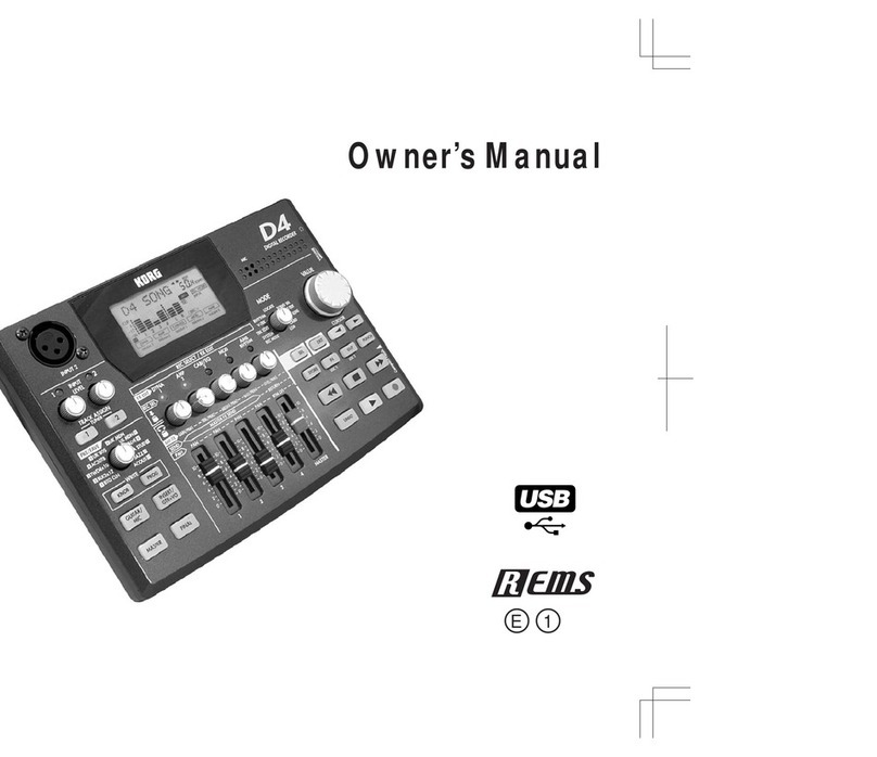
Yamaha D24 User manual

SERVICE MANUAL
PA 1/2
011458
HAMAMATSU, JAPAN
1.52K-8312 Printed in Japan '99.12
CONTENT
PROTECTION OF EYES
FROM LASER BEAM DURING SERVICING········ 3
SPECIFICATIONS···································································· 5
BLOCK DIAGRAM···································································· 6
CIRCUIT BOARD LAYOUT······················································ 9
PANEL LAYOUT····································································· 13
DISASSEMBLY PROCEDURE··············································· 15
LSI PIN DESCRIPTION·························································· 19
IC BLOCK DIAGRAM ····························································· 31
CIRCUIT BOARDS································································· 34
ERROR MESSAGES······························································ 38
SETTING THE SCSI······························································· 39
INITIALIZE·············································································· 40
CHECKING THE VERSION NUMBER··································· 40
UPDATING THE SYSTEM SOFTWARE································ 40
DIMENSIONS········································································· 40
EJECTING TROUBLESOME DISKS······································ 41
TEST PROGRAM··································································· 42
MIDI IMPLEMENTATION CHART·········································· 47
PARTS LIST
RC-D24 SERVICE MANUAL
OVERALL CIRCUIT DIAGRAM
D24: 19991210-380000
RC-D24: 19991210-48000
DIGITAL MULTITRACK RECORDER
REMOTE CONTROLLER/LOCATOR
D24

D24
2
WARNING: CHEMICAL CONTENT NOTICE!
The solder used in the production of this product contains LEAD. In addition, other electrical/electronic and/or plastic (where
applicable) components may also contain traces of chemicals found by the California Health and Welfare Agency (and possibly
other entities) to cause cancer and/or birth defects or other reproductive harm.
DO NOT PLACE SOLDER, ELECTRICAL/ELECTRONIC OR PLASTIC COMPONENTS IN YOUR MOUTH FOR ANY REASON
WHAT SO EVER!
Avoid prolonged, unprotected contact between solder and your skin! When soldering, do not inhale solder fumes or expose eyes
to solder/flux vapor!
If you come in contact with solder or components located inside the enclosure of this product, wash your hands before handling
food.
IMPORTANT NOTICE
This manual has been provided for the use of authorized Yamaha Retailers and their service personnel. It has been assumed that
basic service procedures inherent to the industry, and more specifically Yamaha Products, are already known and understood by
the users, and have therefore not been restated.
WARNING: Failure to follow appropriate service and safety procedures when servicing this product may result in personal
injury, destruction of expensive components and failure of the product to perform as specified. For these
reasons, we advise all Yamaha product owners that all service required should be performed by an authorized
Yamaha Retailer or the appointed service representative.
IMPORTANT: This presentation or sale of this manual to any individual or firm does not constitute authorization, certification,
recognition of any applicable technical capabilities, or establish a principal-agent relationship of any form.
The data provided is belived to be accurate and applicable to the unit(s) indicated on the cover. The research engineering, and
service departments of Yamaha are continually striving to improve Yamaha products. Modifications are, therefore, inevitable and
changes in specification are subject to change without notice or obligation to retrofit. Should any discrepancy appear to exist,
please contact the distributor's Service Division.
WARNING: Static discharges can destroy expensive components. Discharge any static electricity your body may have
accumulated by grounding yourself to the ground bus in the unit (heavy gauge black wires connect to this bus).
IMPORTANT: Turn the unit OFF during disassembly and parts replacement. Recheck all work before you apply power to the
unit.
WARNING
Components having special characteristics are marked and must be replaced with parts having specification equal to those
originally installed.
IMPORTANT NOTICE FOR THE UNITED KINGDOM
Connecting the Plug and Cord
IMPORTANT. The wires in this main lead are coloured in
accordance with the following code:
BLUE: NEUTRAL
BROWN: LIVE
As the colours of the wires in the main lead of this apparatus may not
correspond with the coloured markings identifying the terminals in
your plug, proceed as follows:
The BLUE wire must be connected to the terminal that is marked with
the letter N (or coloured BLACK).
The BROWN wire must be connected to the terminal that is marked
with the letter L (or coloured RED).
Be certain that neither core is connected to the earth terminal of the
three pin plug.

This set employs a laser. Therefore, be sure to carefully
follow the instructions below when servicing.
When checking the laser diode emission, keep your
eyes more than 30 cm away from the objective lens.
Laser Diode Properties
Material: AlGalnP
Wavelength: 675–695nm
Emission Duration: Continuous
Laser Output Power: Less than 44.6 µW
(Note) Laser output is measured at a distance of 20 cm
from the object lens on the optical pick-up head.
PROTECTION OF EYES FROM LASER BEAM DURING SERVICING
D24
3
WARNING Laser Safety
This product contains a laser beam component. This component may emit invisible, as well as
visible radiation, which may cause eye damage. To protect your eyes and skin from laser radiation,
the following precaution must be used during servicing of the unit.
1) When testing and / or repairing any component within the product, keep your eyes and skin more
than 30 cm away from the laser pick-up unit at all time. Do not stare the laser beam at any time.
2) Do not attempt readjustment, disassemble and repair of the laser pick-up, unless noted
elsewhere in this manual.
3) CAUTION - Use of controls or readjustments or performance of procedures other than those
specified herein may result in hazardous radiation exposure.

D24
4
• These labels are
located on the interior.
• Varningsanvisning för
laserstrålning. Placerad
i apparaten.
This label is located on the
exterior.
CLASS 1 LASER PRODUCT
LUOKAN 1 LASERLAITE
KLASS 1 LASERAPPARAT
Klassmärkning för Finland.
DANGER
DANGER
VORSICHT
ADVARSEL
VARNING
OSYNLIG LASERSTRÅLNING NÄR
DENNA DEL ÄR ÖPPEND. STRÅLEN
ÄR FARLIG.
APL
Recorder Unit
Bottom Cover

Recording medium 3.5" MO disk (ISO/ECMA) (Overwrite and
normal type)
Sound file format Yamaha proprietary format
Tracks
Main tracks 8
Virtual tracks 64 (8 per main track)
Simultaneous recording 8 tracks (44.1, 48 kHz), 4 tracks (88.2, 96 kHz)
Simultaneous playback 8
Sampling rate 44.1, 48 , 88.2 (Dual AES/EBU), 96 kHz (Dual
AES/EBU)
Recording resolution 16, 20, 24-bit
Maximum recording time
(44.1 kHz, 16-bit, 640 MB MO disks)
15 mins x8 tracks
30 mins x4 tracks
60 mins x2 tracks
120 mins x1 track
Shuttle playback 1/32 to 4x normal playback speed
Pitch control ±6 %
Repeat playback A–B Repeat
Punch in/out Auto, Manual, Rehearsal
Auto Punch multi-take recording Up to 99 takes
Locate
Project Select/Search
Locate point set/search LAST REC IN, LAST REC OUT, A, B
Locate memory
store/recall 99
Return to zero
Roll back
Editing
Undo/Redo, Copy, Insert Copy, Move, Erase, Delete,
Time Comp/Expand, Pitch Change, Optimize
Time Compression/Expansion 50 %–200 %
Pitch Change 50 %–200 % (±1,200 cents or ±1 octave)
Display
Type VFD (Vacuum Fluorescent Display)
Characters 12-character lines x2
Main counter Hours, minutes, seconds, frames
Counter mode ABS (Absolute), REL (Relative)
Track level meters 16 segment with OVER indicator x8
Analog Output
Digital Audio Input
Synchronization
Parallel unit chase (up to 8 units)
Serial unit chase (2 units)
External SMPTE/EBU timecode chase (24, 25,
30D, 30 fps)
External MTC chase
External MMC control
9-pin protocol control
Other
functions
Solo Select
Monitor Select Auto Input/All input
Peak Hold On/Off
Power requirements U.S.A. & Canada 120 V AC, 60 Hz
Europe 230 V AC, 50 Hz
Power consumption 100 W
Dimensions (W x H x D) 480 x 144 x 383.9 mm (18.9 x 5.7 x 15.1 inches)
Weight 13 kg (28.7 lbs)
Free-air operating temperature range
5 ˚C to 35 ˚C (41 ˚F to 95 ˚F)
Relative humidity 10 %–95 %
Accessories Power cord, MO disk, disk eject tool
Options Digital interface card (MY8, MY4 series)
RC-D24 Remote Controller
Connection
For Use With Nominal
Output Level Connector
PHONES*1
*1. 20-bit 8-times oversampling D/A converter.
40 phones 60 mW Stereo phone jack
(unbalanced)*2
*2. PHONES stereo phone jack is unbalanced (tip = left, ring = right, sleeve = ground).
Connection Format Wordlength Level Connector
COAXIAL
STEREO DIGITAL
INPUT
IEC-60958 16, 20, 24 bit 0.5 V pp
(75 ) Phono
Control I/O
Channel status
Type: 2 audio channels
Category code: 2 channel PCM encoder/decoder
Copy prohibit: No
Emphasis: No
Sampling rate: depends on internal configuration
Connection Format Level Connector
VIDEO INPUT Composite
(black burst or
color bar) — BNC
VIDEO OUTPUT Composite
(black burst or
color bar) — BNC
WORD CLOCK INPUT — TTL BNC
WORD CLOCK OUTPUT
— TTL BNC
MIDI IN MIDI — 5-pin DIN
MIDI OUT MIDI — 5-pin DIN
MIDI THRU MIDI — 5-pin DIN
SCSI Narrow SCSI-2
(FAST-20) — Half pitch 50-pin
SERIAL I/O 9-pin protocol RS-422 9-pin D-sub
SYNC OUT — RS-422 15-pin D-sub
REMOTE IN/SYNC IN — RS-422 15-pin D-sub
TIMECODE INPUT SMPTE/EBU — XLR-3-31 type (balanced)
TIMECODE OUTPUT SMPTE/EBU — XLR-3-32 type (balanced)
*1.
Connection Format Wordlength Level Connector
COAXIAL
STEREO DIGITAL
OUTPUT
IEC-60958*1
Consumer Use 16, 20, 24 bit 0.5 V pp
(75 ) Phono
Digital Audio Output
SPECIFICATIONS
D24
5

DPB
YM6029
DSPIII
DSPIII
YSS228
( 60MHz )
DUAL-PORT
SRAM 64K
CY7C024-15AC
4KW X 32bit
SCSI-2
CONTROLLER
( 1-4ch )
( 5-8ch )
GUI CPU
HD6477042AF28
( 16bit 28MHz)
FLASH ROM 4M
DRAM 16M
KM416C1200CJ-6T
( 1MW 16bit )
ACIA
YM6604C
TIME CODE
READER/
GENERATOR
ICS2008A
PIO
uPD71055
DS12887
MEDIA BAY
MEDIA CPU
HD6477043AF28
( 32bit 28MHz)
FLASH ROM
DRAM 64K
KM416C4100B-6
( 4MW 32bit )
YSS228
( 60MHz )
DSP
TMS320C32PCM60
( 60MHz )
( TIME COMP )
DUAL-PORT
SRAM 64K
CY7C136-25NC
( 2KW X 8bit )
SRAM 4M
CY7C1041-15VC
( 64kW X 32bit )
uPD72611GF-3BA
VFD
CONTROLLER
PANEL CPU
HD6417014F28
( 16bit 28MHz)
DRAM 16M
M6604FP
JOG/SHUTTLE
12:34:56
ABCDEFG
VFD
KEY SCAN
CONTROL
DUAL-PORT
SRAM CY7C024-15AC
4KW X 16bit
REMOCON/SYNC
MIDI
FLASH ROM 4M
FS GEN
&
OVER DET
3.5inch
MO DRIVE
SCSI BAS
EXT MEDIA
SCSI CONNECTOR
MBM29F400BC-70PF
(512KW 16bit)
GATE ARRAY
CRVPO8
REAL TIME
CLOCK
MBM29F400BC-70PF
(512KW 16bit)
MBM29F400BC-70PF
(512KW 16bit)
KM416C1200CJ-6T
( 1MW 16bit )
(RS-485)
RS-422
IC101
IC103 IC104
IC119
IC126 IC137 IC117
IC701
IC151 IC320
IC321 IC316
IC322
IC152
IC156IC118
IC301
IC302
IC303 IC308 IC318
IC309
IC157 IC703
CN703CN704
CN804CN802
IC801
IC704
IC138
IC139
CN101
CN702
IC128
IC217
MAIN-A
SUB
(BAY)
SUB
(PANEL)
FP
KEC-92354-1 1
BLOCK DIAGRAM
D24
6
CPU & SCI Section

BAY
I1
I2
I3
I4
O1
O2
O3
O4
SI1-1/2
SI1-3/4
SI1-5/6
SI1-7/8
SO1-1/2
SO1-3/4
SO1-5/6
SO1-7/8
7a
7b
9a
9b
3a
3b
5a
5b
CN711
IC138
CN712
CN713
CN714
IC143
CN503 CN111
CN715, 716, 717, 718
CN105, 104, 103, 102
IC144
JK12
JK12
7a
7b
9a
9b
3a
3b
5a
5b
7a
7b
9a
9b
3a
3b
5a
5b
7a
7b
9a
9b
3a
3b
5a
5b
SI2-1/2
SI2-3/4
SI2-5/6
SI2-7/8
SO2-1/2
SO2-3/4
SO2-5/6
SO2-7/8
SI3-1/2
SI3-3/4
SI3-5/6
SI3-7/8
SO3-1/2
SO3-3/4
SO3-5/6
SO3-7/8
SI4-1/2
SI4-3/4
SI4-5/6
SI4-7/8
SO4-1/2
SO4-3/4
SO4-5/6
SO4-7/8
SLOT1
SLOT2
SLOT3
SLOT4
I1
I2
I3
I4
O1
O2
O3
O4
I1
I2
I3
I4
O1
O2
O3
O4
I1
I2
I3
I4
O1
O2
O3
O4
SI1-1/2
SI1-3/4
SI1-5/6
SI1-7/8
SI2-1/2
SI2-3/4
SI2-5/6
SI2-7/8
SI3-1/2
SI3-3/4
SI3-5/6
SI3-7/8
SI4-1/2
SI4-3/4
SI4-5/6
SI4-7/8
13
12
11
10
9
8
71
2
3
4
53
52
59
60
61
63
64
65
51
52
56
61
62
63
12 11 IC152
50
49 IC151
6
54
55
56
58
59
61
62
63
DPB
YM6029
( INPUT SEL )
SO1-1/2
SO1-3/4
SO1-5/6
SO1-7/8
SO2-1/2
SO2-3/4
SO2-5/6
SO2-7/8
SO3-1/2
SO3-3/4
SO3-5/6
SO3-7/8
SO4-1/2
SO4-3/4
SO4-5/6
SO4-7/8
4
3
2
1
77
78
79
80
54
55
56
58
59
61
62
63
3
12
7
50 51
47 46
36
2
16
37
33 31 IC139
IC159
10
11
12
13
DPB
YM6029
( OUTPUT SEL )
SI-1/2
SI-3/4
SI-5/6
SI-7/8
SPDIN
66SPDOUT
SO-1/2
SO-3/4
SO-5/6
SO-7/8
DSPIII
DSPIII
YSS228
YSS228
32bit DSP DATA BUS
DUAL-PORT
SRAM 64K
32bit DATA BUS
4KW X 32bit
DRAM 64K
4MW X 32bit
SCSI-2
CONTROLLER
SCSI-2 BUS
640MB
MO DRIVER
DIR2
YM3436
DDIN DOUT
SI0
SI1
SI2
SI3
SI4
SI5
SI6
SI7
SB0
SB1
SB2
SB3
SB4
SB5
SB6
SB7
SO0
SO1
SO2
SO3
SO0
SO1
SO2
SO3
SO4
SO5
SO6
SO7
SB0
SB1
SB2
SB3
SB4
SB5
SB6
SB7
SI0
SI1
SI2
SI3
SI0
SI1
SI2
SI3
SI7
SO2
SO3
SO0
SO1
DA00
DA31
DA00
DA31
DA00
DA31
MD00
MD31
MD00
MD31
MD00
MD31
MD00
MD31
SB0
SB7
DIT2
YM3437
DIN
DOUT
IN
OUT
COAXIAL
FS
64FS
128FS
256FS
128FS 256FS SYNC
SYNC
128FS
SYNC
128FS
SO7
( 1-4ch )
( 5-8ch )
32bit DATA BUS
SO5
SO4
DR0
FSR0
DX0
IC320
TI DSP
TMS320C32PCM60
DR0
FSR1 1
3
7
6
DAC
48kHz
20bit 2ch
SDATA AOUTL
AOUTR
PHON-D
FS
64FS
256FS
PHONES
SPDIN
SPDOUT
SI3
DX0
DR0
DX0
SI4
FSX0
DUAL-PORT
SRAM 64K
4KW X 16bit
TD00
TD15
MD00
MD15
16bit DATA BUS
16bit DATA BUS
FSX1
FSR1
SO2
SO-1/2
SO-3/4
SI-5/6
SI-7/8
FSX1
SO4
SO7
SO-1/4
SO-5/8
SO-5/8
SO-1/4
EXT SCSI
CONNECTOR
FS GEN
&
OVER DET
GATE ARRAY
CRVPO8
CXDO
SYNC
128FS
CXSY
128CX
DSC4
YM6067
IC316
IC156
IC157
IC308
IC318
IC119
IC401
IC402
IC403
IC404
CN108
CN808
JK106
IC309
40
41
8
975
18 7
17 1
7
1
SUB(BAY) MAIN-A
MAIN-C
FP
KEC-92354-2 1
D24
7
AUDIO DATA IN/OUT Section

FS GEN
&
OVER DET
GATE ARRAY
CRVPO8 SYNC
FS
64FS
128FS
256FS
FS/8
FS/16
VCO_A
VCO_B
24.5760MHz
22.5792MHz
DIR2
YM3436
External
WC_Selector
WCKIN
WCKMY1
WCKMY2
SPDWCK
LINKFS
BAY
SPDIF
I/F
(
YM3436
)
DIR2
WORD CLOCK IN
OUT THRU
TERM
Mastor
/Slave
Switch
ICS2008A
Mastor
/Slave
Switch
Time_Code
Selector
(INT/EXT)
DATA
(
SELECTOR
)
Mastor
/Slave
Switch
TIME CODE
READER/
GENERATOR
LTC IN
VITC IN LRCK
LTC OUT
ON
OFF
75
VIDEO IN
OUT
XLINK FS
XLINK TC
TIME CODE
IN
OUT
REMOTE IN/
SYNC IN
SYNC OUT
128CX
CSSY
JK106
CN711
CN712
IC143
JK101
JK102
JK11
JK10 CN502 CN106
JK108
JK109
9
IC131
IC137
IC130
IC158
IC119
54
30
29
28
21
22
24
2638 32
8
IC125
IC123
IC120
XOC101
XOC102 42
46
10365
3
2
14
15
1
6
7
7
7
26
6
18
12, 13
3, 5 10, 11
38
9
JK107 DATA
(
SELECTOR
)
MAIN-B
MAIN-A
KEC-92354-3 1
D24
8
FS GEN. & TIME CODE Section

FP
CN109
CN110
Recoder unit
Front assembly
CN301
CN101
CN702
CN102
CN103
CN104
CN105
CN715
CN716
CN717
CN718
x4 CN108
CN111 CN106
CN10
CN11
CN12
CN13
CN1
CN2
FP
CN9
AC-IN connector
Power transformer
Fan
A
BC
1/2
Front assembly
CN719
CN4
CN6
CN8 CN7
CN3
CN5
CN701
CN808
E
F
D
G
H
K
I
JJ
CB
K
G
E
M
L
N
<Bottom View> <Top View>
MAIN-B
MAIN-A
MAIN-C
SUB(BAY)
SUB(PANEL) SUB(PANEL)
PS
2/2
PS
5/5
FP
4/5
FP
CIRCUIT BOARD LAYOUT
D24
9

D24
10
CN801
CN703
CN705
CN804
Sub chassis
CN807
CN806
CN805 CN708CN706CN707
CN808
Sub chassis
<Rear View>
<Front View> Right side
<Front View> Left side
CN704
CN802
Sub chassis
CN803
2/5
FP
2/5
FP
1/5
FP
1/5
FP
4/5
FP
3/5
FP
SUB(PANEL)
SUB(PANEL)
SUB(PANEL)
O
P
Q
H
T
S
R
K
AC-IN
MAIN A-CN106
MAIN A-CN111
FP5/5-CN9
PS2/2-CN5
PS2/2-CN4
PS2/2-CN3
FP2/5-CN803
PS2/2-CN7
PS2/2-CN6
FP4/5-CN808
MAIN A-CN301
MAIN A-CN102
MAIN A-CN103
MAIN A-CN104
MAIN A-CN105
MAIN A-CN101
FP2/5-CN804
FP1/5-CN801
FP1/5-CN802
FP3/5-CN807
FP3/5-CN805
FP3/5-CN806
PS1/2-CN10
MAIN B-CN502
MAIN C-CN503
PS1/2-CN11
Recorder Unit
SUB(BAY)-CN719
MAIN A-CN110
PS2/2-CN8
SUB(PANEL)-CN701
MAIN A-CN109
MAIN A-CN108
Recorder Unit
SUB(BAY)-CN718
SUB(BAY)-CN717
SUB(BAY)-CN716
SUB(BAY)-CN715
SUB(PANEL)-CN702
SUB(PANEL)-CN703
SUB(PANEL)-CN705
SUB(PANEL)-CN704
SUB(PANEL)-CN708
SUB(PANEL)-CN706
SUB(PANEL)-CN707
AC IN
KR
KR
PSW
MO
PH&PH
PS-MAIN
PH&PH
PH&PH
PH&PH
B&C
MAIN-MO
FFC
FFC
FFC
FFC
FFC
FFC
FFC
FFC
B&C
B&C
B&C
DESTINATION
CONNECTOR ASSEMBLY
3P/L230(BL,WH)
L190(GR)
6P/L160
5P/L160
3P/L300
4P/L250
12P/L500
6P-7P/L300
7P/L160
5P/L250
8P/L160
8P/L450
50P/L300
36P/L170
36P/L170
36P/L170
36P/L170
5P/L80
6P/L80
30P/L80
8P/L80
6P/L250
11P/L250
10P/L250
OVERALLASSEMBLY [300]
OVERALLASSEMBLY [560]
OVERALLASSEMBLY [570]
OVERALLASSEMBLY [500]
OVERALLASSEMBLY [550]
OVERALLASSEMBLY [520]
OVERALLASSEMBLY [510]
FRONT ASSEMBLY [330]
OVERALLASSEMBLY [540]
OVERALLASSEMBLY [530]
FP CIRCUIT BOARD [CN808]
OVERALLASSEMBLY [580]
OVERALLASSEMBLY [600]
OVERALLASSEMBLY [590]
FRONT ASSEMBLY [300]
FRONT ASSEMBLY [320]
FRONT ASSEMBLY [310]
FP CIRCUIT BOARD [CN807]
FP CIRCUIT BOARD [CN805]
FP CIRCUIT BOARD [CN806]
PIN/LENGHT PART LIST REF NO.
A
B
C
D
E
F
G
H
I
J
K
L
M
N
O
P
Q
R
S
T

W7
W8
W5W4W3W2
W6
Component side
S-SYNC
IC101
43pin
IC120
IC128
22pin
IC135
IC134
IC133
IC131
IC132
IC129IC136
IC130
8pin
6pin
IC317
CN-GL3
IC317
from W6
from W5
1
2
3
4
5
6
444342414039
1819202122
23242526
27
from W1
IC128 IC135IC134
from W2from W3
5
6
78
9
10
29 43
42
41 4445
28
IC101
RA101
RA102
RA103
from W8
from W7
IC120
W16
W15
W14
W13
2pin
12pin
2pin
5pin
from W15
from W16
IC136
IC132
Cut this pattern
Cut this pattern
1
2
3
4
5
6
7
1
2
3
4
5
6
7
14
13
12
11
10
9
8
IC129 from W13from W14
89pin
89pin
IC101
RA106
from W4
W4
Cut this pattern
D24
11
S-SYNC Circuit Board Wiring 1/2

50
1
78
14
RE BL
W13W14W15W16
W9
W10
W11
W12
Component side
IC158
IC125
7pin
14pin
VC101
35pin
36pin
CN-GL1
from W10 (BL)
from W9 (RE)
IC125
VC101
RE
8
IC119
3635 3433
32
31
30
373839
from W11
4951
52
53
54
Cut this pattern
R116
R117
R115
R118 C141
C151
C142 R119
R120
Remove the parts
R118
C151
MAIN-A Circuit Board revision
Jumper wire
to MAIN-R120
to S-SYNC-W12
C143
R121
C144
C145 L116
15p 47p
(Change)
BL
CN-GL1
CN-GL3
(VG85200)
Spacer
Spacer
(VG85200)
S-SYNC Circuit Board instllation
S-SYNC
MAIN-A
S-SYNC
MAIN-A
D24
12
S-SYNC Circuit Board Wiring 2/2

PANEL LAYOUT
D24
13
00 00 00 00
OVER
READY
0
2
6
10 12
14 20
18 30
20 42
26 60
–dB OVER ABS H
LOCK
TIME DISPLAY
CAPTURE ABS/REL REMAIN
VARI
SPEED UTILITY SETUP
PROJECT
SELECT
LOC MEM
RECALL
LOC MEM
STORE
LOCATEENTERCANCEL
0/-
1
4
7
8
R
7654321
RECORD
READY
SOLO/
SELECT
MONITOR SELECT
PEAK
HOLD AUTO
INPUT ALL
INPUT FORMAT CHASE
L
2
5
8
3
6
9
UNDO/
REDO
EDIT
JOG ON
JOG/DATA SHUTTLE/
CURSOR
PROJECT SEARCH
RTN TO
ZERO
REW FF STOP PLAY REC
ROLL
BACK
LAST REC SET
DIGITAL MULTITRACK RECORDER
REPEAT REHE
PHONES
LEVEL
010
ON
POWER
OFF
PHONES
BA
B
A
AUTO
PUNCH
IN OUT
INT 24 48K
MASTER
WC
BIT FS
TC
MSF
READY
0
2
6
12
20
30
42
60
–dB
V. TR AC K
SELECT
00 00 00 00
OVER
READY 12345678
0
2
6
10 12
14 20
18 30
20 42
26 60
–dB OVER ABS
REL H
LOCK
R
L
INT EXT
16 20 24 44.1K48K96KVARI
MASTER SLAVE
WC
BIT FS
TC
CHASE
MS F
READY
0
2
6
12
20
30
42
60
–dB
000000000000
000000000000
5467890q
321
Display
w
e
rty u
i
omnb¡
™ £ • ª
§ ¶
º œ ∞ ∑ ¢ ´ ®
¨
¥
pag
f
d
s
kzv
j;c
hlx
†/.,
231
3
12
REMOTE IN/
SYNC IN
SYNC OUT
SLOT 1 (ANALOG IN)
TIME CODE
MODEL D24
DIGITAL MULTITRACK RECORDER
OUTPUT INPUT
OUTPUT INPUT
COAXIAL
STEREO DIGITAL
AC IN
VIDEO
OUTPUT OUTPUT
INPUT WORD CLOCK THRU OUT IN
MIDI
INPUT
75
ON OFF
SERIAL I/OSCSI
75
TERM THRU
SLOT 2 (ANALOG IN)
SLOT 3 (ANALOG OUT)
SLOT 4 (ANALOG OUT)
ˆ ø π å ß ∂ ƒ © ˙ ∆ ˚
¬ … Ω ≈ ç √ ∫
Level meters
Display Section
1
ABS/REL indicators
2
RECORD READY buttons 1-8
Track Buttons Section
w
SOLO/SELECT buttons & indicators 1-8
e
Counter
3
READY indicators
4
Message area
5
PEAK HOLD button & indicator
Peak, Monitor, Format & Chase Buttons Section
r
AUTO INPUT button & indicator
t
ALL INPUT button & indicator
y
FORMAT button & indicator
u
CHASE button & indicator
i
LOCK indicator
6
CHASE indicator
7
Keypad buttons
Keypad Section
o
CANCEL button
p
ENTER button
a
PROJECT SELECT button & indicator
s
LOC MEM RECALL button & indicator
d
LOC MEM STORE button & indicator
f
LOCATE button
g
WC window
8
BIT window
9
FS window
0
TC window
q
Front Panel Displayl
Rear panel

D24
14
CAPTURE button
Function Buttons Section
hVARI SPEED button & indicator
jV. TRACK SELECT button & indicator
k
POWER switch
Power Switch & Phones Section
† PHONES LEVEL control
¥ PHONES jack
¨
JOG ON button & indicator
Jog/Data & Shuttle/Cursor Controls Section
bJOG/DATA dial
nSHUTTLE CURSOR ring
m
ABS/REL button
lUTILITY button & indicator
;EDIT button & indicator
zREMAIN button & indicator
xSETUP button & indicator
cUNDO/REDO button & indicator
v
MO disk drive slot
Transport Controls Section
,Manual eject hole
.Eject button & activity indicator
/PROJECT SEARCH buttons
¡ RTN TO ZERO button
™ ROLL BACK button
£ LAST REC IN & OUT buttons & indicators
¢ A & B buttons & indicators
∞ SET button
§ AUTO PUNCH button & indicator
¶ REPEAT button & indicator
• REHE button & indicator
ª REW button
º FF button
œ STOP button
∑ PLAY button
´ REC button
®
VIDEO OUTPUT connector
Rear Panel
ˆ VIDEO INPUT connector
ø VIDEO 75 ON/OFF switch
π WORD CLOCK 75 TERM/THRU switch
å WORD CLOCK OUTPUT connector
ß WORD CLOCK INPUT connector
∂ MIDI IN, OUT & THRU ports
ƒ SCSI port
© SERIAL I/O port
˙ SYNC OUT port
∆ REMOTE IN/SYNC IN port
˚ Cooling fan
¬ AC IN connector
… TIMECODE OUTPUT connector
Ω TIMECODE INPUT connector
≈ COAXIAL STEREO DIGITAL OUTPUT connector
ç COAXIAL STEREO DIGITAL INPUT connector
√ SLOTs 1-4
∫

<Top View>
(Fig. 3) (Fig. 4)
[400]
[400] [400]
[350]
[160]
[160] [680]
[200A]
[200A]
[400]: Bind Head Tapping Screw-B 3.0X8 MFZN2BL (EP600190)
[160]: Pan Head Screw SP4.0X25 MFZN2BL (VR116500)
[200A]: Bind Head Tapping Screw-B 3.0X8 MFZN2BL (VP157000)
[350]: Bind Head Screw A3.0X12 MFZN2BL (VP156600)
[370]: Screw (VT362500)
[380]: Pan Head Screw 2.6X6 MFNI33 (VT267800)
[390]: Bind Head Tapping Screw-B 3.0X8 MFZN2BL (VP157000)
[680]: Bind Head Screw 4.0X12 MFZN2BL (VP156900)
MAIN-A MAIN-B MAIN-C
S-SYNC
[390] [380] [370]
Fan
3. MAIN-A and S-SYNC Circuit Boards
3-1 Remove the top cover. (See procedure 1.)
3-2 Remove the six (6) screws marked [400]. (Fig.3)
3-3 The four (4) screws marked [350], the two (2) screws
marked [390], the two (2) screws marked [380] and the six
(6) screws marked [370]. The MAIN-A circuit board and
the S-SYNC circuit board can then be removed. (Fig.4)
<Top View> <Bottom View>
Top cover
(Fig. 1) (Fig. 2)
[660]
[480]
[480]
[660]: Bind Head Tapping Screw-B 4.0X8 MFZN2BL (VC688800) [480]: Bind Head Tapping Screw-B 4.0X8 MFZN2BL (VC688800)
Bottom assembly
1. Top Cover
1-1 Remove the eleven (11) screws marked [660]. The top
cover can then be removed. (Fig.1)
2. Bottom Assembly
2-1 Remove the eleven (11) screws marked [480]. The bottom
assembly can then be removed. (Fig.2)
D24
15
DISASSEMBLY PROCEDURE

<Top View> • Power Supply Assembly
(Fig. 5) (Fig. 6)
[250A]
[250A]
[10c] [270]
[60A]
[60A]
[80]
[100]
[10c]: Bind Head Tapping Screw-B 4.0X8 MFZN2BL (VC688800)
[250A]: Bind Head Tapping Screw-B 3.0X8 MFZN2BL (EP600190)
[270]: Bind Head Tapping Screw-B 4.0X12 MFZN2BL (VD831800)
[60A]: Bind Head Tapping Screw-B 3.0X8 MFZN2BL (EP600190)
[80]: Bind Head Tapping Screw-B 3.0X8 MFZN2BL (VP157000)
[100]: Bind Head Tapping Screw-B 3.0X8 MFZN2BL (VP157000)
PS 1/2
PS 2/2
Power
transformer
Power supply assembly
TR holder (A)
TR holder (B)
D24
16
4. MAIN-B and MAIN-C Circuit Boards, Fan,
Power Transformer, PS1/2 and PS2/2
Circuit Boards
4-1 Remove the bottom assembly. (See procedure 2.)
4-2 MAIN-B Circuit Board: Remove the four (4) screws
marked [200A]. The MAIN-B circuit board can then be
removed. (Fig.4)
4-3 MAIN-C Circuit Board: Remove the two (2) screws
marked [680]. The MAIN-C circuit board can then be
removed. (Fig.4)
4-4 Fan: Remove the four (4) screws marked [160]. The fan
can then be removed. (Fig.4)
4-5 Power Transformer: Remove the four (4) screws marked
[10c]. The power transformer can then be removed. (Fig.5)
4-6 PS1/2 Circuit Board: Remove the four (4) screws marked
[250A]. The PS1/2 circuit board can then be removed.
(Fig.5)
4-7 PS2/2 Circuit Board: Remove the two (2) screws marked
[270]. The power supply assembly can then be removed.
(Fig.5)
Remove the three (3) screws marked [80] and the two (2)
screws marked [100]. The TR holder (A) and (B) can then
be removed. (Fig.6)
Remove the five (5) screws marked [60A]. The PS2/2
circuit board can then be removed. (Fig.6)

D24
17
5. SUB(BAY) Circuit Board
5-1 Remove the bottom assembly. (See procedure 2.)
5-2 Remove the power supply assembly. (See procedure 4-7.)
5-3 Remove the five (5) screws marked [440]. The front
assembly can then be removed. (Fig.7)
5-4 Remove the eight (8) screws marked [50]. The SUB(BAY)
circuit board can then be removed. (Fig.7)
6. FP1/5, FP2/5, FP3/5, FP4/5, FP5/5 and
SUB(PANEL) Circuit Boards
6-1 Remove the top cover. (See procedure 1.)
6-2 Remove the bottom assembly. (See procedure 2.)
6-3 Remove the front assembly. (See procedure 5-3.)
6-4 FP1/5 Circuit Board: Remove the two (2) screws marked
[250B]. The front panel can then be removed. (Fig.8)
Remove the three (3) screws marked [140]. The FP1/5
circuit board can then be removed. (Fig.8)
6-5 FP2/5 Circuit Board: Remove the front panel and the
FP1/5 circuit board. (See procedure 6-4.)
Remove the three (3) screws marked [120]. The FP2/5
circuit board can then be removed. (Fig.8)
6-6 FP3/5 Circuit Board: Remove the front panel. (See
procedure 6-4.)
Remove the four (4) screws marked [180]. The sub panel
can then be removed. (Fig.8)
Remove the four (4) screws marked [170]. The FP3/5
circuit board can then be removed. (Fig.8)
6-7 FP4/5 Circuit Board: Remove the front panel. (See
procedure 6-4.)
Remove the knob, and remove the two (2) nuts marked
[70]. The FP4/5 circuit board can then be removed. (Fig.8)
Bottom Side
Top Side
Front assembly
(Fig. 7)
[440]
[440]
[50]: Bind Head Tapping Screw-B 3.0X8 MFZN2BL (EP600190)
[440]: Bind Head Tapping Screw-B 4.0X8 MFZN2BL (VC688800)
[440]
[50]
[440]
[50]
SUB(BAY)

<Top View>
(Fig. 9) (Fig. 10)
[10f]
[10g]
[10g]: Bind Head Tapping Screw-B A3.0X8 MFZN2BL (VP157000) [10f]: Bind Head Screw A3.0X6 MFZN2BL (VP156600)
Recorder unit
Recorder unit
Angle
[10f]
Angle
7. Recorder Unit
7-1 Remove the top cover. (See procedure 1.)
7-2 Remove the four (4) screws marked [10g]. The recorder
unit can then be removed by sliding backward. (Fig.9)
7-3 Remove the four (4) screws marked [10f]. The two angles
can then be removed. (Fig.10)
(Fig. 8)
[120]
[120]
[140]
[60B]: Bind Head Screw 3.0X12 MFZN2BL (VP156600)
[120]: Bind Head Tapping Screw-B 3.0X8 MFZN2BL (EP600190)
[140]: Bind Head Tapping Screw-B 3.0X8 MFZN2BL (EP600190)
[170]: Bind Head Tapping Screw-B 3.0X8 MFZN2BL (EP600190)
[180]: Bind Head Tapping Screw-B 3.0X8 MFZN2BL (EP600190)
[200B]: Bind Head Tapping Screw-B 3.0X8 MFZN2BL (EP600190)
[250B]: Bind Head Tapping Screw-B 4.0X8 MFZN2BL (VC688800)
FP 2/5
FP 1/5
FP 3/5
FP 4/5
FP 5/5
SUB(PANEL)
Front panel
Sub panel Knob
Power swith knob
[140]
[250B]
[180]
[180] [70]
[60B]
[170]
[200B]
[250B]
D24
18
6-8 FP5/5 Circuit Board: Remove the front panel. (See
procedure 6-4.)
Remove the power switch knob, and remove the two (2)
screws marked [60B]. The FP5/5 circuit board can then be
removed. (Fig.8)
6-9 SUB(PANEL) Circuit Board: Remove the two (2) screws
marked [200B]. The SUB(PANEL) circuit board can then
be removed. (Fig.8)

PIN
NO. I/O FUNCTIONNAME PIN
NO. I/O FUNCTIONNAME
1
2
3
4
5
6
7
8
9
10
11
12
13
14
15
16
17
18
19
20
21
22
23
24
25
26
27
28
29
30
31
32
DIG11
DIG10
DIG09
DIG08
DIG07
DIG06
DIG05
DIG04
DIG03
DIG02
DIG01
DIG00
/RESET
/CS
SCK
SDATA
P1
P0
VCC1
XOUT
XIN
VSS
SEG35
SEG34
SEG33
SEG32
SEG31
SEG30
SEG29
SEG28
SEG27
VP
O
O
O
O
O
O
O
O
O
O
O
O
I
I
I
I
O
O
-
O
I
-
O
O
O
O
O
O
O
O
O
-
Digital output
Reset
Chip selection
Sift clock
Serial data
Output port 1
Output port 0
Power supply
Clock out
Clock in
Ground
Segment output
(-) Power supply
33
34
35
36
37
38
39
40
41
42
43
44
45
46
47
48
49
50
51
52
53
54
55
56
57
58
59
60
61
62
63
64
SEG26
SEG25
SEG24
SEG23
SEG22
SEG21
SEG20
SEG19
SEG18
SEG17
SEG16
SEG15
SEG14
SEG13
SEG12
SEG11
SEG10
SEG09
SEG08
SEG07
SEG06
SEG05
SEG04
SEG03
SEG02
SEG01
SEG00
VCC2
DIG15
DIG14
DIG13
DIG12
O
O
O
O
O
O
O
O
O
O
O
O
O
O
O
O
O
O
O
O
O
O
O
O
O
O
O
O
O
O
O
Segment output
Power Supply
Digital output
M66004FP (XT828A00) Display Driver FP: IC801
D24
19
LSI PIN DESCRIPTION
M66004FP (XT828A00) Display Driver····················································································· 19
HD6417014F28 (XU147A00) • EHD6477042AF28 (XV731A00) CPU ····································· 20
HD6477043AF28 (XV736A00) CPU ························································································· 21
TMS320C32PCM60 (XU277A00) DSP ···················································································· 22
YM6067 (XH494A00) PSC4 ····································································································· 23
YM6604 (XH497A00) ACIA ······································································································ 24
YSS228D-F (XQ962D00) DSP3 ······························································································· 25
µPD72611GF-3BA (XU375A00) SCSI Controler ······································································ 26
AK4321 (XS388A00) DAC ········································································································ 27
CRVP08 (XV740A00) Gate Array ····························································································· 27
DS12887 (XV618A00) Real Time Clock ··················································································· 28
ICS2008A (XV619A00) T.C. Reader/Generator ······································································· 28
YM3437C-F (XM530A00) DIT2 ································································································ 29
YM6029 (XH746A00) DPB ······································································································· 29
YM3436DK (XG948E0) DIR2 ··································································································· 30
µPD71055GB-3B4 (XH600A00) PIO ························································································ 30

D24
20
PIN
NO. I/O FUNCTIONNAME PIN
NO. I/O FUNCTIONNAME
1
2
3
4
5
6
7
8
9
10
11
12
13
14
15
16
17
18
19
20
21
22
23
24
25
26
27
28
29
30
31
32
33
34
35
36
37
38
39
40
41
42
43
44
45
46
47
48
49
50
51
52
53
54
55
56
PE14
PE15
VSS
A0
A1
A2
A3
A4
A5
A6
A7
A8
A9
A10
A11
A12
A13
A14
A15
A16
VCC
A17
VSS
/RAS
/CASL
/CASH
VSS
RDWR / PB5
A18
A19
A20
PB9 /A21
VSS
/RD
/WDTOVF
/WRH
VCC
/WRL
VSS
/CS1
/CS0
PA9 / TCLKD
/IRQ2 / TCLKC
/CS3
/CS2
/IRQ1
TXD
RXD
/IRQ0
PA1 / TXD0
PA0 / RXD0
D15
D14
D13
VSS
D12
O
O
I
O
O
O
O
O
O
O
O
O
O
O
O
O
O
O
O
O
I
O
I
O
O
O
O
O
O
O
O
O
I
O
O
O
I
O
I
O
O
O
I
O
O
I
O
I
I
O
I
I/O
I/O
I/O
I
I/O
Port E
Port E
Ground
Address bus
Power supply
Address bus
Ground
Row address strobe
Column address strobe (low)
Column address strobe (high)
Ground
DRAM read/write / Port B
Address bus
Port B / Address bus
Ground
Read
Watch dog timer overflow
High write
Power supply
Low write
Ground
Chip select
Chip select
Port A / Timer clock
Interrupt request / Timer clock
Chip select
Chip select
Interrupt request
Data transmission
Data reception
Interrupt request
Port A / Data transmission
Port A / Data reception
Data bus
Ground
Data bus
57
58
59
60
61
62
63
64
65
66
67
68
69
70
71
72
73
74
75
76
77
78
79
80
81
82
83
84
85
86
87
88
89
90
91
92
93
94
95
96
97
98
99
100
101
102
103
104
105
106
107
108
109
110
111
112
D11
D10
D9
D8
VSS
D7
D6
D5
VCC
D4
D3
D2
D1
D0
VSS
XTAL
MD3
EXTAL
MD2
NMI
VCC
MD1
MD0
PLLVCC
PLLCAP
PLLVSS
PA15 / CK
/RES
PE0
PE1
PE2
PE3
PE4
VSS
AN0 / PF0
AN1 / PF1
AN2 / PF2
AN3 / PF3
AN4 / PF4
AN5 / PF5
AVSS
AN6 / PF6
AN7 / PF7
AVCC
VSS
PE5
VCC
PE6
PE7
PE8
PE9
PE10
VSS
PE11
PE12
PE13
I/O
I/O
I/O
I/O
I
I/O
I/O
I/O
I
I/O
I/O
I/O
I/O
I/O
I
I
I
I
I
I
I
I
I
I
I
I
O
I
I
I
I
I
I
I
I
I
I
I
I
I
I
I
I
I
I
O
I
O
O
O
O
O
I
O
O
O
Data bus
Ground
Data bus
Power supply
Data bus
Ground
Crystal oscillator
Mode control
Crystal oscillator
Mode control
Non-maskable interrupt request
Power supply
Mode control
Mode control
PLL Power supply
PLL capacitor
PLL Ground
Port A / Clock
Reset
Port E
Ground
Analog input / Port F
Analog ground
Analog input / Port F
Power supply
Ground
Port E
Power supply
Port E
Ground
Port E
HD6417014F28 (XU147A00) CPU
HD6477042AF28 (XV731A00) CPU SUB(BAY): IC701
IC101MAIN:
Other manuals for D24
2
This manual suits for next models
1
Table of contents
Other Yamaha Voice Recorder manuals

Yamaha
Yamaha POCKETRAK CX User manual

Yamaha
Yamaha POCKETRAK 2G - 2 GB Digital Player User manual

Yamaha
Yamaha POCKETRAK C24 User manual

Yamaha
Yamaha Pocketrack C24 Quick start guide

Yamaha
Yamaha PocketrakCX - POCKETRAK CX 2 GB Digital... User manual

Yamaha
Yamaha YRM-301 User manual

Yamaha
Yamaha POCKETRAK C24 User manual

Yamaha
Yamaha POCKETRAK W24 User manual

Yamaha
Yamaha Tenor User manual

Yamaha
Yamaha POCKETRAK 2G - 2 GB Digital Player User manual