York MILLENIUM 351-46 User manual

OPERATING INSTRUCTIONS
MILLENNIUM
VARIABLE SPEED DRIVE
Supersedes: 160.00-O1 (702) Form 160.00-O1 (1020)
This Instruction is to be used in conjunction with the standard
Operating Instructions for YORK Model YT & YK chillers
furnished with an optional Variable Speed Drive (VSD).
TABLE OF CONTENTS
VSD Style Variations .......................................................................................... 2
VSD Unit and Harmonic Filter Component Overview......................................... 2
VSD Control System Overview........................................................................... 7
Control Panel VSD Related Keypad Functions ................................................ 10
VSD Adaptive Capacity Control........................................................................ 12
VSD Display Messages.................................................................................... 13
YORK MODEL YK CHILLER WITH OPTIONAL VARIABLE SPEED DRIVE
VSD SIZE (HP)
60 HZ 50 HZ
351 292
503 419
790 658
1100 900

JOHNSON CONTROLS
2
FORM 160.00-O1 (1020)
This equipment is a relatively complicated apparatus.
During rigging, installation, operation, maintenance,
or service, individuals may be exposed to certain com-
ponents or conditions including, but not limited to:
heavy objects, refrigerants, materials under pressure,
rotating components, and both high and low voltage.
Each of these items has the potential, if misused or
handled improperly, to cause bodily injury or death. It
is the obligation and responsibility of rigging, instal-
lation, and operating/service personnel to identify and
recognize these inherent hazards, protect themselves,
and proceed safely in completing their tasks. Failure
to comply with any of these requirements could result
in serious damage to the equipment and the property in
IMPORTANT!
READ BEFORE PROCEEDING!
GENERAL SAFETY GUIDELINES
which it is situated, as well as severe personal injury or
death to themselves and people at the site.
This document is intended for use by owner-authorized
rigging, installation, and operating/service personnel. It
is expected that these individuals possess independent
training that will enable them to perform their assigned
tasks properly and safely. It is essential that, prior to
performing any task on this equipment, this individual
shall have read and understood the on-product labels,
this document and any referenced materials. This in-
dividual shall also be familiar with and comply with
all applicable industry and governmental standards and
regulations pertaining to the task in question.
SAFETY SYMBOLS
The following symbols are used in this document to alert the reader to specific situations:
Indicates a possible hazardous situation
which will result in death or serious injury
if proper care is not taken.
Indicates a potentially hazardous situa-
tion which will result in possible injuries
or damage to equipment if proper care is
not taken.
Identifies a hazard which could lead
to damage to the machine, damage to
other equipment and/or environmental
pollution if proper care is not taken or
instructions and are not followed.
Highlights additional information useful
to the technician in completing the work
being performed properly.
External wiring, unless specied as an optional connection in the manufacturer’s product line, is not
to be connected inside the control cabinet. Devices such as relays, switches, transducers and controls
and any external wiring must not be installed inside the micro panel. All wiring must be in accor-
dance with Johnson Controls’ published specications and must be performed only by a qualied
electrician. Johnson Controls will NOT be responsible for damage/problems resulting from improper
connections to the controls or application of improper control signals. Failure to follow this warning
will void the manufacturer’s warranty and cause serious damage to property or personal injury.

FORM 160.00-O1 (1020)
JOHNSON CONTROLS 3
CHANGEABILITY OF THIS DOCUMENT
In complying with Johnson Controls’ policy for contin-
uous product improvement, the information contained
in this document is subject to change without notice.
Johnson Controls makes no commitment to update
or provide current information automatically to the
manual or product owner. Updated manuals, if appli-
cable, can be obtained by contacting the nearest John-
son Controls Service office or accessing the Johnson
Controls Knowledge Exchange website at https://docs.
johnsoncontrols.com/chillers/.
It is the responsibility of rigging, lifting, and operating/
service personnel to verify the applicability of these
documents to the equipment. If there is any question
regarding the applicability of these documents, rig-
ging, lifting, and operating/service personnel should
verify whether the equipment has been modified and
if current literature is available from the owner of the
equipment prior to performing any work on the chiller.
REVISION NOTES
Revisions made to this document are indicated in the following table. These revisions are to technical information,
and any other changes in spelling, grammar, or formatting are not included.
AFFECTED PAGES DESCRIPTION
3 Conditioned Based Maintenance program information added
CONDITIONED BASED MAINTENANCE
Traditional chiller maintenance is based upon assumed
and generalized conditions. In lieu of the tradition-
al maintenance program, a Johnson Controls YORK
Conditioned Based Maintenance (CBM) program can
be substituted. This CBM service plan is built around
the specific needs for the chiller, operating conditions,
and annualized impact realized by the chiller. Your lo-
cal Johnson Controls Branch can propose a customized
Planned Service Agreement that leverages real time
and historical data, delivering performance reporting,
corrective actions required and data enabled guidance
for optimal operation and lifecycle assurance. The pro-
gram will include fault detection diagnostics, operation
code statistics, performance based algorithms and ad-
vance rules based rationale delivered by the Johnson
Controls Connected Equipment Portal.

JOHNSON CONTROLS
4
FORM 160.00-O1 (1020)
VSD STYLE VARIATIONS
Original Style –
Model Number Part Number
351 -46 371-01742-XXX
503 -46 371-01484-XXX
790 -46 371-01749-XXX
Style “A” – This series applies to 503 HP only. Ground
fault protection was incorporated into the circuit breaker,
rather than utilizing separate GFI modules.
Model Number Part Number
503 - 46A 371-02241-XXX
Style “B” – This series includes wire harness changes
to address 50HZ, higher voltage scaling on the ‘519’
Filter Logic Board with matching software changes,
and various other software modications. Note: Style
“B” Software cannot be installed in Style A units without
also making signicant hardware changes.
Model Number Part Number
351 - 46B 371-02289-XXX
503 - 46B 371-02291-XXX
790 - 46B 371-02293-XXX
292 - 50B (50 HZ) 371-02249-XXX
419 - 50B (50 HZ) 371-02248-XXX
658 - 50B (50 HZ) 371-02247-XXX
Style “C” – This series is identical to the Style B series,
except that the circuit breaker and some fuses have been
changed to permit a 65,000 A. Short-Circuit Rating.
Model Number Part Number
351 - 46C 371-02412-XXX
503 - 46C 371-02413-XXX
790 - 46C 371-02414-XXX
292 - 50C (50 HZ) 371-02415-XXX
419 - 50C (50 HZ) 371-02416-XXX
658 - 50C (50 HZ) 371-02417-XXX
Style “D” – This series incorporates changes to the
‘519’ Filter Logic Board and Filter Gate Driver Board,
resulting in improved Percent TDD values:
Model Number Part Number
351 -46D 371-02526-XXX
503 -46D 371-02527-XXX
790 -46D 371-02528-XXX
1100 -46D 371-02461-XXX
292 -50D 371-02529-XXX
419 -50D 371-02530-XXX
658 -50D 371-02531-XXX
900 -50D 371-02532-XXX
- XXX Sux:
-101 Factory Package YT Basic
-102 Factory Package YK Basic
-103 Factory Package YT w/ Filter
-104 Factory Package YK w/ Filter
-111 Retrot YT Basic
-112 Retrot YK Basic
-113 Retrot YT w/ Filter
-114 Retrot YK w/ Filter
VSD UNIT AND HARMONIC FILTER
COMPONENT OVERVIEW
Variable Speed Drive
The new YORK VSD is a liquid cooled, transistorized,
PWM inverter packaged in a compact cabinet small
enough to mount directly onto the chiller and directly onto
the motor. The power section of the drive is composed of
four major blocks: an AC to DC rectier section with ac-
companying pre-charge circuit and free-wheeling diode,
a DC link lter section, a three phase DC to AC inverter
section and an output suppression network.
The AC to DC rectifier utilizes a semi-converter
formed by the connection of three SCR/diode modules
(1SCR-3SCR) in a three phase bridge conguration
(See Fig. 1). The modules are mounted on a liquid
cooled heatsink. Use of the semi-converter congura-
tion permits implementation of a separate pre-charge
circuit to limit the ow of current into the DC link lter
capacitors when the drive is switched on and it also
provides a fast disconnect from the power mains when
the drive is switched o. When the drive is turned o,
the SCRs in the semi-converter remain in a non-con-
ducting mode and the DC link lter capacitors remain
uncharged. When the drive is commanded to run, a set
of precharge resistors (1RES, 2RES) are switched into
the circuit by contactor 1M. The DC link lter capacitors
are slowly charged via the precharge resistors and the
diodes of the semi-converter for a xed time period of 15
seconds. After the 15 second time period has expired,
the SCR’s are gated fully on and the contactor 1M is
dropped out. A “free-wheeling” diode 1CR is included
to reduce the surge current which must be conducted
through the semi-converter if a serious fault were to oc-
cur across the DC link. Three power fuses (1FU - 3FU)
and an electronic circuit breaker (1SW) with ground fault
sensing connects the AC to DC converter to the power
mains. Very fast semiconductor power fuses are utilized
to ensure that the SCR/diode module packages do not
rupture if a catastrophic failure were to occur on the DC
link. The SCR Trigger board (031-01472) provides the
gating pulses for the SCR’s as commanded by the VSD
Logic board (031-01433).
The DC Link lter section of the drive consists of two
basic components, a DC Link “smoothing” inductor or
pair of inductors (1L, 2L) and a series of electrolytic
lter capacitors (C1-C36). This inductor / capacitor
combination forms a low-pass L-C lter which eectively
smooths the ripple voltage from the AC to DC rectier
while simultaneously providing a large energy reservoir
for use by the DC to AC inverter section of the drive.
In order to achieve a suitable voltage capability for the
capacitor portion of the lter, lter capacitor “banks” are
formed by connecting two capacitors in series to form a
“pair”, and then paralleling a suitable number of “pairs”

FORM 160.00-O1 (1020)
JOHNSON CONTROLS 5
THIS PAGE INTENTIONALLY LEFT BLANK.

JOHNSON CONTROLS
6
FORM 160.00-O1 (1020)

FORM 160.00-O1 (1020)
JOHNSON CONTROLS 7

JOHNSON CONTROLS
8
FORM 160.00-O1 (1020)
to form a capacitor “bank”. In order to assure an equal sharing
of the voltage between the series connected capacitors and
to provide a discharge means for the capacitor bank when the
VSD is powered o, “bleeder” resistors (3RES and 4RES) are
connected across the capacitor banks.
The DC to AC inverter section of the VSD (See Fig. 2), serves
to convert the rectied and ltered DC back to AC at the mag-
nitude and frequency commanded by the VSD Logic board.
The inverter section is actually composed of three identical
inverter output phase assemblies. These assemblies are in
turn composed of a series of Insulated Gate Bipolar Transistor
(IGBT) modules (Q1-Q4) mounted to a liquid cooled heatsink, a
lter capacitor “bank” (C13-C20) and a VSD Gate Driver board
(031-01476) which provides the On and O gating pulses to
the IGBT’s as determined by the VSD Logic board. In order
to minimize the parasitic inductance between the IGBT’s and
the capacitor banks, copper plates which electrically connect
the capacitors to one another and to the IGBT’s are connected
together using a “laminated bus” structure. This “laminated
bus” structure is a actually composed of a pair of copper bus
plates with a thin sheet of insulating material acting as the
separator/insulator. The “laminated bus” structure forms a
parasitic capacitor which acts as a small valued capacitor,
eectively canceling the parasitic inductance of the busbars
themselves. To further cancel the parasitic inductances, a se-
ries of small lm capacitors (C43-C51) are connected between
the positive and negative plates of the DC link. To provide
electrical shielding for the VSD Gate Driver board, an IGBT
driver “shield board” (031-01627) is mounted just beneath the
VSD Gate Driver board.
The VSD output suppression network is composed of a
series of capacitors (C61-C66) and resistors (5RES-10RES)
connected in a three phase delta conguration. The param-
eters of the suppression network components are chosen
to work in unison with the parasitic inductance of the DC to
AC inverter sections in order to simultaneously limit both the
rate of change of voltage and the peak voltage applied to
the motor windings. By limiting the peak voltage to the motor
windings, as well as the rate-of-change of motor voltage, we
can avoid problems commonly associated with PWM motor
drives, such as stator-winding end-turn failures and electrical
uting of motor bearings.
Various ancillary sensors and boards are used to convey
information back to the VSD Logic board. Each liquid cooled
heatsink within the DC to AC inverter section contains a
thermistor heatsink temperature sensor (RT1 - RT3) to provide
temperature information to the VSD logic board. The AC to
DC semi-converter heatsink temperature is also monitored
using thermistor temperature sensor RT4. The Bus Isolator
board (031-01624) utilizes three resistors on the board to
provide a “safe” impedance between the DC link lter capac-
itors located on the output phase bank assemblies and the
VSD logic board. It provides the means to sense the positive,
midpoint and negative connection points of the VSD’s DC link.
A Current Transformer (3T - 5T) is included on each output
phase assembly to provide motor current information to the
VSD logic board.
Harmonic Filter Option
The VSD system may also include an optional harmonic lter
designed to meet the IEEE Std 519 -1992, “IEEE Recom-
mended Practices and Requirements for Harmonic Control
in Electrical Power Systems”. The lter is oered as a means
to “clean up” the input current waveform drawn by the VSD
from the power mains, thus reducing the possibility of causing
electrical interference with other sensitive electronic equipment
connected to the same power source.
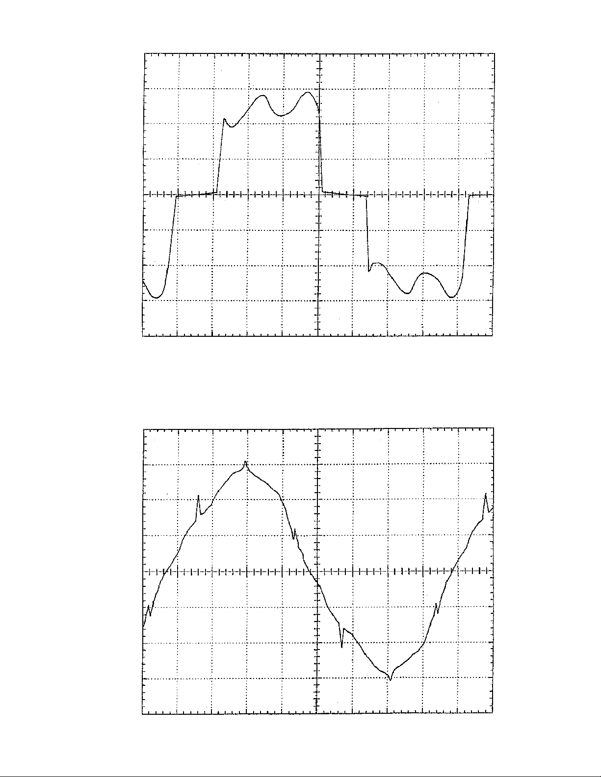
Figure 3A is a plot of the typical input current waveform for
the VSD system without the optional lter when the system
is operating at 50% load. Figure 3B is a plot of the typical
input current waveform for the VSD system with the optional
harmonic lter installed when operating at the same load
conditions. The plots show that the input current waveform
is converted from a square wave to a fairly clean sinusoidal
waveform when the lter is installed. In addition, the power
factor of the system with the optional lter installed corrects
the system power factor to nearly unity.
The power section of the Harmonic Filter is composed of four
major blocks: a pre-charge section, a “trap” lter network,
a three phase inductor and an IGBT Phase Bank Assembly
(See Fig. 4).
The pre-charge section is formed by three resistors (11RES
- 13RES) and two contactors, pre-charge contactor 2M, and
supply contactor 3M. The pre-charge network serves two pur-
poses, to slowly charge the DC link lter capacitors associated
with the lter Phase Bank Assembly (via the diodes within the
IGBT modules Q13-Q18) and to provide a means of discon-
necting the lter power components from the power mains.
When the drive is turned o, both contactors are dropped out
and the lter phase bank assembly is disconnected from the
mains. When the drive is commanded to run, the pre-charge
resistors are switched into the circuit via contactor 2M for a
xed time period of 5 seconds. This permits the lter capac-
itors in the phase bank assembly to slowly charge. After the
5 second time period, the supply contactor is pulled in and
the pre-charge contactor is dropped out, permitting the lter
Phase Bank Assembly to completely charge to the peak of the
input power mains. Three power fuses (11FU -13FU) connect
the lter power components to the power mains. Very fast
semiconductor power fuses are utilized to ensure that the
IGBT modules do not rupture if a catastrophic failure were to

FORM 160.00-O1 (1020)
JOHNSON CONTROLS 9
FIG. 3A – VSD INPUT CURRENT WITHOUT FILTER
FIG. 3B – VSD INPUT CURRENT WITH FILTER
LD02727
LD02726

JOHNSON CONTROLS
10
FORM 160.00-O1 (1020)
occur on the DC link of the lter phase bank assembly.
The “trap” lter is composed of a series of capacitors
(C84-C92), inductors (4L-6L) and resistors (16RES-
18RES). The “trap” lter acts as a low impedance for
a range of frequencies centered at the PWM switching
frequency of the lter (20 KHz). The purpose of the trap
is to block currents at the switching frequency of the lter
from getting onto the power mains.
The three phase inductor provides some impedance
for the lter to “work against”. It eectively limits the
rate of change of current at the input to the lter to a
reasonable level.
The IGBT Phase Bank Assembly is the most compli-
cated power component in the optional lter. Its purpose
is to generate the harmonic currents required by the
VSD’s AC to DC converter so that these harmonic cur-
rents are not drawn from the power mains. The phase
bank is composed of a series of IGBT modules (Q13-
Q18) mounted to a liquid cooled heatsink, a lter ca-
pacitor “bank” (C67-C76) and an IEEE 519 Filter Gate
Driver board (031-01626) which provides the On and O
gating pulses to the IGBT’s as determined by the 519
Filter Logic board. In order to assure an equal sharing
of the voltage between the series connected capacitors
on the lter bank, “bleeder” resistors 14RES and 15RES
are connected across the banks. In order to counteract
the parasitic inductances in the mechanical structure of
the phase bank, the lter incorporates “laminated bus”
technology and a series of small lm capacitors (C77-
C83). The technology used is identical to that used in
the VSD’s DC to AC inverter section of the drive.
Various ancillary sensors and boards are used to convey
information back to the Filter Logic board. A thermistor
temperature sensor RT5 is mounted onto the liquid
cooled heatsink to provide temperature information.
Current Transformers 6T and 7T sense the input current
drawn by the VSD’s AC to DC converter. DC Current
Transformers DCCT1 and DCCT2 sense the current
generated by the optional lter. The Line Voltage Iso-
lation board (031-01625) senses the input voltage to
the system, steps the voltage down to a safe level and
provides isolation between the Filter Logic board and
the power mains. The Bus Isolation board (031-01624)
incorporates three resistors to provide a “safe” impedance
between the DC lter capacitors located on the phase
bank assembly and the Filter logic board. It provides
the means to sense the positive, midpoint and negative
connection points of the lter’s DC link.
VSD CONTROL SYSTEM OVERVIEW
The VSD control system is composed of various com-
ponents located within both the Microcomputer Control
Center and the VSD, thus integrating the Control Center
with the VSD Drive. The VSD system utilizes various
microprocessors and Digital Signal Processors (DSPs)
which are linked together through a network of parallel
and serial communications links.
Micro Computer Control Center
The Microcomputer Control Center contains two boards
that act upon VSD related information, the Microboard
(031-01065) and the Adaptive Capacity Control board
(031-01579). The ACC board performs two major func-
tions in the VSD control system - (1) to act as a gateway
for information ow between the Micro Computer Control
Center and the VSD and (2) to determine the optimum
operating speed and vane position for maximum chiller
system eciency by implementing a totally new and
novel means of Capacity Control.
The ACC board acts as an information gateway for all
data owing between the VSD and the Control Center.
The ACC board communicates serially with both the
VSD logic board (via J8 on the ACC board) and the
optional Harmonic Filter logic board (via J9 on the ACC
board) using a pair of shielded cables. Once the infor-
mation is received by the ACC board, the information is
then passed on to the Microboard via two ribbon cables
connecting the ACC to the Microboard (J1 and J2 on
the ACC board).
In order to achieve the most ecient operation of a
centrifugal compressor, the speed of the compressor
must be reduced to match the “lift” or “head” of the load.
This “lift” or “head” is determined by the chilled and
condenser water temperatures (and their correspond-
ing refrigerant pressures). However, if the compressor
speed is reduced too much, the refrigerant gas will ow
backwards against the compressor wheel causing the
compressor to “surge”, an undesirable and extremely
inecient operating condition. Thus there exists one
particular optimum operating speed (on the “edge” of
surge) for a given head, which provides the optimum
system eciency. The compressor’s inlet guide vanes,
which are used in xed speed applications to throttle
the gas owing through the compressor, are controlled
together with the compressor speed on a VSD chiller
system, to obtain the required chilled water temperature
while simultaneously requiring minimum power from the
power system.

FORM 160.00-O1 (1020)
JOHNSON CONTROLS 11
THIS PAGE INTENTIONALLY LEFT BLANK.

JOHNSON CONTROLS
12
FORM 160.00-O1 (1020)
FIG. 4 – IEEE-519 FILTER OPTION

FORM 160.00-O1 (1020)
JOHNSON CONTROLS 13
LD02725

JOHNSON CONTROLS
14
FORM 160.00-O1 (1020)
The older Turbo-Modulator capacity control boards
utilized a pre-programmed three dimensional surge sur-
face map for each compressor/refrigerant combination;
whereas the new ACC board automatically generates
its own “Adaptive” three dimensional surge surface map
while the chiller system is in operation. This “Adaptive”
operation is accomplished through the use of a patented
surge detection algorithm. The novel surge detection
system utilizes pressure information obtained from the
chillers’ pressure transducers in combination with the
VSD’s instantaneous power output to determine if the
system is in “surge”. Thus the adaptive system permits
construction of a custom compressor map for each
individual chiller system. Benets of this new adaptive
system include: (1) a custom compressor map for each
installation which eliminates inecient operation due to
the safety margin built into the previous programmed
map controller which was necessary to compensate for
compressor manufacturing tolerances (2) the ability to
update the system’s surge surface as the unit ages and
(3) automatic updating of the compressor map if changes
in refrigerant are implemented at a later date.
VSD and Optional Harmonic Filter
Logic Control Boards
Within the VSD enclosure, the VSD logic board and
optional Harmonic Filter logic boards are interconnected
via a 16 position ribbon cable which joins the two boards
together. The Filter Logic board derives its power from
the VSD Logic board over this ribbon cable. In addition
various logic level “handshake” signals convey the oper-
ating status of the VSD to the Filter and vice versa over
this cable. Finally, the cable includes a unidirectional
serial communications link which permits the transmis-
sion of a limited amount of data from the VSD to the
optional Harmonic Filter.
The VSD Logic board performs numerous functions,
including control of the VSD’s cooling fans and pumps,
control of the pre-charge contactor, control of the semi-
converter gating and generation of the PWM ring pulses
which are sent to the VSD gate driver and ultimately gate
the IGBT’s on and o.
The VSD Logic board also gathers data from the Cur-
rent Transformers which monitor the three phases of
motor current, the heatsink temperatures, the internal
ambient temperature within the enclosure and the DC
Link voltage. This data is periodically sent to the Micro
Computer Control Center via the ACC board.
CONTROL PANEL VSD RELATED
KEYPAD FUNCTIONS
The following keypad functions are in addition to the
standard keypad functions as addressed in the standard
chiller literature. The features below are present only
when the control panel is congured for operation with
the VSD:
Options Key – When depressed, the display will
show
VSD 100% JOB FLA = ___ A. . Additional lines of display
are
available by scrolling, using the white key labeled, “Ad-
vance Day / Scroll”. All available lines are listed below:
VSD 100% JOB FLA = ___ A.
VSD DC LINK VOLTAGE = ___V.
VSD DC LINK CURRENT = ___A.
VSD INTERNAL AMBIENT TEMP = ___°F.
VSD CONVERTER HEATSINK TEMP = ___°F.
VSD PHASE A INVERTER HEATSINK TEMP = ___°F.
VSD PHASE B INVERTER HEATSINK TEMP = ___°F.
VSD PHASE C INVERTER HEATSINK TEMP = ___°F.
VSD PRECHARGE RELAY DE-ENERGIZED (or Energized)
VSD SCR GATE DRIVER DISABLED (or Enabled)
VSD COOLING PUMP STOPPED (or Running)
FILTER PRESENT (or Not Present)
When the Filter is Present, these additional lines are
available by scrolling:
FILTER HEATSINK TEMP = ___°F.
FILTER CURR: A=___A.; B=___A.; C=___A.
FILTER DC LINK VOLTAGE = ___V.
INPUT PEAK V.: A=___V.; B=___V.; C=___V.
FILTER STOPPED (Running)
FILTER PRECHARGE RELAY DE-ENERGIZED (Energized)
FILTER SUPPLY RELAY DE-ENERGIZED (Energized)
INPUT PHASE ROTATION - ABC (CBA)
VSD Parameters Key – When this key is pressed,
the VSD output frequency and voltage are displayed.
Additional lines of display are available by pressing the
white key labeled, “Advance Day / Scroll”. All available
lines are listed below:
OUTPUT FREQ __ HZ; OUTPUT VOLTS ___V.
OUTPUT CURR: A=___A.; B=___A.; C=___A.
INPUT POWER = ___KW; KWH = ____________

FORM 160.00-O1 (1020)
JOHNSON CONTROLS 15
Style “B” Units – For the rst time, we have imple-
mented a system which records real-time data, even if
the chiller is not running. Since four power losses, or
four unsuccessful attempts at starting would overwrite
data from the last time the chiller ran, specic history
displays have been generated as follows:
CURRENT OR LAST SYSTEM RUN DATA
LAST SFTY / CYCL SHUTDOWN WHILE RUNNING
SFTY / CYCL SHUTDOWN HISTORY (1)
SFTY / CYCL SHUTDOWN HISTORY (2)
The above lines appear sequentially when the VSD
History Key is depressed. When this key is released,
the message being viewed at that time is maintained.
Using the white “Advance Day / Scroll” key, the Display
Status Message may be viewed, and by continuing to
depress the white “Advance Day / Scroll” key, all VSD
operating data from that instant in time may be viewed.
For example, by depressing the VSD History key once,
you will see:
CURRENT OR LAST SYSTEM RUN DATA
Now by depressing the white “Advance Day / Scroll”
key, you might see:
21 OCT 0804 NO MALFUNCTION DETECTED
Depressing the white “Advance Day / Scroll” key again
will display the rst line of historical data. Continue to
depress the white key to view all lines of data.
“Hidden” Key – There is an unmarked button on the
face of the control panel membrane keypad, located just
below the “Clock” key. When this button is pressed, you
will see a display of four parameters:
DPP = X.XX; PRV = XXX%; LWTD = XX.X; FQ = XX HZ
• D-P/P, the ratio of the condenser pressure minus the
evaporator pressure to the evaporator pressure.
• Percent Vane Position. 100% is wide open vanes.
• Delta T, the dierence between the leaving water
temperature setpoint and actual leaving water tem-
perature.
• Output frequency in hertz.
When the Filter is present, these additional lines are
available by scrolling:
INPUT KVA = ___; TOTAL PWR FACTOR = ____
INPUT V AB=___V.; BC=___V.; CA=___V.
INPUT CURR A=___A.; B=___A.; C=___A.
INPUT V THD: A=___%; B=___%; C=___%
INPUT CURR TDD%: A=___%; B=___%; C=___%
Display Data Key – This key functions as normal, but
oers two additional lines of display with VSD opera-
tion. After scrolling through the normal displays, these
additional lines are displayed:
D-P/P= ___ ; PRV POS = ___%; FREQ = ___HZ
TOTAL ACC SURGE COUNTS = ________
VSD History Key – This key provides four historical
records. Its exact operation varies, depending on the
style level of the VSD and software. The two types of
operation are as follows:
Original and Style “A” Units – Four previous safety /
cycling messages are stored, listing the message, and
indicating the historical order by placing the history num-
ber, one through four, in parenthesis after the message.
Using the white key labeled, “Advance Day / Scroll”,
one can view the same lines of data as are available
by pressing the “Options” and “VSD Parameters” keys.
The data displayed will be that recorded at shutdown,
if running - or will be data from the last time the chiller
ran, if the message was generated while the chiller was
idle. The recording of data from the last time the chiller
ran, is consistent with history data records on all previ-
ous YORK micropanel designs. Below is an example
of four histories:
22 OCT 1501 SERIAL RECEIVE FAULT (1)
21 OCT 1635 SYSTEM CYCLING - AUTOSTART (2)
20 OCT 1000 SYSTEM CYCLING - AUTOSTART (3)
20 OCT 0808 SYSTEM CYCLING - AUTOSTART (4)
These displays will appear sequentially while depress-
ing the VSD History key. When the VSD History key is
released, the message present at that time is maintained
on the screen. With any one of these messages on the
screen, the associated VSD operating data just prior to
unit shutdown may be viewed by scrolling, using the
white “Advance Day / Scroll” key.

JOHNSON CONTROLS
16
FORM 160.00-O1 (1020)
VSD ADAPTIVE CAPACITY CONTROL
The new York VSD utilizes a dierent approach to speed
reduction compared to earlier variable speed products.
There is no pre-programmed surge map - our adaptive
system experiments with the speed and vanes to nd
the optimum speed for any given condition. It does not
always encounter a “Surge” in the process, but when it
does, the ACC stores into memory, the conditions sur-
rounding the Surge, and therefore remembers to avoid
the stored operating point anytime in the future. This
sounds a bit mysterious, but the process is really quite
simple. Once you have an understanding of the steps
involved, you will be able to watch the chiller adjust itself
to dierent conditions, and understand exactly why it is
performing in the manner it does.
Upon startup the chiller will always go to full speed. This
is dierent compared to earlier systems which could go
to a reduced speed if the total head across the chiller
was low enough. With the VSD, the chiller will always
run at xed speed until two conditions are met. These
two conditions are:
Achieve Setpoint - The leaving water temp must
be within +0.3 to -0.6 of a degree from setpoint.
Speed reduction will not occur until the leaving water
reaches setpoint.
Achieve Stability - The leaving water temp must
be stable, with the vanes not driving open or closed
to maintain the temperature at this point. Lack of
stability will be evidenced by the vanes hunting, the
leaving water temperature varying, and the green
LED on the ACC board will be on, to indicate insta-
bility.
Once the above conditions are met, the ACC begins to
lower the speed 1/10 of a hertz at a time. As the ACC
lowers the speed, the leaving water temperature will
begin to creep up, due to the reduction in speed. As this
occurs, you will see the vanes begin to open slightly, just
enough to keep the leaving water temperature within the
setpoint window. The ACC will continue to lower speed,
with the leaving water temperature in turn driving the
vanes to a more open position. This process will continue
until one of three situations occur:
Vanes Full Open - Once the vanes reach the full
open position, the ACC knows it can no longer
reduce speed. The ACC will maintain operation at
this point, with the vanes full-open, and the speed
at the last point reached when the vanes hit 100%.
If there is an increase in load while at this point,
the ACC will increase speed until the vanes are at
95%. The ACC will then be allowed to continue to
optimize the speed and vanes.
Surge is Detected - If in the process of dropping
speed and opening vanes the compressor should
surge, the ACC will boost the speed back up enough
to get the chiller out of surge, and will store in
memory the head and ow conditions present at
the time of the surge. The chiller will then know not
to reduce speed this low again, should the same
head and ow conditions be encountered again in
the future. As the chiller encounters more head and
ow combinations which result in surge, it will store
more points, and eventually this plotting of points
creates a “Surge Map”. Surges may be detected in
two ways, by monitoring the pressure dierential
across the compressor, or by monitoring the com-
pressor motor current. Either detection will light the
Red LED on the ACC board, indicating a surge was
detected. The chiller may surge 6 to 8 times before
the ACC can raise the speed enough to get the
chiller back out of surge. Each surge is counted on
the surge accumulator, which may be called up on
the panel display. This surge counter will always dis-
play the total number of surges encountered by the
chiller, not the total number of surge points. Surging
which occurs at xed speed will increment the surge
counter as well. We know of one chiller which ran
in continuous surge for two weeks due to a cooling
tower problem. The customer’s xed speed chiller
was surging continuously for 2 weeks also. During
this time, the VSD surge counter accumulated over
18,000 surges.
Instability is Encountered - The ACC may begin
the process of reducing speed and opening the
vanes, but may stop speed reduction prematurely
if instability is encountered. This is the same insta-
bility discussed as one of the two conditions which
must be met to begin reducing speed initially (See
“Achieve Stability” above). Once the system again
becomes unstable, no additional speed reduction
can occur. The most common causes of instability
are:
• Valves on air-handler coils causing rapid
changes in heat-load.
• Extremely short chilled water loop.
• Parallel chiller with poor control is causing
temperature variations.
If you experience a problem with a VSD not reducing
speed at all, make certain the system is not in manual
speed control, and locked into xed speed. Refer to the
section on “Manual Speed Control” in the “Frequently
Asked Questions” section in Form 160.00-M1. Also,

FORM 160.00-O1 (1020)
JOHNSON CONTROLS 17
make certain the wiring at J3 on the ACC board is
properly connected per the wiring diagram in this same
manual. Either situation will cause the chiller to maintain
full speed.
If the VSD is reducing speed, but not running as low as
you expect it should, it is likely because it is either in
an unstable condition, or running just above a mapped
surge point. As described above, the chiller must achieve
stability, which is evidenced by the Green LED being
extinguished. Instability will cause the Green LED to
be illuminated. To determine if the chiller is running just
above a surge point, switch the system to manual speed
control, and force the speed lower by one or two hertz.
If you encounter a surge, this explains why the chiller
would not reduce speed. If you nd the chiller does drop
speed without surging, instability was likely preventing
further speed reduction.
VSD DISPLAY MESSAGES
Message: VSD SHUTDOWN - REQUESTING FAULT DATA
This shutdown is initiated when the #53 to #16 circuit
has been interrupted, and the control panel has not
yet received the cause of the fault over the serial link.
Whenever the VSD initiates a fault, it rst opens the
IIS relay in the VSD (between #53 and #16). The VSD
then sends a message serially to the ACC, detailing the
cause of the fault. Since the communications link loop
is initiated every two seconds, the message should ap-
pear for just a few seconds and then be replaced with
a VSD Fault message.
Message: INVERTER INITIATED STOP FAULT
Whenever the VSD initiates a fault, it rst opens the IIS
relay in the VSD (between #53 and #16). It then sends
a message serially to the ACC, detailing the cause of
the fault. If this #53 to #16 circuit ever opens without
receiving an accompanying cause for the trip over the
serial link (within 11 communication tries, approximately
22 seconds) this message will be displayed.
Message: START SEQUENCE INHIBITED BY VSD
This shutdown will occur if a VSD fault takes place dur-
ing the “Start Sequence Initiated” period. The chiller is
inhibited from entering the starting sequence during the
time period that a VSD fault occurs. When the VSD fault
is cleared the start sequence will resume.
Message: PHASE A (OR B,C) OVERCURRENT FAULT
This shutdown is generated by the VSD if the motor cur-
rent exceeds a given limit. The motor current is sensed
by the Current Transformers on the VSD output pole
assemblies and the signals are sent to the VSD logic
board for processing. Maximum instantaneous permis-
sible currents are:
351/292 HP = 771 Amps
503/419 HP = 1200 Amps
790/658 HP = 1890 Amps
1100/900 HP = 3093 Amps
If an overcurrent trip occurs, but the chiller restarts and
runs without a problem, the cause may be attributed to
a voltage sag on the utility power feeding the VSD that
is in excess of the specied dip voltage for this product.
This is especially true if the chiller was running at, or
near, full load. If there should be a sudden dip in line
voltage, the current to the motor will increase, since the
motor wants to draw constant horsepower. The chiller
vanes cannot close quickly enough to correct for this
sudden increase in current, and the chiller will trip on
an overcurrent fault.
If the chiller will not restart, but keeps tripping on this
same shutdown, an output pole problem is the most
likely culprit. The VSD most likely requires service.
Message: PHASE A (B,C) GATE DRIVER FLT
A second level of current protection exists on the VSD
driver boards themselves. The collector-to-emitter
saturation voltage of each IGBT is checked continu-
ously while the device is being gated on. If the voltage
across the IGBT is greater than a set threshold, the
IGBT is gated o and a shutdown pulse is sent to the
VSD logic board shutting down the entire VSD system.
Be aware that a gate driver fault can be initiated when
the VSD is not running.
Message: SINGLE PHASE POWER SUPPLY
This shutdown is generated by the SCR Trigger control
and relayed to the VSD logic board to initiate a system
shutdown. The SCR Trigger control uses circuitry to
detect the loss of any one of the three input phases. The
trigger will detect the loss of a phase within one half line
cycle of the phase loss. This message is also displayed
every time power to the VSD is removed or if the input
power dips to a very low level. Usually it indicates that
someone has opened the disconnect switch.
Message: HIGH PHASE A (B,C) HEATSINK TEMP
This shutdown will occur if the heatsink temperature
exceeds 158°F on any of the output pole assemblies.
This shutdown requires a manual reset via the Reset
push-button on the VSD logic board. This shutdown will
seldom occur, since in most cases where the coolant
temperature has risen abnormally, the VSD will trip on
“Ambient Temperature” (140°F) before the heatsinks

JOHNSON CONTROLS
18
FORM 160.00-O1 (1020)
can reach 158°F. If this message does occur, make
certain you have an adequate level of coolant, check
to be sure the cooling pump is operating when the unit
is running, and check the strainer in the primary of the
heat exchanger for clogs and silt.
Message: HIGH CONVERTER HEATSINK TEMP
Reference “High Phase A (B,C) Heatsink Temp” above.
This shutdown requires a manual reset via the Reset
push-button on the VSD logic board.
Message: 105% MOTOR CURRENT OVERLOAD
This shutdown is generated by the VSD logic board
and it indicates that a motor overload has occurred.
The shutdown is generated when the VSD logic board
has detected that at least one of the three output phase
currents has exceeded 105% of the programmed 100%
job full load amps (FLA) value. The 100% job FLA
setpoint may be viewed by pressing the “Options” key.
This shutdown requires a manual reset via the Reset
push-button on the VSD logic board.
Message: BUS OVER-VOLTAGE FAULT
The VSD’s DC link voltage is continuously monitored
and if the level exceeds 745 VDC, a Bus Over-Voltage
shutdown is initiated. If this shutdown occurs, it will be
necessary to look at the level of the 460 VAC applied to
the drive. The specied voltage range is 414 to 508. If
the incoming voltage is in excess of 508, steps should be
taken to reduce the voltage within the specied limits.
Message: MAIN BOARD POWER SUPPLY
This shutdown is generated by the VSD logic board
and it indicates that the low voltage power supplies for
the logic boards have dropped below their allowable
operating limits. The power supplies for the logic boards
are derived from the secondary of the 120 to 24 VAC
transformer (Fig. 2) which in turn is derived from the 480
to 120 VAC control transformer (Fig. 1). This message
usually means that power to the VSD was removed.
Message: LOW DC BUS VOLTAGE FLT
If the DC link drops below 500 VDC (or 414 VDC for 50
HZ), the drive will initiate a system shutdown. A common
cause for this shutdown is a severe sag in the incoming
power to the drive. Monitor the incoming three phase
AC line for severe sags and also monitor the DC link
with a digital meter.
Message: BUS VOLTAGE IMBALANCE FAULT
The DC link is ltered by many large, electrolytic capaci-
tors which are rated for 450 VDC. These capacitors are
wired in series to achieve a 900 VDC capability for the
DC link. It is important that the voltage be shared equally
from the junction of the center or series capacitor con-
nection, to the negative bus and to the positive bus. This
center point should be approximately ½ of the total DC
link voltage. Most actual bus voltage imbalance conditions
are caused by a shorted capacitor, or a leaky or shorted
IGBT transistor in an output phase bank assembly. This
usually indicates the VSD requires service.
Message: HIGH AMBIENT TEMPERATURE FLT
The ambient temperature monitored is actually the
temperature detected by a component mounted on the
VSD logic board. The high ambient trip threshold is set
for 140°F. Some potential causes for this shutdown are:
internal VSD fan failure, VSD water pump failure or an
entering condenser water temperature which exceeds
the allowable limit for the job. Additional causes for the
shutdown include:
• Plugged Strainer – The standard 1.5” Y-Strainer con-
tains a woven wire mesh element with 20 stainless-
steel wires per inch. This has been found to work
adequately in most applications. Some users may
have very dirty condenser water which can cause the
strainer to plug. Locations with special conditions
may want to consider a dual strainer arrangement
with quarter turn valves, to permit cleaning of one
strainer with the unit still on-line.
• Plugged Heat-Exchanger – In cases where the
strainer plugs frequently, the heat-exchanger
eventually may plug or become restricted to the
point of reduced ow. At this point we suggest you
back-ush the heat-exchanger by reversing the two
rubber hoses which supply condenser water to/from
the heat-exchanger. If the rust or sludge cannot be
back-ushed, you may need to replace the heat-
exchanger.
• Low Condenser Flow – The VSD system requires
8 feet of pressure drop across the heat exchanger
to maintain adequate GPM. If the pressure drop is
less than 8 feet, it will be necessary to correct the
ow problem, or add a booster pump as is applied
on retrot chillers.
Message: INVALID CURRENT SCALE FAULT
Since the part number of the logic board is the same
on all horsepower sizes, jumpers tell the logic board
the size of the VSD being employed in order to properly
scale the output current. If the jumper conguration is
found by the logic to be invalid, the system will be shut
down and the above message will be generated. The
proper jumper conguration is shown on the wiring label
for the VSD.

FORM 160.00-O1 (1020)
JOHNSON CONTROLS 19
Message: LOW (CONV, OR PHASE A,B,C) HEATSINK TEMP.
A heatsink temperature sensor indicating a temperature
below 37°F will cause the unit to shut down and display
this message. In most cases the problem will actually
be an open thermistor or broken wiring to the thermis-
tor. The normal thermistor resistance is 10K ohms at
70°F.
Message: OUTPUT CURRENT IMBALANCE
Normally the three phases of output current will be
closely balanced since the voltage being applied to the
motor is derived from the same DC Link voltage and the
output transistors all switch in an identical pattern. Thus
most imbalances will be due to variations in the motor
windings, which may be as high as 8% typically.
Message: PRECHARGE BUS V IMBALANCE
This situation is identical to the above shutdown, “Bus
Voltage Imbalance Flt”, except that it has occurred during
the precharge period which begins during pre-lube.
Message: PRECHARGE LOW VOLTAGE FAULT
During precharge the DC Link must be equal to or greater
than 50 VDC (41 VDC for 50 HZ) ½ second after the pre-
charge relay is energized. The unit is shut down and this
message is generated if this condition is not met.
Message: PRE-CHARGE HIGH VOLTAGE FAULT
During precharge the DC Link must reach at least 500
VDC (414 VDC for 50 HZ) 15 seconds after the pre-
charge relay is energized. The unit is shut down and this
message is generated if this condition is not met.
Message: PRE-CHARGE FAULT LOCKOUT
If the unit fails to make pre-charge, the pre-charge relay
shall drop out for a time period of 10 seconds during
which time the units fan(s) and water pump(s) shall
remain energized in order to permit the pre-charge
resistors to cool. Following this 10-second cool down
period pre-charge shall again be initiated. The unit shall
attempt to make pre-charge three consecutive times.
If the unit fails to make pre-charge on three consecu-
tive tries, the unit will shut down, lockout and display
this message. In order to initiate pre-charge again, the
Micropanel’s rocker switch must rst be placed into the
STOP/RESET position.
Message: PWM COMMUNICATIONS FAULT
This shutdown is generated if a communications prob-
lem occurs between the two microprocessors on the
VSD logic board.
Message: RUN RELAY FAULT
Redundant run signals are generated by the Micropanel,
one via wire #24 and the second via the serial communica-
tions link. Upon receipt of either of the two run commands
by the VSD logic board, a 5-second timer shall commence
timing. If the missing run command is not asserted within
the 5-second window the unit will shut down and the
Micropanel will display the message Run Relay Fault.
This shutdown could occur if there is a problem with the
wiring between the control panel and the VSD.
Message: SERIAL RECEIVE FAULT
This message is generated when communications be-
tween the ACC and VSD logic is disrupted. Check the
shielded cable between J11 on the VSD logic and J8 on
the ACC board. If all wiring is intact, this problem may
also be caused by electrical noise.
Message: VSD INITIALIZATION FAILED
At power-up, all the boards go through a process called
initialization. At this time, memory locations are cleared,
jumper positions are checked, and serial communica-
tions links are established. There are many causes for
an unsuccessful initialization. The following check-list
should aid in determining why initialization has not
completed:
• The Micro-Panel and the VSD must be energized
at the same time. The practice of pulling the fuse in
the control panel to make wiring changes will create
a problem. Power-up must be done by closing the
main disconnect on the VSD cabinet with all fuses
in place. Be sure you do not have a blown fuse,
causing loss of power to the VSD logic board.
• The EPROMs must be correct for each board, and
they must be correctly installed. There are a total
of seven (7) EPROMs in each VSD - Micropanel
system. These EPROMs are created as a set, and
cannot be intermixed between earlier and later
styles of units. Also, the ACC EPROM must be in
the ACC board, and the Micropanel EPROM in the
Microboard, etc. All pins must be properly inserted
into the EPROM sockets.
• Serial data communications must be established.
See the write ups for the messages, “Serial Receive
Fault” and “FLTR Serial Receive Fault” (Pages 13
& 16). If communications among the VSD logic, the
lter logic, the ACC and the Microboard does not
take place at initialization, the “VSD Initialization
Failed” message will occur before any other mes-
sage can be generated. You can check to see that
serial communications have been established by

JOHNSON CONTROLS
20
FORM 160.00-O1 (1020)
pressing the OPTIONS key and noting the %Job
FLA value displayed. A zero displayed value for this
parameter (and all other VSD parameters) indicates
a serial communications link or EPROM problem.
• If the IEEE-519 Filter option is included, make sure
the ‘519’ Logic board is not in continuous reset.
This will be evidenced by the LEDs on the lter logic
board alternately blinking. To rule out the ‘519’ lter
as the cause of initialization failure, you can discon-
nect the lter by switching the lter logic board’s
SW1 switch to the OFF position, and removing the
16 wire ribbon cable between the ‘519’ logic and
VSD logic boards.
Message: FLTR HEATSINK OVERTEMP FLT
The ‘519’ filter power assembly has one heatsink
thermistor on the 351 & 503 HP units, and two heatsink
thermistors on the 790 HP units. If the temperature on
any heatsink exceeds 167 °F, the unit will shut down,
and require a manual reset by pressing the “Overtemp
Reset” pushbutton located on the Filter Logic board.
This message is usually an indication that the level of
coolant in the closed loop system on the back of the
VSD is low.
Message: FLTR BUS OVER-VOLTAGE FLT
The harmonic lter’s DC link voltage is continuously
monitored and if the level exceeds a level of 860 VDC
a Filter Bus Over-Voltage shutdown is initiated. Keep
in mind that the harmonic lter has its own DC bus as
part of the lter power assembly, and this DC Link is
not connected in any way with the drive’s DC Link. If
this shutdown occurs, it will be necessary to look at the
level of the 460 VAC applied to the drive. The specied
voltage range is 414 to 508. If the incoming voltage is
in excess of 508, steps should be taken to reduce the
voltage within the specied limits. The cause of this
message will typically be high line voltage, or a surge
on the utility supply.
Message: FLTR LOW BUS VOLTAGE FLT
The harmonic lter dynamically generates its own lter
DC link voltage by switching its IGBT’s. This DC level
is actually higher than the level that one could obtain
by simply rectifying the input line voltage. Thus the har-
monic lter actually performs a voltage “boost” function.
This is necessary in order to permit current to ow into
the power line from the lter when the input line is at its
peak level. This particular shutdown and its accompany-
ing message is generated if the lter’s DC link voltage
drops to a level less than 60 VDC below the lter DC
link voltage setpoint. The lter DC link voltage setpoint
is determined by the lter logic board via the sensing of
the three phase input line-to-line voltage. This setpoint
is set to the peak of the sensed input line- to-line voltage
plus 32 volts, not to exceed 760 volts and varies with
the input line-to-line voltage. If this shutdown occurs
occasionally, the likely cause is a severe sag in the
input line voltage. A power monitor should be installed
to determine if a power problem exists.
Message: FLTR PHASE A (B,C) OVERCURRENT
The maximum instantaneous harmonic lter current is
monitored and compared against a preset limit. If this
limit is exceeded, the unit is shut down and this mes-
sage is generated. The lter current is monitored using
two DCCTs and these signals are processed by the lter
logic board. The preset limits are as follows:
351/292 HP = 378 Amps
503/419 HP = 523 Amps
790/658 HP = 782 Amps
1100/900 HP = 1225 Amps
If you experience this shutdown and the VSD auto-
restarts and continues to run properly with the lter
operating, it is likely the lter tripped on Overcurrent due
to a sag or surge in the voltage feeding the chiller. If
this message re-occurs, preventing the unit from being
restarted, the VSD will require service.
Message: FLTR PHASE LOCK LOOP FLT
This shutdown indicates that a circuit called a “phase
locked loop” on the lter logic board has lost synchro-
nization with the incoming power line for a period of
time. This is normally an indication that one of the lter’s
incoming power fuses is blown. Check lter power fuses
11FU, 12FU and 13FU if this shutdown occurs.
Message: FLTR POWER SUPPLY FLT
This shutdown indicates that the low voltage power
supplies on the lter logic board have dropped below
their permissible operating voltage range. The lter logic
board receives its power from the VSD logic board via
the ribbon cable which connects the two boards.
Message: FLTR BUS V IMBALANCE FLT
The lter DC link is ltered by large, electrolytic capaci-
tors which are rated for 450 VDC. These capacitors
are wired in series to achieve a 900 VDC capability for
the DC link. It is important that the voltage be shared
equally from the junction of the center or series capacitor
connection, to the negative bus and to the positive bus.
This center point should be approximately ½ of the total
DC link voltage.
This manual suits for next models
23
Table of contents
Other York DC Drive manuals
Popular DC Drive manuals by other brands

Sprint Electric
Sprint Electric 400 product manual

YASKAWA
YASKAWA SI-T3 MECHATROLINK-II A1000 Series installation manual

AMCI
AMCI SD17040C user manual

Power Electronics
Power Electronics SD 500 Series manual

Siemens
Siemens MICRO MASTER Junior operating instructions

Beijer Electronics
Beijer Electronics BFI-H3 Start-up