Zynq UltraScale+ User manual

Zynq UltraScale+ RFSoC
RF Data Converter
Evaluation Tool (ZCU111)
User Guide
UG1287 (v2018.2) October 1, 2018

RFSoC Data Converter Evaluation Tool User Guide 2
UG1287 (v2018.2) October 1, 2018 www.xilinx.com
Revision History
The following table shows the revision history for this document.
Section Revision Summary
10/01/2018 Version 2018.2
DAC Data Flow Added information about feeding data to the RF-DAC.
Streaming MUX Added channel control selection information.
GPIO Selection Replaced Table 3-2.
Application Flow Added DDR and BRAM selection information and
information to start DMA.
DAC Flow for PL DDR Added this section.
Example Commands and Responses Added commands to Table A-1.
08/14/2018 Version 2018.2
Initial Xilinx release N/A
Send Feedback

RFSoC Data Converter Evaluation Tool User Guide 3
UG1287 (v2018.2) October 1, 2018 www.xilinx.com
Table of Contents
Revision History . . . . . . . . . . . . . . . . . . . . . . . . . . . . . . . . . . . . . . . . . . . . . . . . . . . . . . . . . . . . . . . . . . . . 2
Chapter 1: Introduction
Overview . . . . . . . . . . . . . . . . . . . . . . . . . . . . . . . . . . . . . . . . . . . . . . . . . . . . . . . . . . . . . . . . . . . . . . . . 5
Zynq UltraScale+ RFSoC Overview . . . . . . . . . . . . . . . . . . . . . . . . . . . . . . . . . . . . . . . . . . . . . . . . . . . . 7
Reference Design Overview . . . . . . . . . . . . . . . . . . . . . . . . . . . . . . . . . . . . . . . . . . . . . . . . . . . . . . . . . 9
Chapter 2: Package Details
Chapter 3: Hardware Design
Hardware Overview. . . . . . . . . . . . . . . . . . . . . . . . . . . . . . . . . . . . . . . . . . . . . . . . . . . . . . . . . . . . . . . 14
DAC Data Flow . . . . . . . . . . . . . . . . . . . . . . . . . . . . . . . . . . . . . . . . . . . . . . . . . . . . . . . . . . . . . . . . . . . 15
ADC Data Flow . . . . . . . . . . . . . . . . . . . . . . . . . . . . . . . . . . . . . . . . . . . . . . . . . . . . . . . . . . . . . . . . . . . 21
Stream Pipes Control and Status Registers . . . . . . . . . . . . . . . . . . . . . . . . . . . . . . . . . . . . . . . . . . . . 24
GPIO Selection . . . . . . . . . . . . . . . . . . . . . . . . . . . . . . . . . . . . . . . . . . . . . . . . . . . . . . . . . . . . . . . . . . . 24
Chapter 4: Clocking
Clock Switching . . . . . . . . . . . . . . . . . . . . . . . . . . . . . . . . . . . . . . . . . . . . . . . . . . . . . . . . . . . . . . . . . . 28
Resets . . . . . . . . . . . . . . . . . . . . . . . . . . . . . . . . . . . . . . . . . . . . . . . . . . . . . . . . . . . . . . . . . . . . . . . . . . 34
Chapter 5: Evaluation Tool System Configuration using the GUI
External Component Configuration . . . . . . . . . . . . . . . . . . . . . . . . . . . . . . . . . . . . . . . . . . . . . . . . . . 37
ADC Configuration . . . . . . . . . . . . . . . . . . . . . . . . . . . . . . . . . . . . . . . . . . . . . . . . . . . . . . . . . . . . . . . . 38
ADC Clock Configuration . . . . . . . . . . . . . . . . . . . . . . . . . . . . . . . . . . . . . . . . . . . . . . . . . . . . . . . . . . . 41
Digital Down Converter Configurations . . . . . . . . . . . . . . . . . . . . . . . . . . . . . . . . . . . . . . . . . . . . . . . 42
DAC Configuration . . . . . . . . . . . . . . . . . . . . . . . . . . . . . . . . . . . . . . . . . . . . . . . . . . . . . . . . . . . . . . . . 42
DAC Clock Configurations . . . . . . . . . . . . . . . . . . . . . . . . . . . . . . . . . . . . . . . . . . . . . . . . . . . . . . . . . . 42
Digital Up Converter Configurations. . . . . . . . . . . . . . . . . . . . . . . . . . . . . . . . . . . . . . . . . . . . . . . . . . 43
ADC Tone Testing . . . . . . . . . . . . . . . . . . . . . . . . . . . . . . . . . . . . . . . . . . . . . . . . . . . . . . . . . . . . . . . . . 43
Chapter 6: Software Architecture
Software Architecture . . . . . . . . . . . . . . . . . . . . . . . . . . . . . . . . . . . . . . . . . . . . . . . . . . . . . . . . . . . . . 45
Send Feedback

RFSoC Data Converter Evaluation Tool User Guide 4
UG1287 (v2018.2) October 1, 2018 www.xilinx.com
Chapter 7: Protocol Specification
Socket Interface . . . . . . . . . . . . . . . . . . . . . . . . . . . . . . . . . . . . . . . . . . . . . . . . . . . . . . . . . . . . . . . . . . 49
Command Types. . . . . . . . . . . . . . . . . . . . . . . . . . . . . . . . . . . . . . . . . . . . . . . . . . . . . . . . . . . . . . . . . . 51
Application Flow . . . . . . . . . . . . . . . . . . . . . . . . . . . . . . . . . . . . . . . . . . . . . . . . . . . . . . . . . . . . . . . . . 51
Multi-Tile Sync . . . . . . . . . . . . . . . . . . . . . . . . . . . . . . . . . . . . . . . . . . . . . . . . . . . . . . . . . . . . . . . . . . . 54
Chapter 8: Zynq UltraScale+ RFSoC Data Converter Bare-metal/Linux Driver
Chapter 9: System Considerations
Boot Process. . . . . . . . . . . . . . . . . . . . . . . . . . . . . . . . . . . . . . . . . . . . . . . . . . . . . . . . . . . . . . . . . . . . . 59
Global Address Map. . . . . . . . . . . . . . . . . . . . . . . . . . . . . . . . . . . . . . . . . . . . . . . . . . . . . . . . . . . . . . . 60
Memory . . . . . . . . . . . . . . . . . . . . . . . . . . . . . . . . . . . . . . . . . . . . . . . . . . . . . . . . . . . . . . . . . . . . . . . . 60
Memory Mapping for RF-DAC/RF-ADC. . . . . . . . . . . . . . . . . . . . . . . . . . . . . . . . . . . . . . . . . . . . . . . . 61
Appendix A: Reference Design Protocol Specification
Commands . . . . . . . . . . . . . . . . . . . . . . . . . . . . . . . . . . . . . . . . . . . . . . . . . . . . . . . . . . . . . . . . . . . . . . 62
Example Commands and Responses . . . . . . . . . . . . . . . . . . . . . . . . . . . . . . . . . . . . . . . . . . . . . . . . . 64
Control Path Core Implementation . . . . . . . . . . . . . . . . . . . . . . . . . . . . . . . . . . . . . . . . . . . . . . . . . . 65
Appendix B: Additional Resources and Legal Notices
Xilinx Resources . . . . . . . . . . . . . . . . . . . . . . . . . . . . . . . . . . . . . . . . . . . . . . . . . . . . . . . . . . . . . . . . . . 68
Solution Centers. . . . . . . . . . . . . . . . . . . . . . . . . . . . . . . . . . . . . . . . . . . . . . . . . . . . . . . . . . . . . . . . . . 68
Documentation Navigator and Design Hubs . . . . . . . . . . . . . . . . . . . . . . . . . . . . . . . . . . . . . . . . . . . 68
References . . . . . . . . . . . . . . . . . . . . . . . . . . . . . . . . . . . . . . . . . . . . . . . . . . . . . . . . . . . . . . . . . . . . . . 69
Please Read: Important Legal Notices . . . . . . . . . . . . . . . . . . . . . . . . . . . . . . . . . . . . . . . . . . . . . . . . 70
Send Feedback

RFSoC Data Converter Evaluation Tool User Guide 5
UG1287 (v2018.2) October 1, 2018 www.xilinx.com
Chapter 1
Introduction
Overview
The objective of this reference design is to help you quickly and easily evaluate the new RF
Data Converter (DC) Evaluation Tool functionality in the Zynq® UltraScale+™ family of
RFSoCs. The RFSoC design demonstrates the capabilities and performance of the RF data
converter (RFDC—RF-ADC and RF-DAC) available in the RFSoC devices. The evaluation tool
serves as a platform for you to evaluate the Zynq UltraScale+ RFSoC features and helps
accelerate the product design cycle.
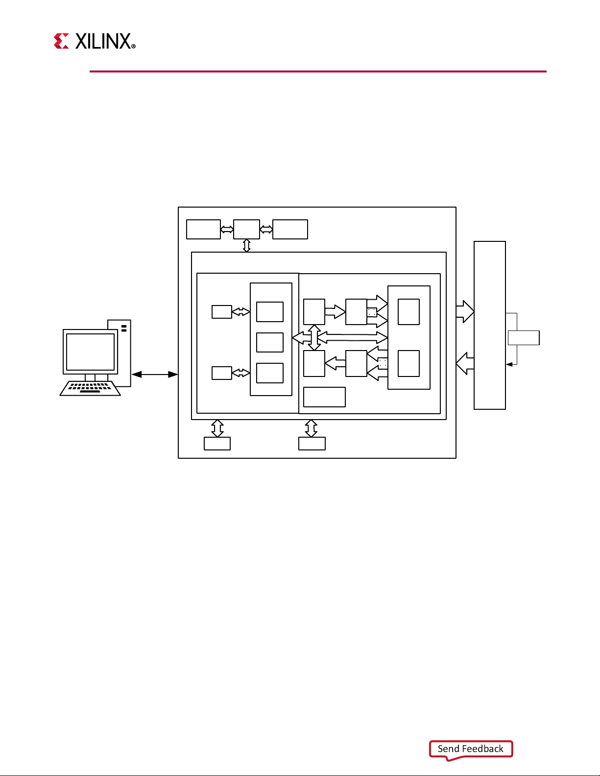
The evaluation tool consists of a ZCU111 evaluation board and a custom-developed
graphical user interface (GUI) installed on a Windows host machine. The evaluation tool
allows you to configure the operation of the RF-ADCs and RF-DACs and perform some basic
tests e.g., FFT analysis of the ADC output for various input test signals. The key
differentiator of Zynq UltraScale+ RFSoC devices when compared to many other discrete
solutions is that the device contains both RF-ADCs and RF-DACs. However, one significant
benefit is the DACs can be used to provide test signals for the ADC (i.e., loopback) which
facilitates a very compact and easy to use solution for early demonstration or evaluation.
All communications to the host PC (GUI) use the processing system (PS) Ethernet interface.
This is necessary to facilitate the transfer of a large amount of test data as efficiently as
possible. The ZCU111 evaluation board supports an external DDR4 memory interface on the
programmable logic (PL) in addition to the PS DDR4 memory. Waveforms with a limited
number of samples can leverage on-chip memory, but application testing and prototyping
require the use of much larger external memories.
The Xilinx® Vivado® IP integrator flow is used to create the hardware design, which is
partitioned between the PS, RFDC, and PL. The reference design uses the IP integrator core
for the RF Data Converter subsystem. The implementation supports all data rates on PL to
the Data Converter interface, all converter sample rates and digital up conversion
(DUC)/digital down conversion (DDC) configurations with a single design. The Xilinx
PetaLinux flow is used to create and integrate the software components, including the Linux
kernel and drivers.
Send Feedback

RFSoC Data Converter Evaluation Tool User Guide 6
UG1287 (v2018.2) October 1, 2018 www.xilinx.com
Chapter 1: Introduction
This user guide describes the architecture of the design and provides a functional
description of its components. It is organized as follows:
Chapter 1, Introduction (this chapter) provides a high-level overview of the Zynq
UltraScale+ RFSoC device architecture, the design architecture, and a summary of key
features.
Chapter 2, Package Details gives an overview of the design modules and design
components that make up this design.
Chapter 3, Hardware Design describes the hardware platform of the design including
key PS and PL peripherals.
Chapter 4, Clocking describes the details on clocking used for the design.
Chapter 5, Evaluation Tool System Configuration using the GUI describes the details of
system configuration and features supported using the GUI.
Chapter 6, Software Architecture describes the application processor unit (APU)
software platform including the Linux software stack and the Linux rftool application
running on the APU.
Chapter 7, Protocol Specification describes the protocol used to communicate between
the host and RFSoC.
Chapter 8, Zynq UltraScale+ RFSoC Data Converter Bare-metal/Linux Driver describes
where to get more information about the driver.
Chapter 9, System Considerations describes system architecture considerations
including boot flow and the system address map.
Appendix A, Reference Design Protocol Specification describes the commands used in
the software design.
Appendix B, Additional Resources and Legal Notices lists additional resources and
references.
Send Feedback

RFSoC Data Converter Evaluation Tool User Guide 7
UG1287 (v2018.2) October 1, 2018 www.xilinx.com
Chapter 1: Introduction
Zynq UltraScale+ RFSoC Overview
The Zynq UltraScale+ RFSoC family integrates the key subsystems required to implement a
complete software-defined radio including direct RF sampling data converters, enabling
CPRI and Gigabit Ethernet-to-RF on a single, highly programmable SoC.
Each RFSoC offers multiple RF-sampling analog-to-digital (RF-ADC) and RF-sampling
digital-to-analog (RF-DAC) data converters. The RF-ADC supports a maximum sample rate
of 4 GSPS with dynamic range and has a signal bandwidth of up to 4 GHz. The RF-DAC can
clock at up to 6.554 GSPS with an output signal bandwidth of greater than 4 GHz. The RF
data converters also include power efficient digital down converters (DDCs) and digital up
converters (DUCs) that include programmable interpolation, decimation rates, a
numerically controlled oscillator (NCO), and a complex mixer. The DDCs and DUCs can also
support multi-band operation. Figure 1-1 shows the block diagram of the Zynq UltraScale+
RFSoC RF Data Converter.
X-Ref Target - Figure 1-1
Figure 1-1: Zynq UltraScale+ RFSoC RF Data Converter in RFSoC
Zynq UltraScale+ RFSoC
Control and
Configuration
Data Converter IP Core
Processing System
Quad ARM Cortex-A53
Dual ARM Cortex-R5
GTY Serial
Transceivers
Programmable
Logic
DUC
AXI4-Stream
DUC
AXI4-Stream
8 TX Channels
DDC
AXI4-Stream
DDC
AXI4-Stream
8 RX Channels
AXI4-Lite
DAC
DAC
ADC
ADC
X21232-092118
Send Feedback

RFSoC Data Converter Evaluation Tool User Guide 8
UG1287 (v2018.2) October 1, 2018 www.xilinx.com
Chapter 1: Introduction
The RF-ADCs and RF-DACs are organized into tiles, each containing either two or four
RF-ADCs or four RF-DACs (see Figure 1-2). Each tile also includes a block with a PLL and all
the necessary clock handling logic and distribution routing for the analog and digital logic.
For device specifications and additional information, see:
•Zynq UltraScale+ RFSoC Data Sheet: Overview (DS889) [Ref 1]
•Zynq UltraScale+ RFSoC Data Sheet: DC and AC Switching Characteristics (DS926)
[Ref 2]
•Zynq UltraScale+ Device Technical Reference Manual (UG1085) [Ref 3].
X-Ref Target - Figure 1-2
Figure 1-2: Converter Tile Structure
DAC_X0Y0
Data Path 2
Data Path 3
Data Path 1 DAC1
Data Path 0 DAC0
IP State
Machine
s03_axis
s02_axis
s01_axis
s00_axis
6.4 GSPS RF-DAC Tile
ADC_X0Y1
Data Path 2 ADC2
Data Path 3 ADC3
Data Path 1 ADC1
Data Path 0 ADC0
m13_axis
m12_axis
m11_axis
m10_axis
2 GSPS RF-ADC Tile
ADC_X0Y0
Data Path 1
(23)
ADC1
(23)
Data Path 0
(01)
ADC0
(01)
m03_axis
m02_axis
m01_axis
m00_axis
4 GSPS RF-ADC Tile
IP State
Machine
IP State
Machine
DAC2
DAC3
X21300-090918
Send Feedback

RFSoC Data Converter Evaluation Tool User Guide 9
UG1287 (v2018.2) October 1, 2018 www.xilinx.com
Chapter 1: Introduction
Reference Design Overview
The evaluation tool targets the Zynq UltraScale+ RFSoC ZU28DR-FFVG1517 running on the
ZCU111 evaluation board and provides a platform to evaluate the RFSoC features. The
system level block diagram of the evaluation tool design is shown in Figure 1-3.
The evaluation tool uses an integrated RF Data Converter in an 8x8 configuration along with
AXI DMA and AXI4-Stream components for high performance data transfers between
PL-DDR to RFDC and vice versa. Stream Pipe comprises various AXI4-Stream Infrastructure
IPs. The AXI DMA is configured in Scatter Gather (SG) mode for high performance. The
evaluation tool also makes use of multiple processing units available inside the PS, such as
Gigabit Ethernet, I2C, and SD Interface. The APU inside the PS is configured to run in
symmetric multiprocessing (SMP) Linux mode. The main task of the Linux application is to
configure and control the RF-ADC and RF-DAC blocks and the flow of data through the
streaming pipeline.
A custom-developed Windows-based GUI is provided along with this evaluation tool. It can
interact with the RFSoC device running on the ZCU111 evaluation board. The GUI connects
to the Linux application running on the RFSoC via a TCP Ethernet interface. Based on
X-Ref Target - Figure 1-3
Figure 1-3: RF Data Converter Evaluation Tool System Level Block Diagram
PL DDR
AXIS
AXIS
DMA
AXIS
AXIS
AXI
AXI4-Lite
I2C
Mux
Clock
Module
Power
Controller
Processing System Programmable Logic
Clocking
and Control
PC User
Interface Gigabit
Ethernet AXIS
AXIS
Zynq® UltraScale+™ RFSoC
ZCU111 Evaluation Board
Daughter
Card
(HW-
RFMC-
XM500)
RFdc IP
DAC
ADC
GEM
I2C
Software
Application
Stream
Pipes
Stream
Pipes
DMA
DMA
PL DDRPS DDR
I2C Driver
RFdo
Driver
GEM
Driver
$38
Filters
X21291-092118
Send Feedback

RFSoC Data Converter Evaluation Tool User Guide 10
UG1287 (v2018.2) October 1, 2018 www.xilinx.com
Chapter 1: Introduction
commands received from the GUI, the Linux application performs various operations that
are described in Chapter 6, Software Architecture. Because a TCP socket is used to transfer
the data over Ethernet, it is possible to run the GUI on any machine connected to the
network (i.e., cloud).
The evaluation tool can be run in three separate modes:
Standalone DAC: In this mode, a pattern is generated using the GUI on the host
machine. This pattern is constantly replayed on the selected DAC channel. The output of
the DAC can be monitored on any standard external equipment, such as a spectrum
analyzer or oscilloscope.
Standalone ADC: In this mode, you generate an analog signal from external equipment,
and this signal is fed to ADC inputs. Digital output of the ADC can be analyzed on the
host machine using the GUI.
DAC to ADC Loopback: In this mode, the output of the DAC is looped back to the input
of ADC. In this way, you can generate a pattern on DAC from the GUI and can analyze the
same pattern on ADC output in the GUI. It is recommended to manage RF signal
conditioning well. Anti-aliasing filters are supplied in the ZCU111 development kit for
the existing RF line up of RFMC-XM500.
Note: For system performance and limitations in various scenarios, see the ZCU111 RFSoC RF Data
Converter Evaluation Tool Getting Started Guide [Ref 4].
Components
• Evaluation platform
°ZCU111 evaluation board
°Daughter card (HW-FMC-XM500)
°Cables and filters (see the Zynq UltraScale+ RFSoC ZCU111 Evaluation Kit Quick
Start Guide (XTP490) [Ref 5]
• Xilinx tools
°Vivado® Design Suite 2018.2 [Ref 6]
°Xilinx® Software Development Kit (XSDK) 2018.2 [Ref 7]
°PetaLinux tools 2018.2 [Ref 8]
• Hardware interfaces and IP
°RFDC
°AXI DMA
°DDR controller interface
°AXI SmartConnect
Send Feedback

RFSoC Data Converter Evaluation Tool User Guide 11
UG1287 (v2018.2) October 1, 2018 www.xilinx.com
Chapter 1: Introduction
°AXI interconnect
°AXI Streaming IPs
• Auxiliary peripherals
°SD
°I2C
°PS-GPIO
°Gigabit Ethernet
°UART
°JTAG
Software Components
• Operating systems
°APU: SMP Linux
• Linux frameworks
°Ethernet
°Clock
°Contiguous memory allocator (CMA)
• User applications
°APU: Ethernet-based server application
• RFDC driver-based features
°Digital down conversion (DDC)/digital up conversion (DUC)
°Nyquist Mix mode
°Digital complex mixers
°Quadrature modulation correction (QMC)
°Internal PLL
°ADC calibration
°DAC high linearity and low noise
°Inverse sinc filter
°DAC Output Current mode (20 or 32 mA)
°External clock driver
• AXI-DMA client driver
Send Feedback

RFSoC Data Converter Evaluation Tool User Guide 13
UG1287 (v2018.2) October 1, 2018 www.xilinx.com
Chapter 2
Package Details
The evaluation tool ZIP file package
rdf0476-zcu111-rf-dc-eval-tool-2018-2.zip
contains the following components grouped by application processor unit (APU) or
programmable logic (PL).
APU
petalinux_bsp: PetaLinux board support package (BSP) is included to build a
pre-configured SMP Linux image for the APU. The BSP includes the following components:
• First stage boot loader (FSBL)
• ARM trusted firmware (ATF)
•U-Boot
• Linux kernel
• Device tree
• Root file system (rootfs)
PL
Vivado: Vivado IP integrator design that integrates the RF Data Converter subsystem, AXI
DMA, Stream Pipe, AXI Interconnect, and PL DDR controller.
Host System GUI
The user interface connecting to the ZCU111 platform via Ethernet cable.
Send Feedback

RFSoC Data Converter Evaluation Tool User Guide 14
UG1287 (v2018.2) October 1, 2018 www.xilinx.com
Chapter 3
Hardware Design
Hardware Overview
The Vivado IP integrator flow is used to create the hardware design which is partitioned
between the processing system (PS), RF Data Converter (RFDC), and programmable logic
(PL). Figure 3-1 shows the hardware block diagram.
X-Ref Target - Figure 3-1
Figure 3-1: Hardware Block Diagram
S_AXI_HP0_FPD S_AXI_HP1_FPD M_AXI_HPM0_FPD
Programmable Logic
Stream Pipe
ADC0
Channel Select Mux
ADC7
DMA
Stream Pipe
Stream Mux
DMA
DAC0 DAC7
RFdc
AXI Interconnect AXI Interconnect
DDR4 Controller (MIG)
AXI Smartconnect
AXI Interconnect
DDR
Controller GEM SD I2C
APU
APU
APU
APU
Processing System
Clocking and Control
GPIOs
Stream Pipe Stream Pipe
X21233-092118
Send Feedback

RFSoC Data Converter Evaluation Tool User Guide 15
UG1287 (v2018.2) October 1, 2018 www.xilinx.com
Chapter 3: Hardware Design
The design is configured to operate in 8x8 mode (8-channel RF-DAC and 8-channel
RF-ADC). The RFDC datapath consists of AXI DMA and Stream Pipe IPs for high performance
data transfers between PS/PL DDR memories and RFDC IP. The RFDC datapath is based on
AMBA AXI4-Stream protocol and the control path is based on the AXI4-Lite interface. Both
datapath and control paths are implemented in the PL.
The PS is configured with a GEM Ethernet controller (GEM3) and I2C controllers (I2C0 and
I2C1). The GEM Ethernet controller enables a Gigabit Ethernet interface between the host
machine and the ZCU111 board. The I2C controller provides an interface between the PS
and the on-board RF PLLs.
The SD card holds the image and file system, which loads the FPGA part when power is
switched on.
The information passed from the host system GUI via Ethernet to the ZCU11 platform is
stored in the PL DDR using a DDR controller. The application running on the processor then
transfers this data to the programmable logic over the AXI ports.
The following sections provide detailed information for both RF-DAC and RF-ADC
datapaths.
DAC Data Flow
Figure 3-2 shows the datapath implementation for the 8-channel RF-DAC (RF-DAC0 and
RF-DAC7). There are eight stream pipes implemented. Each of these stream pipes feed data to
the RF-DAC. Due to the extreme speed of the RF-DAC, it is not possible to live-feed the data
using Ethernet, hence user-selected signals are continuously looped over or replayed to create
a continuous and measurable signal at the output of the DAC.
There are two ways input samples are stored and replayed:
• Samples are stored and looped over in PL DDR (high storage but reduced speed).
• Samples are stored and looped over in block RAM (low storage but highest speed).
Send Feedback

RFSoC Data Converter Evaluation Tool User Guide 16
UG1287 (v2018.2) October 1, 2018 www.xilinx.com
Chapter 3: Hardware Design
Figure 3-2 represents the architecture of the 8-channel RF-DAC (RF-DAC0 to RF-DAC7). The
Scatter Gather (SG) DMA is used to source the data from the PL DDR memory controller to
the DACs. The DMA sends this data to the stream MUX block, which is connected to each of
the DAC channel's stream data path. Based on the channel select line input (PS-GPIOs
routed through extended multiplexed I/Os (EMIOs)) of the stream pipe, the data gets
routed to the corresponding RF-DAC channel. (See GPIO Selection.) In case of continuous
replay from DDR, DMA constantly fetches the data and streaming mux switches the channel
based on the user selection of enabled channels. For sample storage and replay from BRAM
mode, the functionality of the memory loopback system is elaborated upon in Memory
Loopback Details.
X-Ref Target - Figure 3-2
Figure 3-2: Datapath Implementation for 8-Channel RF-DAC
Stream MuxSG DMAPL DDR + MIG
Memory
Loopback 0 DAC0
Memory
Loopback 1 DAC1
Memory
Loopback 2 DAC2
Memory
Loopback 3 DAC3
Memory
Loopback 4 DAC4
Memory
Loopback 5 DAC5
Memory
Loopback 6 DAC6
Memory
Loopback 7 DAC7
512 bits x 300 MHz 256 bits x 300 MHz 256 bits x DAC CLK
AXI
AXI Streaming Interface
X21293-092118
Send Feedback

RFSoC Data Converter Evaluation Tool User Guide 17
UG1287 (v2018.2) October 1, 2018 www.xilinx.com
Chapter 3: Hardware Design
Streaming MUX
The streaming MUX connects the incoming pattern to the selected channel(s) based on a
GUI command.
Figure 3-3 shows the stream data interface with AXIS FIFOs.
The TDATA is broadcast as is without any additional component in the path. This helps to
achieve timing closure because there is no multiplexer in the path.
The TVALID signal is ANDed with the Channel Control signal as shown in Figure 3-4. Based
on user channel selection, the TVALID signal is enabled. The channel control select is
asserted based on mode (BRAM or DDR). For BRAM mode, it is controlled by software using
GPIOs. For DDR mode, it is controlled by a hardware logic block channel arbiter. The arbiter
block allocates the DMA access among the eight streaming interfaces based on number of
channels selected in the GUI. Software programs the Channel Select register based on the
GUI command. After the register is programmed, the arbiter block first samples the
predefined register to determine the active channels and arbitrates only among those
active channels in a round robin fashion (based on the TLAST on the streaming interface),
thereby effectively using the DDR bandwidth.
X-Ref Target - Figure 3-3
Figure 3-3: Stream Data Interface with AXIS FIFOs
Memory Loopback
0
Memory Loopback
1
------------
Memory Loopback
7
TDATA
X21235-090918
Send Feedback

RFSoC Data Converter Evaluation Tool User Guide 18
UG1287 (v2018.2) October 1, 2018 www.xilinx.com
Chapter 3: Hardware Design
Figure 3-5 shows the TREADY signal generation. Only a single TREADY signal is selected
based on the Channel Select signal; other TREADY signals are ignored.
X-Ref Target - Figure 3-4
Figure 3-4: Channel Selection Control Signals
Tvalid 0..7
Memory
Loopback
0
Memory
Loopback
1
------------
Memory
Loopback
7
Channel Select 0..7
Channel Arbiter
X21236-092118
X-Ref Target - Figure 3-5
Figure 3-5: TREADY Signal Generation
Memory Loopback
0
Memory Loopback
1
------------
Memory Loopback
7
Mux
TReady
Channel Arbiter
X21237-092118
Send Feedback

RFSoC Data Converter Evaluation Tool User Guide 19
UG1287 (v2018.2) October 1, 2018 www.xilinx.com
Chapter 3: Hardware Design
Memory Loopback Details
Figure 3-6 illustrates the working of memory loopback (BRAM mode) in one DAC path.
The data coming from the DMA via the AXI4-Stream decoder (Stream MUX) is fed into an
asynchronous AXI4-Stream FIFO. This takes care of the clock domain crossing between the
DMA clock and DAC clock domain. The output of the FIFO is fed into an AXI4-Stream
multiplier component. This component switches between regular BRAM (Loopback) mode
and DDR (Continuous Playback) mode. The control switch logic block takes input from
PS-GPIOs through an EMIO interface, and when it is High (controlled by software), the
output of the corresponding control logic goes High and enables the channel. The working
of the control switch is further described in the DAC Control Switch section. Based on mode
selection, either data is continuously replayed from AXIS FIFO to the AXIS broadcaster, or data is
continuously fetched from DMA and subsequently transferred to DAC.
X-Ref Target - Figure 3-6
Figure 3-6: Implementation of Memory Loopback Component
AXIS FIFO Control
Switch
DAC
Interface To DAC
DAC CLK Domain
(S01)
AXIS
Broadcaster
AXIS
FIFO
AXI Stream
Mux
DMA Clock
Domain
(S00)
DMA AXIS FIFO
X21239-092118
Loopback
Send Feedback

RFSoC Data Converter Evaluation Tool User Guide 20
UG1287 (v2018.2) October 1, 2018 www.xilinx.com
Chapter 3: Hardware Design
DAC Control Switch
Control switch is control logic before the streaming interface is connected to the DAC. This
logic provides tight control over the streaming path and helps synchronize all the stream
interfaces at any given time. Figure 3-7 shows the control switch.
The channel control signal acts as a channel start/stop signal. This signal exists individually
for all channels and can be used to control each channel independently. This is done using
PS-GPIOs through the EMIO interface that are in turn controlled by software. The control
switch controls TVALID input to DAC and TREADY input to FIFO, as shown in Figure 3-7. See
GPIO Selection.
X-Ref Target - Figure 3-7
Figure 3-7: Control Switch
Channel Start
TReady Out to FIFO
Tready
Control
Switch
Control Switch
Tvalid In
Channel Start
Tvalid Out to DAC
X21238-090918
Send Feedback
Table of contents