Abov aBLE User manual

Contents aBLE EVK application note
2
Contents
1Overview ........................................................................................................................................4
2Getting started................................................................................................................................5
2.1 Building firmware...................................................................................................................5
2.1.1 C Pre-processor .......................................................................................................6
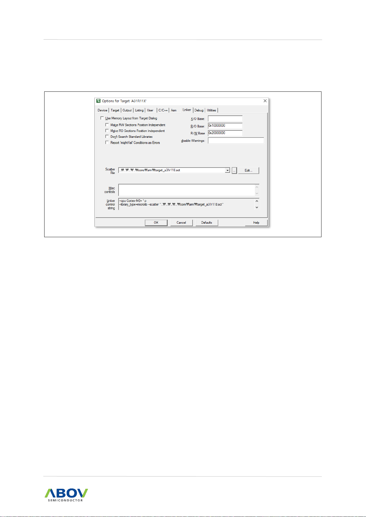
2.1.2 Scatter loading .........................................................................................................7
2.2 Downloading firmware ..........................................................................................................8
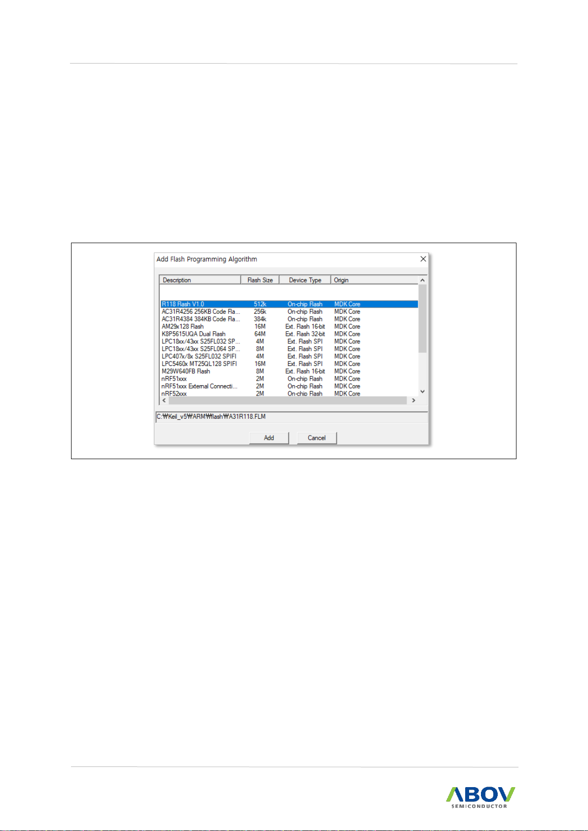
2.2.1 Downloading with Keil ..............................................................................................8
2.2.2 Downloading with drag and drop............................................................................11
2.3 Running application from RAM ...........................................................................................11
3aBLE EVK hardware ....................................................................................................................14
3.1 Block diagram .....................................................................................................................14
3.2 Power supply.......................................................................................................................14
3.3 Connector interface.............................................................................................................15
3.4 Buttons and LEDs ...............................................................................................................16
3.5 Low power crystal ...............................................................................................................16
3.6 Interface MCU .....................................................................................................................17
3.7 Debugger connector (optional) ...........................................................................................17
4Evaluation aBLE EVK ..................................................................................................................18
4.1 Current measurement .........................................................................................................18
4.2 RF measurement ................................................................................................................18
Revision history .....................................................................................................................................20

aBLE EVK application note List of figures
3
List of figures
Figure 1. C Pre-processor.......................................................................................................................6
Figure 2. Scatter Loading........................................................................................................................7
Figure 3. Debugger Set...........................................................................................................................8
Figure 4. Read Device ID........................................................................................................................9
Figure 5. Select Algorithm .....................................................................................................................10
Figure 6. Select Download ....................................................................................................................11
Figure 7. Scatter File Loading ...............................................................................................................12
Figure 8. Set External Tool....................................................................................................................12
Figure 9. Set .ini File .............................................................................................................................13
Figure 10. Keil Specific Debugger Script “boot_from_ram.ini”..............................................................13
Figure 11. aBLE EVK Block Diagram....................................................................................................14
Figure 12. Power Supply.......................................................................................................................14
Figure 13. Power Supply Schematic .....................................................................................................15
Figure 14. Connector Interface .............................................................................................................15
Figure 15. Buttons and LEDs ................................................................................................................16
Figure 16. Low Power Crystal of 32.768KHz ........................................................................................16
Figure 17. Debugger Connector ...........................................................................................................17
Figure 18. Current Measure ..................................................................................................................18
Figure 19. RF Test.................................................................................................................................19

1. Overview aBLE EVK application note
4
1 Overview
The aBLE EVK mounts an aBLE chip (A31R118), to evaluate its performance. The aBLE EVK can be
used as a prototype development board too.
This development kit board has the following key features:
BLE SOC
Buttons and LEDs for user interface
I/O interface for Arduino Shield Compatible plug-in module modules
CMSIS-DAP compatible debug port with
—Virtual COM Port interface via UART
—Drag and Drop Mass Storage Device(MSD) programming
Requirements for hardware and software before enabling the aBLE EVK are listed below:
Hardware
—aBLE Evaluation Board Kit (EVK)
—Arduino plug-in modules (optional)
Software
—aBLE SDK
—Toolchain, any of
▪Keil uVision (Preferred)
▪GNU GCC
▪IAR Embedded Workbench
Document
—Datasheet for aBLE
—aBLE EVK User Guide (this document)
—aBLE EVK hardware files
—aBLE Application Notes

aBLE EVK application note 2. Getting started
5
2 Getting started
aBLE SDK contains many examples for the MCU peripherals and the BLE applications. In following
sections, general processes of building, loading, and running a BLE application on the EVK are
described. Any toolchains can be used to build examples for each process, and Keil uVision is used in
this document.
For A31R118 EVK, refer to following sections:
Section 2.1 Building firmware
Section 2.2 Downloading the firmware
Section 2.3 running application from RAM space
2.1 Building firmware
The general process of building firmware is shown below:
1. Download and install Keil uVision (Lite version is sufficient for all examples).
2. Select an example to build in the example folder.
3. Double click on the example project file (*.uvprojx).
4. Modify chip specific settings (preprocessor and scatter loading file).
5. Click on a button “Build” or “Rebuild”.

aBLE EVK application note 2. Getting started
7
2.1.2 Scatter loading
The scatter loading file for BLE applications must be set properly as shown in Figure 2 (example of
A31R118).
●For A31R118, use target_a31r118.sct
Figure 2. Scatter Loading
To run the application of RAM, use target_a311x_ram.sct (refer to section 2.3).

2. Getting started aBLE EVK application note
8
2.2 Downloading firmware
Once the build of example application is complete successfully, the firmware can be downloaded onto
the EVK by using one of the two different methods:
Method 1. Keil’s download feature
Method 2. Drag and drop.
2.2.1 Downloading with Keil
1. Select the CMSIS-DAP debugger from the debugger selection menu.
Figure 3. Debugger Set

aBLE EVK application note 2. Getting started
9
2. Make sure that the debugger settings and connections are proper by checking the SW device
ID.
Figure 4. Read Device ID
3. Copy the flash download algorithm files provided in the SDK to the Keil’s flash directory.
—aBLE flash algorithm files: “<aBLE SDK Root>\flash\*.flm”
—Keil’s flash directory: “<Keil install root>\ARM\Flash\”
▪Typically, the flash download algorithm files are located at “C:\Keil_v5\ARM\Flash”.

2. Getting started aBLE EVK application note
10
4. Select a desired algorithm from the debugger’s menu
—[Project] menu
—[Options for Target A31R11X]
—[Debug] tab
—[Settings] button
—[Flash Download]
—[Add] button
—Select the proper file according to the chip used.
Figure 5. Select Algorithm

aBLE EVK application note 2. Getting started
11
5. From [Flash] menu, select [Download].
Figure 6. Select Download
2.2.2 Downloading with drag and drop
Another method- to download the application is to use Drag and Drop feature of the interface MCU.
When the EVK is connected and the corresponding drivers are installed correctly, there should be a
new disk drive named “DAPLINK”. The built-binary files (either raw binary format having .bin extension
or intel HEX format having .hex extension) can be copied to this USB drive.
Once it is copied, the interface MCU will flash the internal aBLE programming area, and will reset the
aBLE chip.
2.3 Running application from RAM
It is also possible to run an application from the RAM area. Applications for A31R118 can be executed
without altering the already programmed-flash memory.
There are size limits as some of RAM area is used for executing the code, but it is faster since there is
no download process.
To run applications from RAM, please follow the procedure below:
1. Build application with Scatter Loading file for RAM execution.
2. Set Keil not to download the firmware during debugging.
3. Use Debugger script to load and start the application from RAM.

2. Getting started aBLE EVK application note
12
The application itself must be built for RAM execution. To achieve this, use the provided scatter loading
file for RAM execution.
Figure 7. Scatter File Loading
Set Keil not to download firmware to the flash by choosing external tool option.
Figure 8. Set External Tool

aBLE EVK application note 2. Getting started
13
Use the provided debugger script to load the application and start it.
Figure 9. Set .ini File
The “boot_from_ram.ini” file is a Keil specific debugger script, which instructs Keil to load and start the
application from RAM space. The script contains the code shown in Figure 10.
SP = _RDWORD(0x20000000);
/* Set the stack pointer */
PC = _RDWORD(0x20000004);
/* Set the program counter */
_WDWORD(0xE000ED08, 0x20000000);
/* Set Vector Table Offset to use */
xPSR=0xF1000000;
Figure 10. Keil Specific Debugger Script “boot_from_ram.ini”
At this point, pressing the “Start Debug Session” button runs the script to operate the application.

3. aBLE EVK hardware aBLE EVK application note
14
3 aBLE EVK hardware
The able EVK can be used as a development platform for the aBLE chip. It features an on-board
programming and debugging solution. In addition, aBLE device operates BLE RF and communicates
with a PC over virtual COM port provided by the interface MCU.
3.1 Block diagram
Figure 11 shows the block diagram of the aBLE EVK.
Figure 11. aBLE EVK Block Diagram
3.2 Power supply
The aBLE EVK board provides three power options as shown below:
USB
External Power
Coin Cell Battery
Figure 12. Power Supply

aBLE EVK application note 3. aBLE EVK hardware
15
Figure 13 shows the schematic for power options.
Figure 13. Power Supply Schematic
3.3 Connector interface
In addition to the power and ground, every available PIN to aBLE MCU is routed to the connector. Figure
14 shows the connector interface on the board.
Figure 14. Connector Interface

3. aBLE EVK hardware aBLE EVK application note
16
3.4 Buttons and LEDs
Two buttons and two LEDs in red squares of Figure 15 are connected to I/Os on the EVK board. The
buttons and LEDs can be disconnected so that IOs are used for other purposes.
To measure current, the LEDs must be disconnected.
Figure 15. Buttons and LEDs
3.5 Low power crystal
A 32.768KHz crystal (X2) is available for the aBLE series as an option. This is especially needed when
software is programmed for system sleep since the external crystal provides better accuracy over
internal RC oscillator.
Figure 16 shows 32.768KHz crystal’s schematic and PCB.
Figure 16. Low Power Crystal of 32.768KHz

aBLE EVK application note 3. aBLE EVK hardware
17
3.6 Interface MCU
The aBLE EVK has a reset/boot button on it. This button is connected to the interface MCU and has
two functions listed below:
It acts as a reset button for the aBLE device (via software reset).
It enters the aBLE EVK in bootloader mode of the interface MCU
During normal operation, pressing the button will cause a reset to the connected aBLE MCU. Power
cycling through the board (either by using the power switch or by reconnecting the USB cable while the
power switch is on position) with the button pressed causes the interface MCU to enter into the
bootloader mode so that the interface MCU itself can be updated.
When releasing the EVK, the proper interface MCU firmware is already flashed according to the
corresponding aBLE chip mounted on the EVK.
In addition, the interface MCU provides a function of CMSIS-DAP debugger interface. When connected
to a PC, corresponding software driver should be installed automatically. The debugger must be
selected accordingly from the IDE to be used.
The interface MCU provides a Virtual COM port via UART. Since the Virtual COM port is connected to
the default UART0 pins of the aBLE MCU, the standard “printf” style input or output can be used during
debugging process.
3.7 Debugger connector (optional)
Debugger connector allows users to connect over SWD while battery or external power supply is used.
To do so, the switch for routing SWCLK and SWDIO must be set to external connectors.
Figure 17. Debugger Connector

4. Evaluation aBLE EVK aBLE EVK application note
18
4 Evaluation aBLE EVK
4.1 Current measurement
Current drawn by the aBLE device can be monitored on the aBLE EVK board. To measure the current,
a user can remove P2 short header and connect ampere-meter between the pins of connector P2. By
doing this, the user can monitor the current directly.
Figure 18 shows schematic and current monitor pin on the PCB.
Figure 18. Current Measure
4.2 RF measurement
The aBLE EVK board is equipped with a small size coaxial connector for conducted measurements of
the RF signal (E1). This is a Murata’s SWF type connector (part no. MM8430-2610RA1) with an internal
switch. By default, when there is no cable attached, the RF signal is routed to the on-board Planar
Inverted-F antenna (PIFA Antenna).
A test probe is available at Murata (part no. MXHS83QE3000), which has a standard SMA connection
on the other end to connect instruments. When connecting the test probe, the internal switch in the
SWF connector will disconnect the PCB antenna and connect the RF signal from the aBLE device to
the test probe. Figure 19 shows schematic and the RF port on the PCB.

aBLE EVK application note 4. Evaluation aBLE EVK
19
Figure 19. RF Test
To verify the RF performance, a user can use Direct Test Mode (DTM). Since the aBLE supports UART
mode, the user can test in the DTM by using HCIC firmware which is one of examples provided in SDK.
PB2 (RXD) and PB3 (TXD) will be used to connect to the test probes.

Revision history aBLE EVK application note
20
Revision history
Version
Date
Revision list
2.10
2017.11.30
Initial version created
2.20
2018.03.06
2.30
2019.05.22
2.40
2020.02.18
Revised typo and ambiguous words
2.50
2020.07.22
Revised typo and ambiguous words
2.60
2022.10.31
Changed the font
Table of contents
Other Abov Motherboard manuals