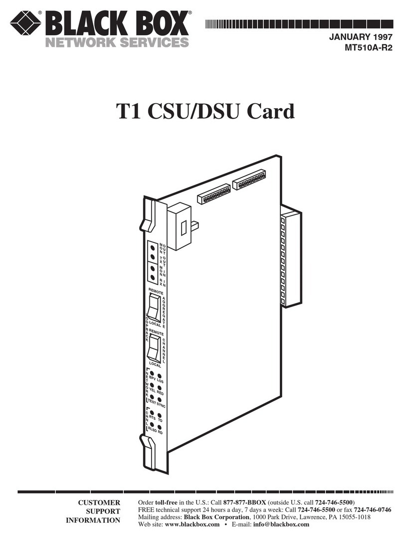
Acromag AVME9440 Series User manual

-~
ARTISAN
®
~I
TECHNOLOGY
GROUP
Your definitive source
for
quality
pre-owned
equipment.
Artisan Technology
Group
Full-service,
independent
repair
center
with
experienced
engineers
and
technicians
on staff.
We
buy
your
excess,
underutilized,
and
idle
equipment
along
with
credit
for
buybacks
and
trade-ins
.
Custom
engineering
so
your
equipment
works
exactly as
you
specify.
•
Critical
and
expedited
services
•
Leasing
/
Rentals/
Demos
• In
stock/
Ready-to-ship
•
!TAR-certified
secure
asset
solutions
Expert
team
ITrust
guarantee
I
100%
satisfaction
All
tr
ademarks,
br
a
nd
names, a
nd
br
a
nd
s a
pp
earing here
in
are
th
e property of
th
e
ir
r
es
pecti
ve
ow
ner
s.
Find the Acromag / Xembedded / Xycom AVME9440-I-L at our website: Click HERE


AVME9440/9443/9447 ISOLATED DIGITAL I/O BOARDS
____________________________________________________________________________
- 1 -
The information in this manual is subject to change without notice. Acromag, Inc., makes no warranty
of any kind with regard to this material, including, but not limited to, the implied warranties of
merchantability and fitness for a particular purpose. Further, Acromag, Inc., assumes no
responsibility for any errors that may appear in this manual and makes no commitment to update, nor
keep current, the information contained in this manual.
No part of this manual may be copied or reproduced in any form, or by any means, without the prior
written consent of Acromag, Inc.
IMPORTANT SAFETY CONSIDERATIONS
It is very important for the user to consider the possible adverse effects of power, wiring, component,
sensor or software failures in designing any type of control or monitoring system. This is especially
important where economic property loss or human life is involved. It is important that the user employ
redundancy, and comprehensive failure analysis to insure a safe and satisfactory overall system
design. It is agreed between the Buyer and Acromag, that this is the Buyer's responsibility.
ACROMAG, INCORPORATED Tel: (248) 624-1541
30765 South Wixom Road Fax: (248) 624-9234
PO Box 437
Wixom, MI 48393-7037, USA
Copyright 1992, 1995 Acromag, Inc. Printed in USA
Data and specifications subject to change without notice

AVME9440/9443/9447 ISOLATED DIGITAL I/O BOARDS
___________________________________________________________________________
- 2 -
TABLE OF CONTENTS
CHAPTER
Page
1.0 GENERAL INFORMATION...................................................................................................... 4
1.1 INTRODUCTION...................................................................................................................... 4
1.2 DIGITAL INPUT FEATURES ( 9440-I & 9447-I )...................................................................... 4
1.3 DIGITAL OUTPUT FEATURES ( 9440-I & 9443-I ).................................................................. 4
1.4 VMEbus INTERFACE FEATURES........................................................................................... 5
1.5 FIELD COMPATIBILITY........................................................................................................... 5
1.5.1 Digital Inputs..................................................................................................................... 5
1.5.2 Digital Outputs.................................................................................................................. 5
2.0 PREPARATION FOR USE....................................................................................................... 5
2.1 UNPACKING AND INSPECTION............................................................................................. 5
2.2 CARD CAGE CONSIDERATIONS........................................................................................... 6
2.3 BOARD CONFIGURATION...................................................................................................... 6
2.3.1 Default Jumper Configuration........................................................................................... 6
2.3.1.1 Digital Input Default Configuration.......................................................................... 6
2.3.1.2 Digital Output Default Configuration....................................................................... 6
2.4 VMEbus CONFIGURATION.................................................................................................... 7
2.4.1 Address Decode Jumper Configuration........................................................................... 7
2.4.2 Address Modifier Jumper Configuration........................................................................... 8
2.4.3 Interrupt Level Select Jumper Configuration.................................................................... 8
2.5 DIGITAL INPUT CONFIGURATION ( 9440-I & 9447-I ) ......................................................... 8
2.5.1 Digital Input Threshold Detection..................................................................................... 9
2.5.2 Sensing Contact Closures and Switches......................................................................... 9
2.5.3 Debounce Delay Selection............................................................................................... 9
2.6 DIGITAL OUTPUT CONFIGURATION ( 9440-I & 9443-I ) ..................................................... 9
2.6.1 Relay Coils and Other Inductive Loads............................................................................ 9
2.7 DIGITAL INPUT/OUTPUT INTERFACE TO TTL AND CMOS SIGNALS................................ 10
2.8 CONNECTORS........................................................................................................................ 10
2.8.1 Digital Input Connector..................................................................................................... 10
2.8.2 Digital Output Connector.................................................................................................. 11
2.8.3 VMEbus Connections....................................................................................................... 11
2.9 POWER-UP TIMING AND LOADING...................................................................................... 12
2.10 DATA TRANSFER TIMING..................................................................................................... 13
2.11 FIELD GROUNDING CONSIDERATIONS.............................................................................. 13
3.0 PROGRAMMING INFORMATION........................................................................................... 13
3.1 MEMORY MAP......................................................................................................................... 13
3.1.1 Board Identification PROM............................................................................................... 15
3.1.2 Board Status Register....................................................................................................... 16
3.1.2.1 Status Bits Usage.................................................................................................... 16
3.1.3 Interrupt Vector Registers................................................................................................. 17
3.1.4 Digital Input Channel Interrupt Status Register................................................................. 17
3.1.5 Digital Input Channel Interrupt Enable Register................................................................ 18
3.1.6 Digital Input Channel Interrupt Polarity Register............................................................... 18
3.1.7 Digital Input Channel Interrupt Type Select Register........................................................ 18
3.1.8 Digital Input Channel Interrupt Pattern Enable Register................................................... 19
3.1.9 Digital Input Channel Data Register.................................................................................. 19
3.1.10 Digital Output Channel Data Register.............................................................................. 19
3.2 GENERAL PROGRAMMING CONSIDERATIONS.................................................................. 20
3.2.1 Board Diagnostics............................................................................................................. 20

AVME9440/9443/9447 ISOLATED DIGITAL I/O BOARDS
____________________________________________________________________________
- 3 -
TABLE OF CONTENTS
CHAPTER
Page
3.3 GENERATING INTERRUPTS.................................................................................................. 20
3.3.1 Interrupt Example For Change Of State (COS)................................................................ 21
3.3.2 Interrupt Example For Input Level (Polarity) Match.......................................................... 21
3.3.3 Interrupt Example For Input Pattern Match....................................................................... 22
3.3.4 Sequence of Events For an Interrupt................................................................................ 22
4.0 THEORY OF OPERATION....................................................................................................... 23
4.1 VMEbus INTERFACE............................................................................................................... 23
4.1.1 VMEbus Control Logic...................................................................................................... 23
4.1.2 VME Interrupter................................................................................................................ 23
4.2 REGISTER LOCATION SUMMARY........................................................................................ 24
4.3 ISOLATION BARRIER............................................................................................................. 24
4.4 DIGITAL INPUT SECTION ( 9440-I & 9447-I )......................................................................... 24
4.5 DIGITAL OUTPUT SECTION ( 9440-I & 9443-I )..................................................................... 24
5.0 SERVICE AND REPAIR INFORMATION................................................................................ 25
5.1 SERVICE AND REPAIR ASSISTANCE................................................................................... 25
5.2 PRELIMINARY SERVICE PROCEDURE................................................................................ 25
5.3 PARTS LISTS........................................................................................................................... 25
6.0 SPECIFICATIONS.................................................................................................................... 29
FIGURES:
2.1 AVME944X JUMPER LOCATION DRAWING (4501-130)....................................................... 31
2.2 AVME944X-I-L LED EXPANSION BOARD ASSEMBLY (4501-125)....................................... 32
2.3 AVME944X SIMPLIFIED DIGITAL INPUT POINT SCHEMATIC (4501-131)........................... 33
2.4 AVME944X DIGITAL INPUT POINT CONFIGURATIONS (4501-132).................................... 34
2.5 AVME944X SIMPLIFIED DIGITAL OUTPUT POINT SCHEMATIC (4501-133)....................... 35
2.6 AVME944X DIGITAL OUTPUT POINT CONFIGURATIONS (4501-134)................................ 36
2.7 AVME944X INTERFACE TO TTL AND CMOS SIGNALS (4501-137)..................................... 37
3.3 AVME944X INPUT RESPONSE AND INTERRUPT TIMING DIAGRAM (4501-124).............. 38
4.1 AVME944X BLOCK DIAGRAM (4501-128).............................................................................. 39
AVME944X SCHEMATIC & PART LOCATION DRAWING (4501-129)................................... 40
AVME944X LED EXPANSION BOARD SCH. & PART LOC. DRAWING (4501-136).............. 53
APPENDIX:
A.0 CABLE AND TERMINATION PANELS.................................................................................. 55
A.1 CABLE: MODEL 9944-x.......................................................................................................... 55
A.2 TERMINATION PANELS: MODELS 6985-16DI AND 6985-16DO......................................... 55
9944-X FLAT 64 PIN CABLE (4501-135)........................................................................................ 57
6985-16DX SCHEMATIC & PART LOCATION DRAWING (4501-126).......................................... 58
6985-16DX MOUNTING CLEARANCE & ELECTRICAL CONNECTIONS (4501-127).................. 60

AVME9440/9443/9447 ISOLATED DIGITAL I/O BOARDS
___________________________________________________________________________
- 4 -
1.0 GENERAL INFORMATION
1.1 INTRODUCTION
The AVME944x Series of VME cards offer a variety of features which make them an ideal choice for many
industrial and scientific applications.
MODEL 16 Channel
Digital In 16 Channel
Digital Out Channel On
LEDs
AVME9440-I XX XX
AVME9440-I-L XX XX XX
AVME9443-I XX
AVME9443-I-L XX XX
AVME9447-I XX
AVME9447-I-L XX XX
General Features
•All Digital Inputs and Outputs are optically isolated from the VMEbus and from each other (250 VAC).
•Field connections accessible through connectors mounted on the Front Panel.
•Can be interfaced to TTL & CMOS logic.
•PASS/FAIL status indicator LEDs on the front panel.
•Optional Termination Panels.
1.2 DIGITAL INPUT FEATURES ( 9440-I & 9447-I )
•16 input points configured as a 16 bit word.
•Input range of up to 55 VDC (over 2 selectable ranges).
•Optically-coupled logic gates.
•Adjustable debounce circuitry.
•Generation of interrupts for channels 0 through 7: input Change Of State (COS), input level (polarity) match,
or input pattern detection.
•Input channel ON indicating LEDs (with -L option).
1.3 DIGITAL OUTPUT FEATURES ( 9440-I & 9443-I )
•16 output points configured as a 16 bit word.
•Ability to read back output states (for complete confidence in the output setting, the output should be fed
back to an input point and the input point monitored).
•Outputs sink up to 1 Amp DC, from up to a 55 VDC source.
•Solid State Relays (SSRs) operate as Single Pole, Single Throw (SPST), Form A relays.
•Output channel ON (output switch closed) indicating LEDs (with -L option).

AVME9440/9443/9447 ISOLATED DIGITAL I/O BOARDS
____________________________________________________________________________
- 5 -
1.4 VMEbus INTERFACE FEATURES
•Slave module A24/A16, D16/D08 (EO).
•Short I/O Address Modifiers 29H, 2DH (H = Hex).
•Standard Address Modifiers 39H, 3DH (H = Hex).
•I(1-7) interrupter, jumper programmable interrupt level, software programmable interrupt vectors (for digital
input channels 0-7), interrupt release mechanism is Release On Register Access (RORA) type.
•Decode on 1K byte boundaries.
1.5 FIELD COMPATIBILITY
See APPENDIX A for more information on compatible products.
1.5.1 Digital Inputs
Directly compatible with Acromag input termination panel.
Cable:
Model 9944-X: Flat 64 pin cable (female connectors at both ends) for connecting the AVME944X to the
6985-16DI termination panel.
Termination Panel:
Model 6985-16DI: Sixteen channel input digital termination panel.
1.5.2 Digital Outputs
Directly compatible with Acromag output termination panel.
Cable:
Model 9944-X: Flat 64 pin cable (female connectors at both ends) for connecting the AVME944X to the
6985-16DO termination panel.
Termination Panel:
Model 6985-16DO: Sixteen channel output digital termination panel.
2.0 PREPARATION FOR USE
This chapter provides information about preparing the Isolated Digital I/O Board for system operation.
2.1 UNPACKING AND INSPECTION
Inspect the shipping carton immediately upon receipt for evidence of mishandling during transit. If the shipping
carton is severely damaged or water stained, request that the carrier's agent be present when the carton is
opened. If the carrier's agent is absent when the carton is opened and the contents of the carton are damaged,
keep the carton and packing material for the agent's inspection.

AVME9440/9443/9447 ISOLATED DIGITAL I/O BOARDS
___________________________________________________________________________
- 6 -
For repairs to a product damaged in shipment, refer to the Acromag Service Policy to obtain return instructions.
It is suggested that salvageable shipping cartons and packing material be saved for future use in the event the
product must be shipped.
The board is physically protected with foam and electrically protected with an antistatic bag during shipment. It
is advisable to visually inspect the board for evidence of mishandling prior to applying power.
CAUTION
SENSITIVE ELECTRONIC DEVICES
USE ANTI-STATIC HANDLING PROCEDURES
2.2 CARD CAGE CONSIDERATIONS
Refer to the specifications for bus loading and power requirements. Be sure that the system power supplies are
able to accommodate the additional requirements within the voltage tolerances specified.
Adequate air circulation must be provided to prevent a temperature rise above the maximum operating
temperature. Large and continuing fluctuations in ambient air temperature should be avoided. If the installation
is in an industrial environment and the board is exposed to environmental air, careful consideration should be
given to air filtering.
2.3 BOARD CONFIGURATION
The board may be configured in a variety of ways for many different applications. Each possible jumper setting
will be discussed in the following sections. The jumper locations are shown in Figure 2.1. Note that if you have
a model containing the LED Expansion Board (-L suffix), it must be removed to change the digital input channel
range jumpers (J9-J24). See Figure 2.2 for the LED Expansion Board assembly instructions.
2.3.1 Default Jumper Configuration
VMEbus INTERFACE CONFIGURATION
When a board is shipped from the factory, it is configured as follows:
•VMEbus Short I/O Address of 0000H.
•Set to respond to both Address Modifiers 29H and 2DH.
•Interrupt Level: none. Therefore, even if interrupts are enabled, no interrupts will be caused.
2.3.1.1 Digital Input Default Configuration
•16 dedicated digital input points (numbered 0 through 15).
•All channels factory configured (via jumpers) for the 4-25V DC input range.
•Minimum input debounce selected.
2.3.1.2 Digital Output Default Configuration
•16 dedicated digital output points (numbered 0 through 15).

AVME9440/9443/9447 ISOLATED DIGITAL I/O BOARDS
____________________________________________________________________________
- 7 -
2.4 VMEbus CONFIGURATION
2.4.1 Address Decode Jumper Configuration
The board interfaces with the VMEbus as a 1K block of address locations in the VMEbus Short I/O Address
Space or Standard Address Space. J2 and J1 decode the fourteen most significant address lines A10 through
A23 to provide segments of 1K address space. The configuration of the jumpers for different base address
locations is shown below. "IN" means that the pins are shorted together with a shorting clip. "OUT" indicates
that the clip has been removed. J2 decodes address lines A10 through A15 and J1 decodes Address lines A16
through A23. Therefore, when configured for the Short I/O Address space, only J2 needs to be configured.
Pins of J2
BASE
ADDR
(HEX) A15
(11 & 12) A14
(10 & 9) A13
(8 & 7) A12
(6 & 5) A11
(4 & 3) A10
(2 & 1)
0000 OUT OUT OUT OUT OUT OUT
0400 OUT OUT OUT OUT OUT IN
0800 OUT OUT OUT OUT IN OUT
0C00 OUT OUT OUT OUT IN IN
1000 OUT OUT OUT IN OUT OUT
.......
.......
.......
EC00 IN IN IN OUT IN IN
F000 IN IN IN IN OUT OUT
F400 IN IN IN IN OUT IN
F800 IN IN IN IN IN OUT
FC00 IN IN IN IN IN IN
Pins of J1
BASE
ADDR
(HEX) A23
(15&16) A22
(13&14) A21
(11&12) A20
(9&10) A19
(7&8) A18
(5&6) A17
(3&4) A16
(1&2)
000000 OUT OUT OUT OUT OUT OUT OUT OUT
010000 OUT OUT OUT OUT OUT OUT OUT IN
020000 OUT OUT OUT OUT OUT OUT IN OUT
030000 OUT OUT OUT OUT OUT OUT IN IN
.........
.........
.........
FC0000 IN IN IN IN IN IN OUT OUT
FD0000 IN IN IN IN IN IN OUT IN
FE0000 IN IN IN IN IN IN IN OUT
FF0000 IN IN IN IN IN IN IN IN

AVME9440/9443/9447 ISOLATED DIGITAL I/O BOARDS
___________________________________________________________________________
- 8 -
2.4.2 Address Modifier Jumper Configuration
The VMEbus Address Modifier jumpers (J3, J5, and J6) permit the board to respond to the various Address
Modifier Codes.
Pins of J3,J5,J6
J3
1&2 J3
2&3 J5
1&2 J6
1&2 Address Modifier Code/Function
OUT IN OUT IN 2DH Only Short Supervisory Access
OUT IN IN IN 2DH & 29H Short Supervisory Access
and Short Non-privileged Access
IN OUT OUT OUT 3DH Only Standard Supervisory Data Access
IN OUT IN OUT 3DH & 39H Standard Supervisory Data Access
and Standard Non-privileged Data Access
2.4.3 Interrupt Level Select Jumper Configuration
The board Interrupt Level is selected by configuring jumper J4 as follows:
Interrupt
Level J4
(5&6 ) J4
(3&4) J4
(1&2)
None OUT OUT OUT
1 OUT OUT IN
2 OUT IN OUT
3 OUT IN IN
4 IN OUT OUT
5 IN OUT IN
6 IN IN OUT
7 IN IN IN
2.5 DIGITAL INPUT CONFIGURATION ( 9440-I & 9447-I )
Selectable input threshold voltages make the digital input points adaptable to almost any application. The inputs
are designed for use with contact closures, switches, alarm trips, and power supply ON/OFF monitoring. Input
points are optically isolated from each other and from the VMEbus. See Figure 2.3 for the simplified schematic
of a digital input point.
Input channel debounce circuitry with selectable delay is also provided for each channel to eliminate glitches
from the input signals. These glitches are frequently caused by contact bounce in mechanical relays and
switches.

AVME9440/9443/9447 ISOLATED DIGITAL I/O BOARDS
____________________________________________________________________________
- 9 -
2.5.1 Digital Input Threshold Selection
Two input threshold voltages are selectable on a per channel basis by J9 to J24 to cover the input ranges from 4
to 55V DC, as shown in the following table:
Channel Range J9-J24
1&2 J9-J24
2&3 Positive Threshold
Voltage (Maximum)
4-25V DC OUT IN 4V DC
20-55V DC IN OUT 20V DC
2.5.2 Sensing Contact Closures and Switches
The input voltage should be within the range listed in the previous table. See Figure 2.4: Digital Input Point
Configurations, for connections for different input types.
2.5.3 Debounce Delay Selection
If mechanical relay contacts (or switches) are used as inputs, it is strongly recommended that a debounce delay
longer than the maximum expected bounce time be used. If the bounce time cannot be determined, then the
maximum debounce delay should be selected.
The debounce delay time is jumper programmable (J7) on a global basis for all input channels (i.e. all input
channels will have the same delay), as shown in the following table:
Debounce Delay
Time (uS) J7
1&2 J7
3&4 J7
5&6 J7
7&8
7 to 8 OUT OUT OUT IN
336 to 384 OUT OUT IN OUT
672 to 768 OUT IN OUT OUT
1344 to1536 IN OUT OUT OUT
NOTE: One of the debounce delay times must be selected. If none or more than one delay time is selected, the
input signals will not pass through the debounce circuit.
2.6 DIGITAL OUTPUT CONFIGURATION ( 9440-I & 9443-I )
The Digital Outputs are designed to control valves, switch counters, mechanical relays, optical relays, indicator
lamps, etc. Each digital output can be written to and then read back immediately for verification purposes, but
for complete confidence in the output setting, the output should be fed back to an input point and the input point
monitored. See Figure 2.5 for the simplified schematic of a digital output point. Outputs include reverse bias
protection and a replaceable fuse (requires soldering). Output loads of up to 1 Amp DC and voltages up to 55V
DC are supported.
2.6.1 Relay Coils and Other Inductive Loads
When driving relay coils or other inductive loads, diodes should be placed across each load to limit the voltage
spike generated when an inductive load is switched off quickly. See Figure 2.6: Digital Output Point
Configurations, for connections for different output types.

AVME9440/9443/9447 ISOLATED DIGITAL I/O BOARDS
___________________________________________________________________________
- 10 -
2.7 DIGITAL INPUT/OUTPUT INTERFACE TO TTL AND CMOS SIGNALS
Logic level inputs can be interfaced to the board by the use of common logic elements such as the 74LS05 (or
74HC05) open collector (or drain) inverter gates. See Figure 2.7: Interface to TTL and CMOS Signals, for
connection information. Applying a logic "1" to the input of the inverter gate sinks the current required to turn the
optically-coupled logic gate on (using the lowest input voltage range) and yields a logic "1" for the corresponding
input channel register bit position.
Logic level outputs are easily interfaced by the use of 74LS04 (or 74HC04) inverter gates. Programming a logic
"1" in the corresponding output channel register bit position turns on the output SSR which pulls the input to the
inverter gate low. This yields a logic "1" at the output of the inverter gate.
2.8 CONNECTORS
2.8.1 Digital Input Connector
Digital inputs are connected to the 944x via connector P4 (lower connector as viewed from the front). Table 2.1
defines the assignment. These connections are easily accommodated through the use of Acromag termination
panels and flat cable assemblies or through the use of a user defined termination panel.
P4: Panduit No. 100-532-053; Series 100, Type B Male Connectors, rows A & B equipped, even pins only (32
pins total).
Table 2.1: P4 CONNECTOR
Pin Number Mnemonic Pin Number Mnemonic
32A CH0+ 32B CH0-
30A CH1+ 30B CH1-
28A CH2+ 28B CH2-
26A CH3+ 26B CH3-
24A CH4+ 24B CH4-
22A CH5+ 22B CH5-
20A CH6+ 20B CH6-
18A CH7+ 18B CH7-
16A CH8+ 16B CH8-
14A CH9+ 14B CH9-
12A CH10+ 12B CH10-
10A CH11+ 10B CH11-
8A CH12+ 8B CH12-
6A CH13+ 6B CH13-
4A CH14+ 4B CH14-
2A CH15+ 2B CH15-

AVME9440/9443/9447 ISOLATED DIGITAL I/O BOARDS
____________________________________________________________________________
- 11 -
2.8.2 Digital Output Connector
Digital outputs are connected to the 944x via connector P3 (upper connector as viewed from the front). Table
2.2 defines the assignment. These connections are easily accommodated through the use of Acromag
termination panels and flat cable assemblies or through the use of a user defined termination panel.
P3: Panduit No. 100-532-053; Series 100, Type B Male Connectors, rows A & B equipped, even pins only (32
pins total).
Table 2.2: P3 CONNECTOR
Pin Number Mnemonic Pin Number Mnemonic
32A CH0+ 32B CH0-
30A CH1+ 30B CH1-
28A CH2+ 28B CH2-
26A CH3+ 26B CH3-
24A CH4+ 24B CH4-
22A CH5+ 22B CH5-
20A CH6+ 20B CH6-
18A CH7+ 18B CH7-
16A CH8+ 16B CH8-
14A CH9+ 14B CH9-
12A CH10+ 12B CH10-
10A CH11+ 10B CH11-
8A CH12+ 8B CH12-
6A CH13+ 6B CH13-
4A CH14+ 4B CH14-
2A CH15+ 2B CH15-
2.8.3 VMEbus Connections
Table 2.3 indicates pin assignments for the VMEbus signals at the P1 connector. The P1 connector is the upper
connector on the 944x board as viewed from the front. The connector consists of 32 rows of three pins labeled
A, B, and C. Pin A1 is located at the upper left hand corner of the connector.

AVME9440/9443/9447 ISOLATED DIGITAL I/O BOARDS
___________________________________________________________________________
- 12 -
TABLE 2.3: P1 BUS CONNECTIONS
PIN NUMBER
MNEMONIC PIN NUMBER
MNEMONIC PIN NUMBER
MNEMONIC
1A D00 1B BBSY* 1C D08
2A D01 2B BCLR * 2C D09
3A D02 3B ACFAIL* 3C D10
4A D03 4B BG0IN* 4C D11
5A D04 5B BG0OUT* 5C D12
6A D05 6B BG1IN* 6C D13
7A D06 7B BG1OUT* 7C D14
8A D07 8B BG2IN* 8C D15
9A GND 9B BG2OUT* 9C GND
10A SYSCLK 10B BG3IN* 10C SYSFAIL*
11A GND 11B BG3OUT* 11C BERR*
12A DS1* 12B BR0* 12C SYSRESET*
13A DS0* 13B BR1* 13C LWORD*
14A WRITE* 14B BR2* 14C AM5
15A GND 15B BR3* 15C A23
16A DTACK* 16B AM0 16C A22
17A GND 17B AM1 17C A21
18A AS* 18B AM2 18C A20
19A GND 19B AM3 19C A19
20A IACK* 20B GND 20C A18
21A IACKIN* 21B SERCLK 21C A17
22A IACKOUT* 22B SERDAT* 22C A16
23A AM4 23B GND 23C A15
24A A07 24B IRQ7* 24C A14
25A A06 25B IRQ6* 25C A13
26A A05 26B IRQ5* 26C A12
27A A04 27B IRQ4* 27C A11
28A A03 28B IRQ3* 28C A10
29A A02 29B IRQ2* 29C A09
30A A01 30B IRQ1* 30C A08
31A -12V 31B +5V STDBY 31C +12V
32A +5V 32B +5V 32C +5V
* Indicates that the signal is active low.
Refer to the VMEbus specification for additional information on the VMEbus signals.
2.9 POWER-UP TIMING AND LOADING
The 944x board uses a Logic Cell Array to handle the bus interface and control logic timing. Upon power-up, the
Logic Cell Array automatically clocks in configuration vectors from a local PROM to initialize the logic circuitry
for normal operation. This time is measured as the first 145 mS (typical) after the +5 Volt supply raises to +2.5
Volts at power-up. If a data transfer is attempted during this time, it will simply be ignored and the board will not
respond. This should not be a problem because the VME specification requires that the bus master drive the
system reset for the first 200 mS after power-up, thus inhibiting any data transfers from taking place.

AVME9440/9443/9447 ISOLATED DIGITAL I/O BOARDS
____________________________________________________________________________
- 13 -
Digital input and output channels are reset to the OFF state following a power-up sequence. External input
signals above threshold levels can then drive inputs ON. Likewise, writing to the digital output registers can
program outputs ON.
2.10 DATA TRANSFER TIMING
Data transfer time is measured from the falling edge of DSx* to the falling edge of DTACK* during a normal data
transfer cycle.
REGISTER DATA TRANSFER TIME
All Registers 580nS, typical
2.11 FIELD GROUNDING CONSIDERATIONS
The board is designed to isolate every input and output channel from each other as well as from the VMEbus.
This is intended to protect each channel and the VMEbus from voltage spikes and transients such as those
caused by ground currents and "pick-up". The isolation provides the ability to earth ground the field wiring
without the concern of ground currents damaging the card cage electronics.
3.0 PROGRAMMING INFORMATION
This chapter provides the specific information necessary to operate the Isolated Digital I/O Board.
3.1 MEMORY MAP
The board is addressable on 1K byte boundaries in the Short I/O Address Space or Standard Address Space. All
Acromag VMEbus non-intelligent slaves have a standard interface configuration which consists of a 32 byte
board ID PROM and a Board Status register. The rest of the 1K byte address space contains registers or
memory specific to the function of the board. The memory map is shown in Figure 3.1 (Addresses in Hex).

AVME9440/9443/9447 ISOLATED DIGITAL I/O BOARDS
___________________________________________________________________________
- 14 -
Figure 3.1: Board Memory Map
Address
Base +
(HEX) D15 Even
D8 D7 Odd
D0
Address
Base +
(HEX)
00
↓
3E Undefined R - Board ID PROM 01
↓
3F
40
↓
7E Undefined Undefined 41
↓
7F
80 Undefined R/W - Board Status 81
82
↓
9E Undefined Undefined 83
↓
9F
A0 Undefined R/W - Int. Vector CH0 A1
A2 " R/W - Int. Vector CH1 A3
A4 " R/W - Int. Vector CH2 A5
A6 Undefined R/W - Int. Vector CH3 A7
A8 " R/W - Int. Vector CH4 A9
AA " R/W - Int. Vector CH5 AB
AC " R/W - Int. Vector CH6 AD
AE " R/W - Int. Vector CH7 AF
B0
↓
BE Undefined Undefined B1
↓
BF
C0 Undefined R/W - Digital Input Channel
Interrupt Status Register
CH7 CH0 C1
C2 Undefined R/W - Digital Input Channel
Interrupt Enable Register
CH7 CH0 C3
C4 Undefined R/W - Digital Input Channel
Interrupt Polarity Register
CH7 CH0 C5
C6 Undefined R/W - Digital Input Channel
Interrupt Type Select
Register
CH7 CH0 C7
C8 Undefined R/W - Digital Input Channel
Int. Pattern Enable Register
CH7 CH0 C9
CA R - Digital Input Channel Data Register
CH15
CH0 CB
CC R/W - Digital Output Channel Data Register
CH15
CH0 CD
CE
↓
3EF Undefined Undefined CF
↓
3FF

AVME9440/9443/9447 ISOLATED DIGITAL I/O BOARDS
____________________________________________________________________________
- 15 -
3.1.1 Board Identification PROM - (read only) - 01H through 3FH (odd)
The board contains an identification section. This section of data describes the board model number and the
manufacturer. The identification section starts at the board's base address plus 1 and is 32 bytes in length.
Bytes are addressed using only the odd addresses between 1 and 63. The PROM contents are shown in Figure
3.2 for an AVME9440-I-L (each model has a unique PROM).
Figure 3.2: AVME9440-I-L Board Identification PROM
Offset Value Descriptions
From Board
Base Address ASCII
Character Numeric
01H V 56H All boards have "VMEID"
03H M 4DH
05H E 45H
07H I 49H
09H D 44H
0BH A 41H Manufacturer's I.D., "ACR" for
0DH C 43H Acromag
0FH R 52H
11H 9 39H Board Model Number (6 characters
13H 4 34H and 1 trailing "blank")
15H 4 34H
17H 0 30H (Each model has a unique number)
19H I 49H
1BH L 4CH
1DH 20H
1FH 1 31H Number of KILOBYTES of address
space used.
21H 20H
23H Undefined Reserved
25H " "
27H " "
29H " "
2BH " "
2DH " "
2FH " "
31H " "
33H " "
35H " "
37H " "
39H " "
3BH " "
3DH " "
3FH Undefined Reserved

AVME9440/9443/9447 ISOLATED DIGITAL I/O BOARDS
___________________________________________________________________________
- 16 -
3.1.2 Board Status Register - (read/write) - 81H
The Board Status Register reflects and controls functions globally on the board.
MSB LSB
7 6 5 4 3 2 1 0
-------------------------------------------------------------------------------------------------------------
<------ Reserved ------> Software Global Global Green Red
Reset Int. Int. LED LED
Enable Pending
Where:
Bits 7,6,5: Reserved for future use - equal "0" if read.
Bit 4: Software Reset (W) - writing a "1" to this bit causes a software reset. Writing "0" or reading the bit has no
effect. The effect of a software reset on the various registers is described in the description of each
register.
Reset Condition: Set to "0".
Bit 3: Global Interrupt Enable (R/W) - writing a "1" to this bit enables interrupts to be serviced, provided the
interrupt level (IRQx*) is selected. A "0" disables servicing interrupts.
Reset Condition: Set to "0", interrupts disabled.
Bit 2: Global Interrupt Pending (R) - this bit will be a "1" when there is an interrupt pending. This bit will be "0"
when there is no interrupt pending. Polling this bit will reflect the board's pending interrupt status, even if
the Global Interrupt Enable bit is set to "0".
Reset condition: Set to "0".
Bit 1: Green LED (R/W) - when written, this bit will control the state of the green LED on the front panel. A "1"
will turn it on, a "0" will turn it off. Reading it will reflect its current state.
Reset Condition: Set to "0", green LED off.
Bit 0: Red LED (R/W) - when written, this bit will control the state of the red LED on the front panel and the state
of the VMEbus SYSFAIL* signal. A "1" will turn the LED off and set SYSFAIL* high, a "0" will turn the
LED on and set SYSFAIL* low. Reading it will reflect its current state. (See Section 5.2 for additional
information on using SYSFAIL*.)
Reset Condition: Set to "0", red LED lit, and SYSFAIL* is set low.
3.1.2.1 Status Bits Usage
The status register bits 1 and 0 along with the green and red LEDs provide the user with a means of keeping
track of a board's functionality in the system. Since there is no intelligence on the board, the host computer
controls these bits. The following paragraphs and summary table describe possible uses of the bits in the status
register and the LEDs on the front panel.
On power-up the bits in the status register read low, with the green LED off, the red LED lit, and SYSFAIL* low.
This indicates that the board has failed or that it has not been tested yet.
If the status register bit 1 reads low and Bit 0 reads high, the LEDs will both be off and SYSFAIL* high. This
indicates an inactive board.

AVME9440/9443/9447 ISOLATED DIGITAL I/O BOARDS
____________________________________________________________________________
- 17 -
If the status register bit 1 reads high and Bit 0 reads low, the LEDs will both be lit and SYSFAIL* low. This
indicates the board is undergoing a diagnostic checkout.
If the status register bits 1 and 0 read high, the green LED will be lit with the red LED off and SYSFAIL* high.
This indicates the board is fully functional.
Status Bits - Possible Usage
Bit 0 Bit 1
(Red LED) (Green LED) SYSFAIL* Description
0, (on) 0, (off) Low Failed or reset condition
1, (off) 0, (off) High Inactive board
0, (on) 1, (on) Low Diagnostics are running
1, (off) 1, (on) High Normal operation
3.1.3 Interrupt Vector Registers - (read/write) - A1H to AFH (Odd addresses)
The interrupt vector registers maintain the 8 bit interrupt vector numbers for each of the 8 digital input channel
interrupt lines. Note that interrupts can only be generated for digital input channels 0-7. The appropriate vector
is provided to the VMEbus Interrupt Handler when an interrupt is being serviced. This allows each digital input
channel interrupt to be serviced by its own software handler. If desired, a single handler can be used by making
all of the vectors the same. In this case, the handler will have to determine the interrupting channel by
examining the interrupt status register.
The register content is undefined upon reset.
3.1.4 Digital Input Channel Interrupt Status Register (read/write) - C1H
The digital input channel interrupt status register reflects the status of the 8 input channels (ch. 0-7). A "1" in a
bit position indicates an interrupt is pending for the corresponding channel. Each bit is derived from the logical
AND of its associated interrupt input and enable bits. Hence, an input channel that does not have interrupts
enabled cannot have its interrupt pending bit set to a "1".
An individual channel's interrupt can be cleared by writing a "1" to its bit position in the interrupt status register.
However, if the condition which caused the interrupt remains or reappears, a new interrupt will be generated. To
permanently disable a channel's interrupt, the corresponding bit in the channel interrupt enable register must be
cleared, followed by writing a "1" to the channel's bit position in the channel interrupt status register (to clear the
interrupt). This is known as the "Release On Register Access" (RORA) method as defined in the VME system
architecture.
Bit 7 of this register has a dual purpose. In addition to indicating an interrupt for channel 7, it is also used to
indicate an input channel bit pattern match (see the digital input channel interrupt pattern enable register).
MSB LSB
7 6 5 4 3 2 1 0
---------------------------------------------------------------------------------------------------
CH7 CH6 CH5 CH4 CH3 CH2 CH1 CH0
All interrupts are cleared following a reset.
NOTE: Interrupts are prioritized via hardware within the card. Channel 7 is the highest priority and channel 0 is
the lowest. If multiple input channel interrupts become pending simultaneously, the vector corresponding to the

AVME9440/9443/9447 ISOLATED DIGITAL I/O BOARDS
___________________________________________________________________________
- 18 -
highest numbered channel will be delivered first. After the highest channel's interrupt is serviced and cleared, an
additional interrupt will be generated for the next highest priority interrupt (pending) channel.
NOTE: Input channel bandwidth should be limited to reduce the possibility of missing channel interrupts. For a
specific input channel this could happen if multiple changes occur before the channel's interrupt is serviced.
3.1.5 Digital Input Channel Interrupt Enable Register (read/write) - C3H
The digital input channel interrupt enable register provides a mask bit for each of the 8 input channels (ch. 0-7).
A "0" in a bit position will prevent the corresponding input channel from causing an external interrupt. A "1" will
allow the input channel to cause an interrupt (providing that the global interrupt enable bit is set).
MSB LSB
7 6 5 4 3 2 1 0
---------------------------------------------------------------------------------------------------
CH7 CH6 CH5 CH4 CH3 CH2 CH1 CH0
All input channel interrupts are masked ("0") following a reset.
3.1.6 Digital Input Channel Interrupt Polarity Register (read/write) - C5H
The digital input channel interrupt polarity register determines the level that will cause a channel interrupt for
each of the 8 input channels (ch. 0-7). A "0" in a bit position means an interrupt will occur when the input
channel is below threshold (i.e. a "0" in the digital input channel data register). A "1" in a bit position means an
interrupt will occur when the input channel is above threshold (i.e. a "1" in the digital input channel data register).
Note that interrupts will not occur unless they are enabled. The interrupt polarity register will have no effect if
Change Of State (COS) interrupts are selected (see the digital input channel interrupt type select register).
MSB LSB
7 6 5 4 3 2 1 0
---------------------------------------------------------------------------------------------------
CH7 CH6 CH5 CH4 CH3 CH2 CH1 CH0
All bits are set to "0" following a reset which means that the inputs will cause interrupts when they are below
threshold.
3.1.7 Digital Input Channel Interrupt Type Select Register (read/write) - C7H
The digital input channel interrupt type select register determines the type of input channel behavior that will
cause a channel interrupt for each of the 8 input channels (ch. 0-7). A "0" in a bit position means an interrupt will
be generated when the input channel level specified by the digital input channel interrupt polarity register occurs.
A "1" in a bit position means an interrupt will occur when a Change Of State (COS) occurs at the input channel
(either low to high, or high to low).
This manual suits for next models
8
Table of contents
Other Acromag Computer Hardware manuals
Acromag
Acromag XMC610 Series User manual

Acromag
Acromag BusWorks XT Series User manual
Acromag
Acromag XMC630 Series User manual
Acromag
Acromag IOS-7200 User manual

Acromag
Acromag APCe7012E-LF User manual

Acromag
Acromag ACPS3320 User manual

Acromag
Acromag APCe8775 User manual

Acromag
Acromag APCe8675 User manual

Acromag
Acromag XVME-6700 User manual

Acromag
Acromag XVPX-6300 User manual
