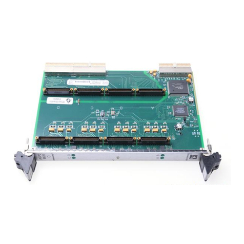
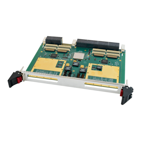
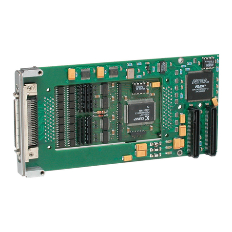
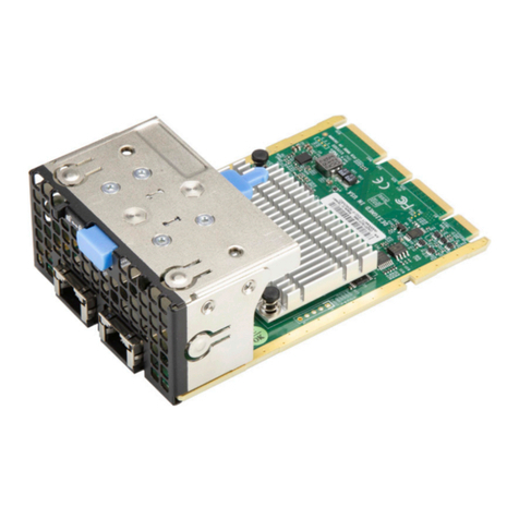
Acromag PMC470 Series User manual

Series PMC470 PCI Mezzanine Card
48-Channel Digital I/O Module With Interrupts
USER’S MANUAL
ACROMAG INCORPORATED
30765 South Wixom Road
P.O. BOX 437
Wixom, MI 48393-7037 U.S.A.
Tel: (248) 624-1541
Fax: (248) 624-9234
Copyright 2000, Acromag, Inc., Printed in the USA.
Data and specifications are subject to change without notice.
8500-674-C05A002
retired

SERIES PMC470 PCI MEZZANINE CARD 48-CHANNEL DIGITAL I/O MODULE WITH INTERRUPTS
___________________________________________________________________________________________
- 2 -
The information contained in this manual is subject to change
without notice. Acromag, Inc. makes no warranty of any kind with
regard to this material, including, but not limited to, the implied
warranties of merchantability and fitness for a particular purpose.
Further, Acromag, Inc. assumes no responsibility for any errors that
may appear in this manual and makes no commitment to update, or
keep current, the information contained in this manual. No part of
this manual may be copied or reproduced in any form, without the
prior written consent of Acromag, Inc.
Table of Contents Page
1.0 GENERAL INFORMATION............................................... 2
KEY PMC470 FEATURES................................................ 2
PCI MEZZANINE CARD INTERFACE FEATURES......... 3
SIGNAL INTERFACE PRODUCTS.................................. 3
PMC MODULE ActiveX CONTROL SOFTWARE............ 3
PMC MODULE VxWORKS SOFTWARE……….............. 3
2.0 PREPARATION FOR USE................................................ 3
UNPACKING AND INSPECTION..................................... 3
CARD CAGE CONSIDERATIONS................................... 3
BOARD CONFIGURATION.............................................. 3
CONNECTORS................................................................. 4
Front Panel Field I/O Connector P1............................... 4
I/O Noise and Grounding Considerations....................... 4
PCI Local Bus Connector ........................………........... 4
3.0 PROGRAMMING INFORMATION.................................... 5
PCI CONFIGURATION ADDRESS SPACE……...……... 5
CONFIGURATION REGISTERS……………...………….. 5
MEMORY MAP….............................................................. 6
Standard (Default) Mode Memory Map........................... 6
Enhanced Mode Memory Map........................................ 7
REGISTER DEFINITIONS................................................ 8
THE EFFECT OF RESET................................................. 11
PMC470 PROGRAMMING............................................... 11
Basic I/O Operation........................................................ 11
Enhanced Operating Mode............................................. 12
Event Sense Inputs........................................................ 12
Change-Of-State Detection............................................ 12
Debounce Control.......................................................... 12
Interrupt Generation....................................................... 12
Programming Example................................................... 13
4.0 THEORY OF OPERATION............................................... 14
PMC470 OPERATION...................................................... 14
PCI INTERFACE LOGIC…………………………………... 14
PMC MODULE SOFTWARE............................................ 14
5.0 SERVICE AND REPAIR.................................................... 14
SERVICE AND REPAIR ASSISTANCE........................... 14
PRELIMINARY SERVICE PROCEDURE......................... 14
6.0 SPECIFICATIONS............................................................. 15
PHYSICAL……………………........................................... 15
ENVIRONMENTAL…………………………………………. 15
DIGITAL INPUTS.............................................................. 15
DIGITAL OUTPUTS.......................................................... 15
PCI LOCAL BUS INTERFACE……………………………. 16
APPENDIX......................................................................... 16
CABLE, SCSI-2 to Flat Ribbon (Shielded):
MODEL 5028-187………................................................... 16
TERMINATION PANEL: MODEL 5025-552..................... 16
DRAWINGS Page
4501-859 PMC MECHANICAL ASSEMBLY..............…... 17
4501-871 PMC470 FIELD I/O CONNECTIONS………… 18
4501-872 PMC470 BLOCK DIAGRAM............................ 19
4501-873 PMC470 PULLUP RESISTOR LOCATIONS.. 20
4501-758 CABLE, SCSI-2 to Flat Ribbon (Shielded)
5028-187…..……………….............................. 21
4501-464 TERMINATION PANEL 5025-552................... 22
IMPORTANT SAFETY CONSIDERATIONS
It is very important for the user to consider the possible adverse
effects of power, wiring, component, sensor, or software failures in
designing any type of control or monitoring system. This is
especially important where economic property loss or human life is
involved. It is important that the user employ satisfactory overall
system design. It is agreed between the Buyer and Acromag, that
this is the Buyer's responsibility.
1.0 GENERAL INFORMATION
The PCI Mezzanine Card (PMC) Series PMC470 has 48
channels of general purpose digital inputs and outputs. Inputs and
outputs of this module are CMOS and TTL compatible. Each of the
I/O lines can be used as either an input, an output, or an output with
readback capability. Each I/O line has built-in event sense circuitry
with programmable polarity and interrupt support. The inputs may
also operate as independent event sense inputs (without interrupts).
Outputs are open drain and may sink up to 15mA each. A 4.7K
pullup is provided for each drain and is installed in sockets on the
board (SIP resistors) for easy removal or replacement. Inputs
include hysteresis and programmable debounce. Interrupt, event,
and debounce functionality applies to all 48 channels of this model.
The PMC470 utilizes state of the art Surface-Mounted Technology
(SMT) to achieve its wide functionality and is an ideal choice for a
wide range of industrial I/O applications that require a high-density,
highly reliable, high-performance interface at a low cost. The
PMC470 is available in standard and extended temperature range
cards as follows.
Model Operating Temperature Range
PMC470 0 to +70°C
PMC470E -40 to +85°C
KEY PMC470 FEATURES
•High Channel Count - Provides programmable monitor and
control of 48 I/O points.
•Programmable Polarity Event Interrupts (all 48 channels) -
Interrupts are software programmable for positive (low-to-high)
or negative (high-to-low) input level transitions on all 48
channels. Using two channels per input signal, change-of-
state transitions may also be configured for up to 24 inputs.
•Programmable Debounce (all 48 channels) - The event
sense input circuitry includes programmable debounce times
for all 48 channels. Debounce time is the duration of time that
must pass before the input transition is recognized as valid.
This helps prevent false events and increases noise immunity.
•CMOS (TTL Compatible) - Input threshold is at TTL levels
and includes hysteresis. I/O circuitry uses CMOS technology.
As such, output levels are CMOS compatible, even while
sinking high current (see Specifications Section).
•Input Hysteresis - Buffered inputs include hysteresis for
increased noise immunity.
•Output Readback Function - Readback buffers are provided
that allow the output port registers to be read back.
•High Output Sink Capability - All outputs may sink up to
15mA with a voltage drop ≤0.5V.
•Outputs are “Glitch-Free” - Unlike some competitive units,
the outputs of this device do not “glitch” (momentarily turn on)
upon power-up or power-down for steady and safe control.

SERIES PMC470 PCI MEZZANINE CARD 48-CHANNEL DIGITAL I/O MODULE WITH INTERRUPTS
___________________________________________________________________________________________
- 3 -
•Open Drain Outputs Include Pullups - All outputs include
4.7K pullups to +5V in the form of resistor SIP’s installed in
sockets on the board for convenient removal or replacement.
•Overvoltage Protection - Individual I/O channels include
over-voltage clamps for increased ESD & transient protection.
•High Impedance Inputs - High impedance inputs minimize
input current and loading of the input source.
•No Configuration Jumpers or Switches - All configuration is
performed through software commands with no internal
jumpers to configure or switches to set.
•ASIC Based Control - State of the art ASIC (Application
Specific Integrated Circuit from Ziatech Corporation) provides
the 48 channel I/O functionality.
PCI MEZZANINE CARD INTERFACE FEATURES
•High density - Single-width PMC Target module.
•Field Connections – All digital inputs and common
connections are made through a single 50-pin SCSI-2 front
panel I/O connector.
•8-bit I/O - Port register Read/Write is performed through 32-
bit, 16-bit or 8-bit data transfer cycles in the IP module I/O
space; however, only 8-bits will contain valid port data in each
access.
•Compatibility – IEEE P1386.1 compliant PMC module which
complies to PCI Local Bus Specification Revision 2.2.
Provides one multifunction interrupt. 5V signaling compliant
and 3.3V signaling tolerant.
SIGNAL INTERFACE PRODUCTS
(See Appendix for more information on compatible products)
This PMC Module will mate directly to any standard PMC
carrier/CPU board that supports one single width PMC mezzanine
module. Once connected, the module is accessed via a 50 pin front
panel connector.
The cables and termination panels, described in the following
paragraphs, are also available. For optimum performance with the
PMC470 digital I/O module, use of the shortest possible length of
shielded I/O cable is recommended.
Cables:
Model 5025-187 (SCSI-2 to Flat Ribbon Cable, Shielded): A
round 50 conductor shielded cable with a male SCSI-2
connector at one end and a flat female ribbon connector at the
other end. The cable is used for connecting the PMC470
module to Model 5025-552 termination panels.
Termination Panel:
Model 5025-552: DIN-rail mountable panel provides 50 screw
terminals for universal field I/O termination. Connects to
Acromag PMC Module, via SCSI-2 to Flat Ribbon Cable,
Shielded (Model 5028-187).
PMC MODULE ActiveX CONTROL SOFTWARE
Acromag provides a software product (sold separately)
consisting of PMC module ActiveX (Object Linking and Embedding)
controls for Windows 98, 95, ME, 2000 and Windows NT
compatible application programs (Model PMCSW - ATX, MSDOS
format). This software provides individual controls that allow
Acromag PMC modules to be easily integrated into Windows
application programs, such as Visual C++, Visual Basic,
MicrosoftOffice97 applications and others. The ActiveX
controls provide a high-level interface to PMC modules, eliminating
the need to perform low-level reads/writes of registers, and the
writing of interrupt handlers—all the complicated details of
programming are handled by the ActiveX controls. These functions
consist of an ActiveX control for each Acromag PMC module.
PMC MODULE VxWORKS SOFTWARE
Acromag provides a software product (sold separately)
consisting of PMC module VxWorkslibraries. This software
(Model PMCSW -API-VXW , MSDOS format) is composed of
VxWorks(real time operating system) libraries for all Acromag
PMC modules. The software is implemented as a library of “C”
functions which link with existing user code to make possible simple
control of all Acromag PMC modules.
2.0 PREPARATION FOR USE
UNPACKING AND INSPECTION
Upon receipt of this product, inspect the shipping carton for
evidence of mishandling during transit. If the shipping carton is
badly damaged or water stained, request that the carrier's agent be
present when the carton is opened. If the carrier's agent is absent
when the carton is opened and the contents of the carton are
damaged, keep the carton and packing material for the agent's
inspection.
For repairs to a product damaged in shipment, refer to the
Acromag Service Policy to obtain return instructions. It is suggested
that salvageable shipping cartons and packing material be saved for
future use in the event the product must be shipped.
This board is physically protected with
packing material and electrically
protected with an anti-static bag during
shipment. However, it is recommended
that the board be visually inspected for
evidence of mishandling prior to
applying power.
The board utilizes static-sensitive
components and should only be
handled at a static-safe workstation.
CARD CAGE CONSIDERATIONS
Refer to the specifications for loading and power requirements.
Be sure that the system power supplies are able to accommodate
the power requirements of the carrier board, plus the installed PMC
modules, within the voltage tolerances specified.
IMPORTANT: Adequate air circulation must be provided to prevent
a temperature rise above the maximum operating temperature.
The dense packing of the PMC modules to the carrier/CPU
board restricts air flow within the card cage and is cause for
concern. Adequate air circulation must be provided to prevent a
temperature rise above the maximum operating temperature and to
prolong the life of the electronics. If the installation is in an industrial

SERIES PMC470 PCI MEZZANINE CARD 48-CHANNEL DIGITAL I/O MODULE WITH INTERRUPTS
___________________________________________________________________________________________
- 4 -
environment and the board is exposed to environmental air, careful
consideration should be given to air-filtering.
BOARD CONFIGURATION
Power should be removed from the board when installing PMC
modules, cables, termination panels, and field wiring. Refer to
Mechanical Assembly Drawing 4501-859 and the follwing sections
for configuration and assembly instructions. Model PMC470 digital
I/O boards have no hardware jumpers or switches to configure.
However, 4.7KΩpullup resistor SIP’s are installed in sockets on the
board, and these may be easily changed or removed where required
(see Drawing 4501-873).
CONNECTORS
Front Panel Field I/O Connector P1
The front panel connector P1 provides the field I/O interface
connections. The front panel connector is a SCSI-2 50-pin female
connector (AMP 787082-5 or equivalent) employing latch blocks and
30 micron gold in the mating area (per MIL-G-45204, Type II, Grade
C). Connects to Acromag termination panel 5025-552 from the front
panel via round shielded cable (Model 5028-187).
Front panel connector P1 pin assignments are shown in Table
2.1.
Table 2.1: PMC470 Field I/O Pin Connections (P1)
Pin Description Number Pin Description Number
I/O00 8 I/O24 32
PI/O01 7 PI/O25 31
OI/O02 6 OI/O26 30
RI/O03 5 RI/O27 29
TI/O04 4 TI/O28 28
I/O05 3 I/O29 27
0I/O06 2 3I/O30 26
I/O07 1 I/O31 25
I/O08 16 I/O32 40
PI/O09 15 PI/O33 39
OI/O10 14 OI/O34 38
RI/O11 13 RI/O35 37
TI/O12 12 TI/O36 36
I/O13 11 I/O37 35
1I/O14 10 4I/O38 34
I/O15 09 I/O39 33
I/O16 24 I/O40 48
PI/O17 23 PI/O41 47
OI/O18 22 OI/O42 46
RI/O19 21 RI/O43 45
TI/O20 20 TI/O44 44
I/O21 19 I/O45 43
2I/O22 18 5I/O46 42
I/O23 17 I/O47 41
+5V OUT149
Note: COMMON 50
1. By default, pin 49 of P1 is jumpered to the +5V supply of the
IP module, but may be optionally connected to common (or
opened) by repositioning jumper wire J3 (see Drawing 4501-
873 for location). The +5V connection is in series with fuse
F1 (2A Littelfuse 245002 or equivalent).
Note that the I/O points of this module are assembled in groups
of eight. Each group of eight I/O lines is referred to as a port.
Registers at port addresses 0-5 control and monitor I/O lines 00-47.
Individual I/O ports may be masked from writes to the port when the
port is used for input. This helps prevent contention errors. Further,
event polarities may be defined as positive (low-to-high), or negative
(high-to-low) for individual nibbles (groups of 4 I/O lines, or half
ports). Outputs of this device are open drain and operate using low-
level true (active-low) logic . The pinouts of P1 are arranged to be
compatible with similar industry models and are directly compatible
with industry accepted I/O panels, termination panels, and relay
racks. Consult the factory for information on compatible products.
I/O Noise and Grounding Considerations
The PMC470 is non-isolated between the logic and field I/O
grounds since output common is electrically connected to the PMC
module ground. Consequently, the field I/O connections are not
isolated from the carrier/CPU board and backplane. Special care
has been taken in the design of this module to help minimize the
negative effects of ground bounce, impedance drops, and switching
transients. However, care should be taken in designing installations
without isolation to avoid noise pickup and ground loops caused by
multiple ground connections.
This device is capable of switching many channels at high total
currents. Additionally, the nature of the PMC interface is inherently
inductive. I/O channels have special circuitry to help protect the
device from ESD, over-voltage, and switching transients, within
limitations. However, when switching inductive loads, it is important
that careful consideration be given to the use of snubber devices to
shunt the reverse emf that develops when the current through an
inductor is interrupted. Filtering and bypassing at the load may also
be necessary. Additionally, proper grounding with thick conductors
is essential. Interface cabling and ground wiring should be kept as
short as possible. For outputs of this device, the 4.7KΩpullup
resistors provide only limited digital drive capability. Likewise,
outputs are intended to sink only 15mA or less. As such, the use of
an interposing device may be required for controlling or isolating the
load, or to provide additional system protection. The output pullup
resistor SIP’s are installed in sockets on the board allowing their
values to be adjusted for greater drive capability if required (see
Drawing 4501-873).
The signal ground connection at the I/O ports is common to the
IP interface ground, which is typically common to safety (chassis)
ground when mounted on a carrier board and inserted in a
backplane. As such, be careful not to attach I/O ground to safety
ground via any device connected to these ports, or a ground loop will
be produced, and this may adversely affect operation.
PCI Local Bus Connector
The PMC470 module provides a 32-bit PCI interface to the
carrier via two 64 pin connectors. These connectors are 64-pin
female receptacle header (AMP 120527-1 or equivalent) which
mates to the male connector of the carrier/CPU board (AMP
120521-1 or equivalent). This provides excellent connection integrity
and utilizes gold-plating in the mating area. Threaded metric screws
and spacers are supplied with the PMC module to provide additional
stability for harsh environments (see Drawing 4501-859 for
assembly details). The pin assignments of the PCI local bus
connector are standard for all PMC modules according to the PCI
Mezzanine Card Specification (see Tables 2.2 and 2.3).

SERIES PMC470 PCI MEZZANINE CARD 48-CHANNEL DIGITAL I/O MODULE WITH INTERRUPTS
___________________________________________________________________________________________
- 5 -
Table 2.2: PMC Connector Pin Assignments for J1 (32-bit PCI)
Signal Name Pin # Signal Name Pin #
TCK 1 -12V 2
GND 3 INTA# 4
INTB# 5INTC# 6
BUSMODE1# 7 +5V 8
INTD# 9PCI-RSVD* 10
GND 11 PCI-RSVD* 12
CLK 13 GND 14
GND 15 GNT# 16
REQ# 17 +5V 18
V(I/O) 19 AD[31] 20
AD[28] 21 AD[27] 22
AD[25] 23 GND 24
GND 25 C/BE[3]# 26
AD[22] 27 AD[21] 28
AD[19] 29 +5V 30
V(I/O) 31 AD[17] 32
FRAME# 33 GND 34
GND 35 IRDY# 36
DEVSEL# 37 +5V 38
GND 39 LOCK# 40
SDONE# 41 SBO# 42
PAR 43 GND 44
V(I/O) 45 AD[15] 46
AD[12] 47 AD[11] 48
AD[09] 49 +5V 50
GND 51 C/BE[0]# 52
AD[06] 53 AD[05] 54
AD[04] 55 GND 56
V(I/O) 57 AD[03] 58
AD[02] 59 AD[01] 60
AD[00] 61 +5V 62
GND 63 REQ64# 64
# Indicates that the signal is active low.
BOLD ITALIC Signals are NOT USED by this PMC Model.
Table 2.3: PMC Connector Pin Assignments for J2 (32-bit PCI)
Signal Name Pin # Signal Name Pin #
+12V 1 TRST# 2
TMS 3TDO 4
TDI 5GND 6
GND 7 PCI-RSVD* 8
PCI-RSVD* 9PCI-RSVD* 10
BUSMODE2# 11 +3.3V 12
RST# 13 BUSMODE3# 14
+3.3V 15 BUSMODE4# 16
PCI-RSVD* 17 GND 18
AD[30] 19 AD[29] 20
GND 21 AD[26] 22
AD[24] 23 +3.3V 24
IDSEL 25 AD[23] 26
+3.3V 27 AD[20] 28
AD[18] 29 +GND 30
AD[16] 31 C/BE[2]# 32
GND 33 PCI-RSVD 34
TRDY# 35 +3.3V 36
GND 37 STOP# 38
PERR# 39 GND 40
Signal Name Pin # Signal Name Pin #
+3.3V 41 SERR# 42
C/BE[1]# 43 GND 44
AD[14] 45 AD[13] 46
GND 47 AD[10] 48
AD[08] 49 +3.3V 50
AD[07] 51 PCI-RSVD 52
+3.3V 53 PCI-RSVD 54
PCI-RSVD 55 GND 56
PCI-RSVD 57 PCI-RSVD 58
GND 59 PCI-RSVD 60
ACK64# 61 +3.3V 62
GND 63 PCI-RSVD 64
# Indicates that the signal is active low.
BOLD ITALIC Signals are NOT USED by this PMC Model.
3.0 PROGRAMMING INFORMATION
This Section provides the specific information necessary to
program and operate the PMC470 module.
This Acromag PMC470 is a PCI Local Bus Specification version
2.2 compliant PCI bus target only PMC module. The carrier/CPU
connects a PCI host bus to the PMC module.
The PCI bus is defined to address three distinct address
spaces: I/O, memory, and configuration space. The PMC module
can be accessed via the PCI bus memory space and configuration
spaces, only.
The PCI card’s configuration registers are initialized by system
software at power-up to configure the card. The PMC470 module is
a Plug-and-Play PCI card. As a Plug-and-Play card the board’s
base address and system interrupt request line are not selected via
jumpers but are assigned by system software upon power-up via the
configuration registers. A PCI bus configuration access is used to
access a PCI card’s configuration registers.
PCI Configuration Address Space
When the computer is first powered-up, the computer’s system
configuration software scans the PCI bus to determine what PCI
devices are present. The software also determines the configuration
requirements of the PCI card.
The system software accesses the configuration registers to
determine how many blocks of memory space the carrier requires. It
then programs the PMC module’s configuration registers with the
unique memory address range assigned.
The configuration registers are also used to indicate that the
PMC module requires an interrupt request line. The system
software then programs the configuration registers with the interrupt
request line assigned to the PMC module.
Since this PMC module is relocatable and not fixed in address
space, this module’s device driver provided by Acromag uses the
mapping information stored in the module’s Configuration Space
registers to determine where the module is mapped in memory
space and which interrupt line will be used.
Configuration Registers
The PCI specification requires software driven initialization and
configuration via the Configuration Address space. This PMC
module provides 256 bytes of configuration registers for this

SERIES PMC470 PCI MEZZANINE CARD 48-CHANNEL DIGITAL I/O MODULE WITH INTERRUPTS
___________________________________________________________________________________________
- 6 -
purpose. The PMC470 contains the configuration registers, shown
in Table 3.1, to facilitate Plug-and-Play compatibility.
The Configuration Registers are accessed via the Configuration
Address and Data Ports. The most important Configuration
Registers are the Base Address Registers and the Interrupt Line
Register which must be read to determine the base address
assigned to the PMC470 and the interrupt request line that goes
active on a PMC470 interrupt request.
Table 3.1 Configuration Registers
Reg.
Num.
D31 D24 D23 D16 D15 D8 D7 D0
0Device ID=5456 Vendor ID= 16D5
1Status Command
2Class Code=118000 Rev ID=00
3BIST Header Latency Cache
432-bit Memory Base Address for PMC470
4K-Byte Block
5 : 10 Not Used
11 Subsystem ID=0000 Subsystem Vendor
ID=0000
12 Not Used
13,14 Reserved
15 Max_Lat Min_Gnt Inter. Pin Inter. Line
MEMORY MAP
This board is allocated a 4K byte block of memory that is
addressable in the PCI bus memory space to control the input/output
configuration, control, and status monitoring or 48 digital I/O
channels. Each of the I/O points can be configured as either an
input, an output, or an output with readback capability. Interrupt,
event, and debounce capability applies to all 48 channels.
This board operates in two modes: Standard Mode and
Enhanced Mode. Standard Mode provides simple monitor and
control of 48 digital I/O lines. In Standard Mode, each I/O line is
configured as either an input, an output, or an output with readback
capability. Data is read from or written to one of eight groups (ports)
as designated by the address and read and write signals. A Mask
Register is used to disable writes to I/O ports designated as inputs
to prevent possible contention between an external input signal and
the output mosfet. Enhanced Mode includes the same functionality
of Standard Mode, but adds access to 48 additional event sense
inputs connected to each I/O point of ports 0-5 . Thus, the
Enhanced Mode allows event-triggered interrupts to be generated.
Selectable hardware debounce may also be applied in Enhanced
Mode for noise free edge-detection of incoming signals.
Memory is organized and addressed in separate banks of eight
registers or ports (eight ports to a bank). The Standard Mode of
operation addresses the first group of 8 registers or ports (ports 0-5
for reading/writing I/O0-47, Port 6 which is not used, and Port 7
which is the Mask Register). If the Enhanced Mode is selected,
then 3 additional banks of 8 registers are accessed to cover the
additional functionality in this mode. The first bank of the Enhanced
Mode (bank 0) is similar in operation to the Standard Mode. The
second bank (bank 1) provides event sense and interrupt control.
The third bank is used to configure the debounce circuitry to be
applied to input channels in the Enhanced Mode. Two additional
registers are provided to enable the interrupt request line, generate a
software reset, and store the interrupt vector.
The memory space address map for the PMC470 is shown in
Table 3.2. Note the base address for the PMC module must be
added to the addresses shown to properly access the PMC
registers. Registers are 8-bit only and are aligned on a 32-bit
boundry. Thus, the 8-bit registers can be accessed over the PCI
bus via 8-bit, 16-bit, or 32-bit accesses. Note only the lower 8-bits
will contain valid data.
Note that some functions share the same register address. For
these items, the address lines are used along with the read and write
signals to determine the function required.
Standard (Default) Mode Memory Map
The following table shows the memory map for the Standard
Mode of operation. This is the Default mode reached after power-up
or system reset. Standard Mode provides simple monitor and
control of 48 digital I/O lines. In Standard Mode, each I/O line is
configured as either an input, or an output (with readback capability),
but not both. Data is read from or written to one of eight groups
(ports), as designated by the address and read and write signals. A
Mask Register is used to disable writes to I/O ports designated as
input ports. That is, when a port (group of 8 I/O lines) is used as an
input port, writes to this port must be blocked (masked) to prevent
contention between the output circuitry and any external device
driving this line.
To switch to Enhanced Mode, four unique bytes must be written
to port 7, in consecutive order, without doing any reads or writes to
any other port and with interrupts disabled. This is usually done
immediately after power-up or reset. The data pattern to be written
is 07H, 0DH, 06H, and 12H, and this must be written after reset or
power-up.
Table 3.2A: PMC470 R/W Space Address (Hex) Memory Map
HEX
Base
Addr+
MSB
D15 D08
LSB
D07 D00
HEX
Base
Addr+
001 INTERRUPT REGISTER 000
STANDARD MODE (DEFAULT) REGISTER DEFINITION:
201
Not Driven1READ/WRITE - Port 0
I/O Register I/O0-I/O7
200
205
Not Driven1READ/WRITE - Port 1
I/O Register I/O8-I/O15
204
209
Not Driven1READ/WRITE - Port 2
I/O Register I/O16-23
208
20D
Not Driven1READ/WRITE - Port 3
I/O Register I/O24-I/O31
20C
211
Not Driven1READ/WRITE - Port 4
I/O Register I/O32-I/O39
210
215
Not Driven1READ/WRITE - Port 5
I/O Register I/O40-I/O47
214
219
Not Driven1READ/WRITE - Port 6
NOT USED
218
21D
Not Driven1READ/WRITE - Port 7
WRITE MASK REGISTER
(Also Enhanced Mode
Select Register)
21C
221
↓
2FD
NOT USED2220
↓
2FC

SERIES PMC470 PCI MEZZANINE CARD 48-CHANNEL DIGITAL I/O MODULE WITH INTERRUPTS
___________________________________________________________________________________________
- 7 -
Enhanced Mode Memory Maps
The following table shows the memory maps used for the
Enhanced Mode of operation. Enhanced Mode includes the same
functionality of Standard Mode, but allows each I/O port’s event
sense input and debounce logic to be enabled. Thus, the Enhanced
Mode allows input event triggered interrupts to occur.
In Enhanced Mode, a memory map is given for each of 3
memory banks. The first memory bank (bank 0) has the same
functionality as the Standard Mode. Additionally, its port 7 register is
used to select which bank to access (similar to Standard Mode
where port 7 was used to select the Enhanced Mode). Bank 1
provides read/write access to the 48 event sense inputs. Bank 2
provides access to the registers used to control the debounce
circuitry applied to the event sense inputs.
Table 3.2B: PMC470 R/W Space Address (Hex) Memory Map
HEX
Base
Addr+
MSB
D15 D08
LSB
D07 D00
HEX
Base
Addr+
001 INTERRUPT REGISTER 000
ENHANCED MODE, REGISTER BANK [0] DEFINITION:
201
Not Driven1READ/WRITE - Port 0
I/O Register I/O0-I/O7
200
205
Not Driven1READ/WRITE -Port 1
I/O Register I/O8-I/O15
204
209
Not Driven1READ/WRITE - Port 2
I/O Register I/O16-I/O23
208
20D
Not Driven1READ/WRITE - Port 3
I/O Register I/O24-I/O31
20C
211
Not Driven1READ/WRITE - Port 4
I/O Register I/O32-I/O39
210
215
Not Driven1READ/WRITE - Port 5
I/O Register I/O40-I/O47
214
219
Not Driven1READ/WRITE - Port 6
NOT USED
218
21D
Not Driven1READ - Port 7
READ MASK REGISTER
(Also Current Bank Status)
21C
21D
Not Driven1WRITE - Port 7
WRITE MASK REGISTER
(Also Bank Select Register)
21C
ENHANCED MODE, REGISTER BANK [1] DEFINITION:
201
Not Driven1READ - Port 0
Event Sense Status Reg.
(Port 0 I/O Points 0-7)
200
201
Not Driven1WRITE - Port 0
Event Sense Clear Register
(Port 0 I/O Points 0-7)
200
205
Not Driven1READ - Port 1
Event Sense Status Reg.
(Port 1 I/O Points 8-15)
204
205
Not Driven1WRITE - Port 1
Event Sense Clear Register
(Port 1 I/O Points 8-15)
204
209
Not Driven1READ - Port 2
Event Sense Status Reg.
(Port 2 I/O Points 16-23)
208
209
Not Driven1WRITE - Port 2
Event Sense Clear Register
(Port 2 I/O Points 16-23)
208
20D
Not Driven1READ - Port 3
Event Sense Status Reg.
(Port 3 I/O Points 24-31)
20C
20D
Not Driven1WRITE - Port 3
Event Sense Clear Register
(Port 3 I/O Points 24-31)
20C
211
Not Driven1READ - Port 4
Event Sense Status Reg.
(Port 4 I/O Points 32-39)
210
211
Not Driven1WRITE - Port 4
Event Sense Clear Register
(Port 4 I/O Points 32-39)
210
215
Not Driven1READ - Port 5
Event Sense Status Reg.
(Port 5 I/O Points 40-47)
214
215
Not Driven1WRITE - Port 5
Event Sense Clear Register
(Port 5 I/O Points 40-47)
214
219
Not Driven1READ - Port 6
Event Status for Ports 0-5
and Interrupt Status Reg.
218
219
Not Driven1WRITE - Port 6
Event Polarity Control
Register for Port 0-3
218
21D
Not Driven1READ - Port 7
Current Bank Status Reg.
21C
21D
Not Driven1WRITE - Port 7
Event Sense Polarity
Control for Ports 4 & 5
and Bank Select Register
21C
ENHANCED MODE, REGISTER BANK [2] DEFINITION:
201
Not Driven1READ/WRITE - Port 0
Debounce Control Register
(for Ports 0-5)
200
205
Not Driven1READ/WRITE - Port 1
Debounce Duration Reg. 0
(for Ports 0-3)
204
209
Not Driven1READ/WRITE - Port 2
Debounce Duration Reg. 1
(for Ports 4 & 5)
208
20D
Not Driven1WRITE ONLY - Port 3
Debounce Clock Select
(8MHz or I/O47)
20C
211
↓
219
Not Driven1Port 4,5,6
NOT USED2210
↓
218
21D
Not Driven1READ/WRITE - Port 7
Bank Status/Select Register
21C
INDEPENDENT FIXED FUNCTION REGISTERS:
221
↓
239
NOT USED2220
↓
238
23D
Not Driven1READ/WRITE
Interrupt Enable Register
(enables INTREQ0) &
Software Reset Generator
23C
241
↓
2FD
NOT USED2240
↓
2FC
Notes (Table 3.2):
1. Bits 15-8 of these registers are not used. Bits 15-8 will be driven
high (1’s).
2. The PMC will not respond to addresses that are "Not Used".
3. Bits 31-16 of these registers will be read as (0’s).

SERIES PMC470 PCI MEZZANINE CARD 48-CHANNEL DIGITAL I/O MODULE WITH INTERRUPTS
___________________________________________________________________________________________
- 8 -
REGISTER DEFINITIONS
Interrupt Register, (Read/Write) - (Base + 00H)
This read/write register is used to: enable board interrupt,
determine the pending status of interrupts, and release an interrupt.
The function of each of the interrupt register bits are described
in Table 3.3. This register can be read or written with either 8-bit,
16-bit, or 32-bit data transfers. A power-up or system reset sets all
interrupt register bits to 0.
Table 3.3: Interupt Register
BIT FUNCTION
0 Board Interrupt Enable Bit. This bit must be set to
logic “1” to enable generation of interrupts from the
PMC module. Setting this bit to logic “0” will disable
board interrupts. (Read/Write Bit)
1 Interrupt Pending Status Bit. This bit can be read to
determine the interrupt pending status of the PMC
module. When this bit is logic “1” an interrupt is
pending and will cause an interrupt request if bit-0 of
the register is set. When this bit is a logic “0” an
interrupt is not being requested.
7 to 2 Not Used1
8 Software Reset
Writing a logic “1” to this bit will cause a reset of PMC
module. Bit-0 of this register will not be affected.
15 to 9 Not Used1
Notes (Table 3.3):
1. All bits labeled “Not Used” will return logic “0” when read.
STANDARD MODE REGISTERS
Port I/O Registers
(Standard Mode, Ports 0-5, Read/Write)
Six I/O Registers are provided to control/monitor 48 possible I/O
points. Data is read from or written to one of six groups (Ports 0-5)
of eight I/O lines, as designated by the address and read and write
signals. Each port assigns the least significant data line (D0) to the
least significant I/O line of the port grouping (e.g. I/O00 for port 0).
Thus, a write to this register controls the state of the open-drain
output (low level true). A read of this register returns the status
(ON/OFF) of the I/O point. A Mask Register is used to disable
writes to I/O ports designated as input ports. That is, when a port
(group of 8 I/O lines) is used as an input port, writes to this port
must be blocked (masked) to prevent contention between the output
circuitry and any external device driving this input line.
Outputs are open-drain mosfets with pullups installed. Thus, on
power-up or reset, the port registers are reset to 0, forcing the
outputs to be set high (OFF).
Write Mask Register & Enhanced Mode Select Register
(Standard Mode, Port 7, Read/Write)
This register is used to mask the ability to write data to the six
I/O ports. W riting a ‘1’ to bits 0-5 of the Mask Register will mask
ports 0-5 from write-control respectively. A read of this register will
return the status of the mask. The Mask Register is used to disable
writes to I/O ports designated as input ports. Thus, when a port
(group of 8 I/O lines) is used for input, writes to this port must be
blocked (masked) to prevent contention between the output circuitry
(open-drain) and any external devices driving this port.
Standard Mode Write Mask Register (Port 7)
BIT WRITE TO REGISTER READ FROM REGISTER
0 Port 0 W rite Mask Port 0 W rite Mask
1 Port 1 W rite Mask Port 1 W rite Mask
2 Port 2 W rite Mask Port 2 W rite Mask
3 Port 3 W rite Mask Port 3 W rite Mask
4 Port 4 W rite Mask Port 4 W rite Mask
5 Port 5 W rite Mask Port 5 W rite Mask
6 NOT USED NOT USED
7 NOT USED NOT USED
Bits 6 & 7 of this register are not used. On power-up or reset,
this register defaults to the unmasked/clear state, allowing writes to
the output ports.
This register is also used to select the Enhanced Mode of
operation. To switch to Enhanced Mode, four unique bytes must be
written to port 7, in consecutive order, without doing any reads or
writes to any other port and with interrupts disabled. The data
pattern to be written is 07H, 0DH, 06H, and 12H, in order, and this
must be written immediately after reset or power-up.
ENHANCED MODE
BANK 0 REGISTERS
Port I/O Registers
(Enhanced Mode Bank 0, Ports 0-5, Read/Write)
Six I/O Registers are provided to control/monitor 48 possible I/O
points. Data is read from or written to one of six groups (Ports 0-5)
of eight I/O lines, as designated by the address and read and write
signals. Each port assigns the least significant data line (D0) to the
least significant I/O line of the port grouping (e.g. I/O00 for port 0).
A write to this register controls the state of the open-drain output
(low level true). A read of this register returns the status (ON/OFF)
of the I/O point. A Mask Register is used to disable writes to I/O
ports designated as input ports. That is, when a port (group of 8 I/O
lines) is used as an input port, writes to this port must be blocked
(masked) to prevent contention between the output circuitry and any
external devices driving this port.
Outputs are open-drain mosfets with pullups installed. Thus, on
power-up or reset, the port registers are reset to 0, forcing the
outputs to be set high (OFF).
Write Mask Register And Bank Select Register 0
(Enhanced Mode Bank 0, Port 7, Read/Write)
This register is used to mask the ability to write data to the six
I/O ports in Enhanced Mode. Writing a ‘1’ to bits 0-5 of the Mask
Register will mask ports 0-5 from write-control respectively. A read
of this register will return the status of the mask. The Mask Register
is used to disable writes to I/O ports designated as input ports.
Thus, when a port (group of 8 I/O lines) is used for input, writes to
this port must be blocked (masked) to prevent contention between
the output circuitry and any external devices driving this port.

SERIES PMC470 PCI MEZZANINE CARD 48-CHANNEL DIGITAL I/O MODULE WITH INTERRUPTS
___________________________________________________________________________________________
- 9 -
Enhanced Mode Write Mask Register (Port 7)
BIT WRITE TO REGISTER READ FROM REGISTER
0 Port 0 W rite Mask Port 0 W rite Mask
1 Port 1 W rite Mask Port 1 W rite Mask
2 Port 2 W rite Mask Port 2 W rite Mask
3 Port 3 W rite Mask Port 3 W rite Mask
4 Port 4 W rite Mask Port 4 W rite Mask
5 Port 5 W rite Mask Port 5 W rite Mask
6 Bank Select Bit 0 Bank Status Bit 0
7 Bank Select Bit 1 Bank Status Bit 1
Bits 6 & 7 of this register are used to select/monitor the bank of
registers to be addressed. In Enhanced Mode, three banks (banks
0-2) of eight registers may be addressed. Bank 0 is similar to the
Standard Mode bank of registers. Bank 1 allows the 48 event inputs
to be monitored and controlled. Bank 2 registers control the
debounce circuitry of the event inputs. Bits 7 and 6 select the bank
as follows:
Enhanced Mode Bank Select
Bit 7 Bit 6 BANK OF REGISTERS
00 Bank 0 - Read/Write I/O
01 Bank 1 - Event Status/Clear
10 Bank 2 - Event Debounce Control, Clock, and
Duration
11 INVALID - DO NOT WRITE
On power-up reset, the device is put into the Standard Mode
and this register defaults to the unmasked state (allowing writes to
the output ports), and bank 0 (Default).
BANK 1 REGISTERS
Event Sense Status & Clear Registers For I/O0-47
(Enhanced Mode Bank 1, Ports 0-5, Read/Write)
Each I/O line of each port includes an event sense input.
Reading each port will return the status of each I/O port sense line.
Writing ‘0’ for a bit position of each port will clear the event on the
corresponding line. When writing ports 0-5 of Enhanced Mode bank
1, each data bit written with a logic 0 clears the corresponding event
sense flip/flop. Each data bit of ports 0-5 must be written with a 1 to
re-enable (or initially enable) the corresponding event sense input
after it is cleared. Reading ports 0-5 of Enhanced Mode bank 1
returns the current event sense flip/flop status.
Port 0 Event Sense/Status Register (Ports 1-5 Similar)
BIT READ PORT WRITE “0” WRITE “1”
0 Port 0 I/O0 Event
Status
Clear I/O0 Event
Sense Flip/Flop
Re-enable I/O0
Event Sense
1 Port 0 I/O1 Event
Status
Clear I/O1 Event
Sense Flip/Flop
Re-enable I/O1
Event Sense
2 Port 0 I/O2 Event
Status
Clear I/O2 Event
Sense Flip/Flop
Re-enable I/O2
Event Sense
3 Port 0 I/O3 Event
Status
Clear I/O3 Event
Sense Flip/Flop
Re-enable I/O3
Event Sense
4 Port 0 I/O4 Event
Status
Clear I/O4 Event
Sense Flip/Flop
Re-enable I/O4
Event Sense
5 Port 0 I/O5 Event
Status
Clear I/O5 Event
Sense Flip/Flop
Re-enable I/O5
Event Sense
6 Port 0 I/O6 Event
Status
Clear I/O6 Event
Sense Flip/Flop
Re-enable I/O6
Event Sense
7 Port 0 I/O7 Event
Status
Clear I/O7 Event
Sense Flip/Flop
Re-enable I/O7
Event Sense
Event Interrupt Status Register For Ports 0-5
(Enhanced Mode Bank 1, Port 6, Read Only)
Reading this register will return the event interrupt status of I/O
ports 0-5 (bits 0-5) and the interrupt status flag (bit 7). Bit 7 of this
register indicates an event sense was detected on any of the 6 event
sense ports (“1” = interrupt asserted/event sensed). Note that the
interrupt status flag may optionally drive the Interrupt Request Line
of the PMC470 (see Interrupt Enable Register).
Event Interrupt Status Register For Ports 0-5
BIT READ EVENT STATUS REGISTER
0 Port 0 Interrupt Status (I/O0-I/O7)
1 Port 1 Interrupt Status (I/O8-I/O15)
2 Port 2 Interrupt Status (I/O16-I/O23)
3 Port 3 Interrupt Status (I/O24-I/O31)
4 Port 4 Interrupt Status (I/O32-I/O39)
5 Port 5 Interrupt Status (I/O40-I/O47)
6 NOT USED
7 Interrupt Status Flag
Event Polarity Control Register For Ports 0-3
(Enhanced Mode Bank 1, Port 6, Write Only)
A write to this register controls the polarity of the input sense
event for nibbles of ports 0-3 (channels 0-31, four channels at a
time). A “0” written to a bit in this register will cause the
corresponding event sense input lines to flag negative events (high-
to-low transitions). A “1” will cause positive events to be sensed
(low-to-high transitions). The polarity of the event sense logic must
be set prior to enabling the event input logic. Note that no events will
be detected until enabled via the Event Sense Status & Clear
Register. Further, interrupts will not be generated unless the
PMC470 has been enabled via the Interrupt Register.
Event Polarity Control Register
BIT WRITE “0” (NEGATIVE) WRITE “1” (POSITIVE)
0 Negative Events on
Port 0 I/O0 through I/O3
Positive Events on
Port 0 I/O0 through I/O3
1 Negative Events on
Port 0 I/O4 through I/O7
Positive Events on
Port 0 I/O4 through I/O7
2 Negative Events on
Port 1 I/O8 through I/O11
Positive Events on
Port 1 I/O8 through I/O11
3 Negative Events on
Port 1 I/O12 through I/O15
Positive Events on
Port 1 I/O12 through I/O15
4 Negative Events on
Port 2 I/O16 through I/O19
Positive Events on
Port 2 I/O16 through I/O19
5 Negative Events on
Port 2 I/O20 through I/O23
Positive Events on
Port 2 I/O20 through I/O23
6 Negative Events on
Port 3 I/O24 through I/O27
Positive Events on
Port 3 I/O24 through I/O27
7 Negative Events on
Port 3 I/O28 through I/O31
Positive Events on
Port 3 I/O28 through I/O31
Event Polarity Control For Ports 4 & 5 & Bank Select Register
(Enhanced Mode Bank 1, Port 7, Write Only)
A write to this register controls the polarity of the input sense
event for nibbles of ports 4 & 5 (channels 32-47, four channels at a

SERIES PMC470 PCI MEZZANINE CARD 48-CHANNEL DIGITAL I/O MODULE WITH INTERRUPTS
___________________________________________________________________________________________
- 10 -
time). A “0” written to a bit in this register will cause the
corresponding event sense input lines to flag negative events (high-
to-low transitions). A “1” will cause positive events to be sensed
(low-to-high transitions). The polarity of the event sense logic must
be set prior to enabling the event input logic. Note that no events will
be detected until enabled via the Event Sense Status & Clear
Register. Further, interrupts will not be generated unless the
PMC470 has been enabled via the Interrupt Register.
Event Polarity Control Register
BIT WRITE “0” (NEGATIVE) WRITE “1” (POSITIVE)
0 Negative Events on
Port 4 I/O32 through I/O35
Positive Events on
Port 4 I/O32 through I/O35
1 Negative Events on
Port 4 I/O36 through I/O39
Positive Events on
Port 4 I/O36 through I/O39
2 Negative Events on
Port 5 I/O40 through I/O43
Positive Events on
Port 5 I/O40 through I/O43
3 Negative Events on
Port 5 I/O44 through I/O47
Positive Events on
Port 5 I/O44 through I/O47
4 NOT USED
5 NOT USED
6 Bank Select Bit 0
7 Bank Select Bit 1
Bits 6 & 7 of this register are used to select/monitor the bank of
registers to be addressed. In Enhanced Mode, three banks (banks
0-2) of eight registers may be addressed. Bank 0 is similar to the
Standard Mode bank of registers. Bank 1 allows the 48 event inputs
to be monitored and controlled. Bank 2 registers control the
debounce circuitry of the event inputs. Bits 7 and 6 select the bank
as follows:
Bank Select Register (Write)
Bit 7 Bit 6 BANK OF REGISTERS
00 Bank 0 - Read/Write I/O
01 Bank 1 - Event Status/Clear
10 Bank 2 - Event Debounce Control, Clock, and
Duration
11 INVALID - DO NOT WRITE
Bank Select Status Register 1
(Enhanced Mode Bank 1, Port 7, Read Only)
Bits 0-5 of this register are not used. Bits 6 & 7 of this register
are used to indicate the bank of registers to be addressed. In
Enhanced Mode, three banks (banks 0-2) of eight registers may be
addressed. Bank 0 is similar to the Standard Mode bank of
registers. Bank 1 allows the 48 event inputs to be monitored and
controlled. Bank 2 registers control the debounce circuitry of the
event inputs. Bits 7 and 6 select the bank as follows:
Bank Selected Status Register (Read)
Bit 7 Bit 6 BANK OF REGISTERS
00 Bank 0 - Read/Write I/O
01 Bank 1 - Event Status/Clear
10 Bank 2 - Event Debounce Control, Clock, and
Duration
11 INVALID - DO NOT WRITE
BANK 2 REGISTERS
Debounce Control Register
(Enhanced Mode Bank 2, Port 0, Read/Write)
This register is used to control whether each individual port is to
be passed through the debounce logic before being recognized by
the circuitry. A “0” disables the debounce logic, and a “1” enables
the debounce logic. Debounce is applied to both inputs and event
sense inputs, and only in Enhanced Mode.
Debounce Control Register
BIT DEBOUNCE CONTROL “0” “1”
0 Port 0 (I/O0-I/O7) Disable Enable
1 Port 1 (I/O8-I/O15)
2 Port 2 (I/O16-I/O23)
3 Port 3 (I/O24-I/O31)
4 Port 4 (I/O32-I/O39)
5 Port 5 (I/O40-I/O47)
6 & 7 NOT USED
Debounce Duration Register 0
(Enhanced Mode Bank 2, Port 1, Read/Write)
Debounce Duration Register 1
(Enhanced Mode Bank 2, Port 2, Read/Write)
These registers control the duration required by each input
signal before it is recognized by each individual input in the
Enhanced Mode (both inputs and event inputs) . Register 0 controls
debounce for ports 0-3. Register 1 controls debounce for ports 4 &
5. If the debounce clock selected is the 8MHz internal clock (see
Debounce Clock Select Register), then the debounce times are
selected as shown below to within minus 25% of nominal.
Alternately, the debounce clock may be input on I/O47 and other
values configured (see Debounce Clock Select Register), but this
reduces the effective number of input channels to 47.
Debounce Duration Register 0: Duration (8MHz):
BIT DEBOUNCE CONTROL Bit 1,0 Time
0 Port 0 Debounce Value Bit 0 00 3-4 us
1 Port 0 Debounce Value Bit 1 01 48-64 us
2 Port 1 Debounce Value Bit 0 10 0.75-1 ms
3 Port 1 Debounce Value Bit 1 11 6-8 ms
4 Port 2 Debounce Value Bit 0
5 Port 2 Debounce Value Bit 1
6 Port 3 Debounce Value Bit 0
7 Port 3 Debounce Value Bit 1
Debounce Duration Register 1
BIT DEBOUNCE CONTROL
0 Port 4 Debounce Value Bit 0
1 Port 4 Debounce Value Bit 1
2 Port 5 Debounce Value Bit 0
3 Port 5 Debounce Value Bit 1
4,5,6,7 NOT USED
Note that with an 8MHz clock, a debounce value of 00 sets a
nominal value of 4us, 01 sets 64us, 10 sets 1ms, and 11 sets 8ms.

SERIES PMC470 PCI MEZZANINE CARD 48-CHANNEL DIGITAL I/O MODULE WITH INTERRUPTS
___________________________________________________________________________________________
- 11 -
The default value is 00, setting a 4us debounce period for an 8MHz
debounce clock.
Debounce Clock Select Register
(Enhanced Mode Bank 2, Port 3, Write Only)
This register selects the source clock for the event sense input
debounce circuitry. If bit 0 of this register is 0 (default value), then
the debounce source clock is taken from I/O47 (pin 41 of P1), thus
reducing the effective number of inputs to 47. If bit 0 is set to 1,
then the 8MHz internal system bus clock is used (recommended).
Bits 1-7 of this register are not used and will always read as zero.
Bank Select (Write) & Status (Read) Register 2
(Enhanced Mode Bank 2, Port 7, Read and Write)
Bits 0-5 of this register are not used. Bits 6 & 7 of this register
are used to indicate (read) or select (write) the bank of registers to
be addressed. In Enhanced Mode, three banks (banks 0, 1, & 2) of
eight registers may be addressed. Bank 0 is similar to the Standard
Mode bank of registers. Bank 1 allows the 48 event inputs to be
monitored and controlled. Bank 2 registers control the debounce
circuitry of inputs. Bits 7 and 6 select/indicate the bank as follows:
Bank Select (Write) & Status(Read) Register
Bit 7 Bit 6 BANK OF REGISTERS
00 Bank 0 – Read/Write I/O
01 Bank 1 - Event Status/Clear
10 Bank 2 - Debounce Control, Clock, & Duration
11 INVALID - DO NOT WRITE
INDEPENDENT FIXED FUNCTION CONTROL REGISTERS
Interrupt Enable & Software Reset Register (Read/Write, 23CH)
Bit-0 of this register specifies if the internal event sense
interrupts are to drive INTA# or not. This bit defaults to 0 (interrupt
request disabled) and event interrupts are only flagged internally.
That is, you would have to poll the Event Status Register to
determine if an interrupt had occurred and the INTA# line would not
be driven. If bit-0 of this register is set to “1”, then interrupts will
drive the INTA# line. Note bit-0 of the Interrupt Enable Register is at
Base Address + 23CH and must always be set to enable interrupts.
This bit is cleared following a system reset, but not a software reset
(see below).
Note, to enable interrupts and the driving of INTA#, you must
also set bit-0 high in the Interrupt Register at Base Adrress +000H.
Writing a 1 to the bit-1 position of this register will cause a
software reset to occur (be sure to preserve the current state of bit 0
when conducting a software reset). This bit is not stored and merely
acts as a trigger for software reset generation (this bit will always
readback as 0). The effect of a software reset is similar to a system
reset, except that it only resets the digital ASIC chip that provides
the field interface functions. Likewise, the Interrupt Enable Bit of this
register is not cleared in response to a software reset (these are not
stored in the ASIC). Bits 2-7 of this register are not used and will
always read low (1’s).
THE EFFECT OF RESET
A power-up or bus-initiated software reset will set the outputs to
the false (high) state and place the module in the Standard
Operating Mode (thus disabling debounce and event detection).
Pullups on the I/O lines ensure a false (high) input signal for inputs
left floating (i.e. reads as 0). A reset will also clear the mask register
and enable writes to the I/O ports. Further, all I/O event inputs are
reset, set to negative events, and are disabled following reset.
Another form of software reset (IER register initiated) acts
similar to a system or power-up reset, except that it only resets the
digital ASIC chip installed on the module.
PMC470 PROGRAMMING
To make programming and communicating with the board
easier, Acromag provides a software product (sold separately)
consisting of PMC module VxWorkslibraries. This software
(Model PMCSW -API-VXW , MSDOS format) is composed of
VxWorks(real time operating system) libraries for all Acromag
PMC modules. The software is implemented as a library of “C”
functions which link with existing user code to make possible simple
control of all Acromag PMC modules.
Acromag, also provides a software product (sold separately)
consisting of PMC module ActiveX (Object Linking and Embedding)
controls for Windows 98, 95, ME, 2000 and Windows NT
compatible application programs (Model PMCSW - ATX, MSDOS
format) to program and communicate with the board.
Basic I/O Operation
Note that the I/O lines of this module are assembled in groups of
eight. Each group of eight I/O lines is referred to as a port. Ports
0-5 control and monitor I/O lines 0-47. Additionally, ports are
grouped eight to a bank. There are four banks of ports used for
controlling this module (Standard Mode, plus Enhanced Mode
Banks 0, 1, and 2), plus 2 additional registers for enabling the
interrupt request line, generating a software reset, and storing the
interrupt vector.
In both the Standard and Enhanced operating modes, each
group of eight parallel input lines (port) are gated to the data bus
D0..D7 lines. These input signals are inverted--when an output is
ON (set to “1”), the transistor sinks current and drives the output low
(this is readback as a “1”). Inputs include hysteresis. Further, each
input port is connected such that the current status of a given output
port can be read back via the corresponding input port. Individual
ports may also be masked from writes to the port when the port is
intended for input only and this helps prevent contention errors.
Each port I/O line includes an integrated, 47KΩ(nominal) pullup
resistor to +5V. Additional 4.7KΩpullup resistor SIP’s are also
installed in sockets on the board. For inputs, the pullups provide a
low (false=0) input indication if the input is left floating.
Each output port clocks the data on D0-D7 into D-type flip-flops.
This data is inverted and drives the I/O line in the form of an open-
drain signal. Thus, data written to any port used as an input must be
masked or always false (zero) to avoid contention errors between the
output circuitry and an input signal from an external device. Note
that flip-flop outputs are buffered onto the I/O line so that external
drivers cannot force a state change in the flip-flop. All 48 output

SERIES PMC470 PCI MEZZANINE CARD 48-CHANNEL DIGITAL I/O MODULE WITH INTERRUPTS
___________________________________________________________________________________________
- 12 -
lines are placed into the false (high output) state following power-up
or a system reset. The 4.7KΩpullup resistor SIP’s installed in
sockets on the board provide only limited digital high-drive capability
for the output signals. You may need to adjust these pullup values
for your application (see Drawing 4501-873 for SIP resistor location).
Enhanced Operating Mode
In the Enhanced Mode of operation, each port signal has an
associated event sense input and debounce logic circuit. The event
sense inputs are used to sense high-to-low level or low-to-high level
transitions on digital input lines at CMOS thresholds. Interrupts may
also be triggered by events. The optional debounce logic can act as
a filter to “glitches” or transients present on the received signals.
Individual ports may be masked from writes to the port when the
port is used for input. This helps prevent contention errors. Further,
event polarities may be defined as positive or negative for individual
nibbles (in groups of 4 I/O lines, or half ports).
The Enhanced Mode is entered by writing four unique bytes to
the Port 7 register, in consecutive order, without doing any reads or
writes to any other ports and with interrupts disabled. The data
pattern to be written is 07H, 0DH, 06H, and 12H, and this must be
written immediately after reset or power-up.
In Enhanced Mode, there are three groups (or banks) of eight
registers or ports. The first group, bank 0, provides register
functionality similar to Standard Mode. The second group, bank 1,
provides monitor and control of the event sense inputs. The third
group, bank 2, is used to configure the debounce circuitry for each
input while in the Enhanced Mode.
Event Sense Inputs
The PMC470 has event sense logic built-in for all 48 digital I/O
lines, I/O00 through I/O47. Event sensing may be configured to
generate an interrupt to the system, or merely reflect the interrupt
internally. Event sensing is enabled in Enhanced Mode only. Inputs
can be set to detect positive or negative events, on a nibble-by-nibble
(group of 4 I/O lines) basis. The event sensing is enabled on an
individual channel basis. You can combine event sensing with the
built-in debounce control circuitry to obtain “glitch-free” edge
detection of incoming signals.
To program events, determine which I/O lines are to have events
enabled and which polarity is to be detected, high-to-low level
transitions (negative) or low-to-high level transitions (positive). Set
each half-port (nibble) to the desired polarity, then enable each of the
event inputs to be detected. Optionally, if interrupt requests are
desired, enable the interrupt request line and set bit 0 of the Interrupt
Register at offset Base Address +0. Note that all I/O event inputs
are reset, set to negative events, and disabled after a power-up or
software reset has occured.
Change-Of-State Detection
Change-of-State signal detection requires that both a high-to-low
and low-to-high signal transition be detected. On the PMC470, if
change-of-state detection for an input signal is desired, two
channels connected to the same input signal would be required--one
sensing positive transitions, one sensing negative transitions. Since
channel polarity is programmable on a nibble basis (group of four),
the first nibble of a port could be configured for low-to-high
transitions, the second nibble for high-to-low transitions. As such,
up to 24 change-of-state detectors may be configured.
Debounce Control
Debounce control is built into the on-board digital ASIC
employed by the PMC470 and is enabled in the Enhanced Mode
only. You can combine debounce with event sensing to obtain
“glitch-free” edge detection of incoming signals for all 48 channels.
That is, the debounce circutry will automatically filter out “glitches” or
transients that can occur on received signals, for error-free edge
detection and increased noise immunity. With debounce, an
incoming signal must be stable for the entire debounce time before it
is recognized by the I/O or event sense logic. Debounce is applied
to both inputs and event sense inputs and only in Enhanced Mode.
The debounce circuitry can be configured to use the 8MHz
internal system clock, or a clock signal present on I/O47, to
determine the debounce times (see the Debounce Clock Select
register). If the debounce clock is taken from I/O47, then the
effective number of inputs is reduced to 47. If the PMC470 is
configured to use the 8MHz internal system clock (recommended), a
debounce value of 4us, 64us, 1ms, or 8ms may be selected (see the
Debounce Duration Register). As such, an incoming signal must be
stable for the debounce time before it is recognized by the I/O pin or
event sense logic. A slower clock may be used to provide even
longer debounce times (this clock would have to be provided on
I/O47).
Upon initialization of the debounce circuitry, be sure to delay at
least the programmed debounce time before reading any of the input
ports or event signals to ensure that the input data is valid prior to
being used by the software.
Interrupt Generation
This model provides control for generation of interrupts on
positive or negative events, for all 48 channels. Interrupts are only
generated in the Enhanced Mode for event channels when enabled
via the Event Sense/Status Register and when Bit 0 of the Interrupt
Enable Register is set to “1” at Base Adrress + 23CH. In addition,
bit-0 of the Interrupt Register at Base Address + 000H must be set
to logic “1”. Writing 0 to the corresponding event sense bit in the
Event Sense/Status Register will clear the event sense flip/flop.
Successive interrupts will only occur if the event channel has been
reset by writing a 1 to the corresponding event sense bit in the Event
Sense/Status Register (after writing 0 to clear the event sense
flip/flop). Interrupts may be reflected internally and reported by
polling the module, or optionally reported to the PCI bus by enabling
control of the Interrupt Request line (INTA#). Control of this line is
initiated via bit-0 of the Interrupt Enable Register (IER) and via bit-0
of the Interrupt Register.
Once INTA# goes active to signal an event it will stay active until
the conditions generating the interrupt have been cleared or returned
to normal. Also, the event sense bit must be cleared by writing a 0
to the required bit of the Event Sense Status Register. INTA# can
also be disabled by clearing bit-0 of the Interrupt Register at Base
Address + 000H.
Note that the state of the inputs (on/off) can be determined by
reading the corresponding port address while in bank 0 of the
Enhanced Mode. However, the event sense status can only be read
by reading the corresponding port address while in bank 1 of the

SERIES PMC470 PCI MEZZANINE CARD 48-CHANNEL DIGITAL I/O MODULE WITH INTERRUPTS
___________________________________________________________________________________________
- 13 -
Enhanced Mode. Remember, the event sense status is a flag that is
raised when a specific positive or negative transition has occurred
for a given I/O point, while the state refers to its current level.
Note that the Interrupt Enable Register at Base Address + 23CH
is cleared following a power-up or bus initiated software reset. Also,
bit-0 of the Interrupt Register at Base Address + 000H is not
affected by a software reset. Keep this in mind when you wish to
preserve the information in this register following a reset.
PROGRAMMING EXAMPLE
The following example outlines the steps necessary to configure
the PMC470 for Enhanced Mode operation, to setup event-
generated interrupts, configure debounce, and read and write inputs.
It is assumed that the module has been reset and no prior (non-
default) configuration exists.
For this example, we will configure port 0 I/O points as a four-
channel change-of-state detector. For change-of-state detection,
both positive and negative polarities must be sensed and thus, two
channels are required to detect a change-of-state on a single input
signal. I/O00-I/O03 will be used to detect positive events (low-to-
high transitions), I/O04-07 will be used to detect negative events
(high-to-low transitions). I/O00 and I/O04 will be tied to the first
input signal, I/O01 & I/O05 to the second, I/O02 & I/O06 to the third,
and I/O03 & I/O07 to the fourth. Any change-of-state detected on
these input signals will cause an interrupt to be generated.
1. After power-up or reset, the module is placed in the Standard
Operating Mode. To switch to Enhanced Mode, must write four
unique bytes to the Port 7, Enhanced Mode Select Register at
Base Address + 21CH, in consecutive order, without doing any
reads or writes to any other ports and with interrupts disabled.
The data pattern to be written is 07H first, followed by 0DH,
followed by 06H, then 12H.
At this point, you are in Enhanced Mode bank 0. Port 7 would
be used to access register banks 1 & 2.
2. Write 80H to the port 7, Bank Status/Select Register at Base
Address + 21CH to select register bank 2 where debounce will
be configured for our port 0 input channels.
At this point, you are in Enhanced Mode Bank 2 where access
to the debounce configuration registers is obtained.
3. For our example, we want use the 8MHz system clock to
generate our debounce time. By default, the debounce clock is
taken from I/O47 (pin 41 of P1). Select the 8MHz system clock
as the debounce clock by writing 01H to the port 3, Debounce
Clock Select Register at Base Address + 20CH of this bank.
4. The default debounce duration is 4us with the 8MHz clock
selected in step 3. Write 01H to the port 1, Debounce Duration
Register 0 at Base Address + 204H of this bank to select a
64us debounce time. An incoming signal must be stable for the
entire debounce time before it will be recognized as a valid input
transition.
Note that Debounce Duration Register 1 (port address 2) would
be used to configure debounce durations for I/O points of ports
4 & 5.
5. Enable the debounce circuitry for port 0 inputs by setting bit 0 of
the Debounce Control Register. Write 01H to the Port 0,
Debounce Control Register at Base Address + 200 of this bank.
If the module had been configured earlier, you would first read
this register to check the existing settings of debounce enable
for the other ports of this module with the intent of preserving
their configuration by adjusting the value written above.
6. Write 40H to the port 7, Bank Status/Select Register at Base
Address + 21CH to select register bank 1 where the event
polarity requirements of our application will be configured.
At this point, you are in Enhanced Mode Bank 1 where access
to the event polarity/status registers is obtained.
7. For change-of-state detection, both positive and negative
polarities must be sensed. As such, two channels are required
to detect a change-of-state on a single input signal. For our
example, I/O00-I/O03 will be used to detect positive events (low-
to-high transitions), I/O04-07 will be used to detect negative
events (high-to-low transitions). Write 02H to the port 6, Event
Polarity for Port 0-3 at Base Address + 218H to set I/O00-I/O03
to positive edge detection, and I/O04-07 to negative edge
detection (Port 4 and 5 I/O channels would use the Port 7
address).
Note that this port address has a dual function depending on
whether a read or write is being executed. As such, if the
current polarity configuration for the other ports must be
preserved, then it must be remembered since it cannot be read
back.
8. To enable event sensing for the port 0 I/O points, write FFH to
the Port 0, Event Sense Clear Register at Base Address + 200H
for port 0 I/O points in this bank.
Note that writing a 1 to a bit position enables the event sense
detector, while writing a 0 clears the event sensed without
enabling futher event sensing.
9. Write 00H to the port 7, Write Mask Register at Base Address +
21CH to select register bank 0 where the port 0 input channels
may be write-masked.
Note that the port 7 address bank selection only operates from
bits 6 & 7 of this register, while bits 0-3 are used to select the
event polarity for port 4 & 5 I/O channels. Keep this in mind
when switching banks so as not to inadvertantly change the
polarity configuration of port 4 & 5 input channels in the process
of switching register banks. Likewise, this register has a dual
function depending on whether a read or write is executed. As
such, the polarity settings cannot be read back and must be
remembered if they are to be preserved for successive writes.
At this point, you are in Enhanced Mode Bank 0 where access
to the write-mask register is obtained.
10. For our example, port 0 I/O points are to be used for inputs only
and writes to this port should be masked to prevent the
possibility of data contention between the built-in output circuitry
and the devices driving these inputs. Write 01H to the port 7,
Write Mask Register at Base address + 21CH to mask writes to
port 0.

SERIES PMC470 PCI MEZZANINE CARD 48-CHANNEL DIGITAL I/O MODULE WITH INTERRUPTS
___________________________________________________________________________________________
- 14 -
11. Read 01H from the port 7, W rite Mask Register at Base
Address + 21CH to verify bank 0 access (bits 6 & 7 are 0) and
port 0 write masking (bit 0 is 1).
12. (OPTIONAL) Write 01H to the Interrupt Enable Register (IER)
at Base Address + 23CH and also write 01H to the Interrupt
Register at Base Address + 000H to enable PMC470 control of
the Interrupt Request Line (INTA#).
When a change-of-state is detected, INTA# will be pulled low (if
the event sense detection circuitry has been enabled and IER bit
0=1). To enable further interrupts to occur for an event that has
already occurred for an I/O point, the Event Sense Status
Register must be written with a 1 to reenable event sensing for
subsequent events (but only after first writing 0 to the
corresponding bit position to clear the event sense flip/flop).
Note that the state of the inputs (on/off) can be determined by
reading the corresponding port address while in bank 0 of the
Enhanced Mode. However, the event sense status can only be
read by reading the corresponding port address while in bank 1
of the Enhanced Mode. Remember, the event sense status is a
flag that is raised when a specific positive or negative transition
has occurred for a given I/O point, while the state refers to its
current level.
4.0 THEORY OF OPERATION
This section provides a description of the basic functionality of
the circuitry used on the board. Refer to the Drawing 4501-872 as
you review this material.
PMC470 OPERATION
The PMC470 is built around a digital ASIC chip that provides
the I/O interface and configuration functions. This chip performs the
monitor and control functions of up to 48 open-drain outputs. The
ASIC also provides debounce control and event sensing functions.
Electronic protection array circuitry is also installed on board for
increased ESD and overvoltage protection of each I/O line. I/O lines
are pulled up to +5V via 4.7KΩSIP resistors installed in sockets on
the board. However, weak internal pullups of 47KΩnominal are
always present on these lines with the SIP resistors removed.
A programmable logic device is installed on board to provide the
control interface necessary to operate the module. The Interrupt
Register and Software Reset Control are also implemented through
the PLD. A reset controller chip is employed to provide glitch-free
output operation upon power-up or power-down.
PCI INTERFACE LOGIC
The PCI bus interface logic is imbedded within the FPGA. This
logic includes support for PCI commands, including: configuration
read/write, and memory read/write. In addition, the PCI target
interface performs parity error detection, uses a single 4K base
address register, and implements target abort, retry, and disconnect.
The PMC470 logic also implements interrupt requests via interrupt
line INTA#. J1 and J2 connectors also provide ±12V and +5V to
power the module (±12V are not used).
A PCI bus read of the PMC module will initially terminate with a
retry. While the read data is moved to the read register (typically
1000ns), continued retries will result in retry terminations. The retry
termination allows the PCI bus to be free for other system
operations while the data is moved to the read register.
A PCI bus write to the PMC module will result in 1)
immmediately accepting the write data and normal cycle termination
or 2) issue of a retry termination. A retry termination will be issued if
the previous write cycle has not completed on the PMC module. It
will typically take the PMC module 1000ns to write the data to the
required internal register. Thus if another write cycle is initiated on
the PCI bus before the typical 1000ns has lapsed, the write cycle will
be terminated with a retry.
A programmable logic device provides the control signals
required to operate the board. It decodes the selected addresses,
control signals, and interrupt handling. It also returns the
acknowledgement signal required by the carrier/CPU board per the
PMC specification. The program for the gate array is stored in
separate PROM memory and loaded upon power-up.
PMC Module Software
Acromag also provides a software product (sold separately)
consisting of PMC module ActiveX (Object Linking and Embedding)
controls for Windows 98, 95, ME, 2000 and Windows NT
compatible application programs (Model PMCSW - ATX, MSDOS
format). This software provides individual controls that allow
Acromag PMC modules to be easily integrated into Windows
application programs, such as Visual C++, Visual Basic,
MicrosoftOffice97 applications and others. The ActiveX
controls provide a high-level interface to PMC modules, eliminating
the need to perform low-level reads/writes of registers, and the
writing of interrupt handlers—all the complicated details of
programming are handled by the ActiveX controls. These functions
consist of an ActiveX control for each Acromag PMC module.
In addition, Acromag provides a software product (sold
separately) consisting of PMC module VxWorkslibraries. This
software (Model PMCSW-API-VXW, MSDOS format) is composed
of VxW orks(real time operating system) libraries for all Acromag
PMC modules. The software is implemented as a library of “C”
functions which link with existing user code to make possible simple
control of all Acromag PMC modules.
5.0 SERVICE AND REPAIR
SERVICE AND REPAIR ASSISTANCE
Surface-Mounted Technology (SMT) boards are generally
difficult to repair. It is highly recommended that a non-functioning
board be returned to Acromag for repair. The board can be easily
damaged unless special SMT repair and service tools are used.
Further, Acromag has automated test equipment that thoroughly
checks the performance of each board. W hen a board is first
produced and when any repair is made, it is tested, placed in a burn-
in room at elevated temperature, and retested before shipment.
Please refer to Acromag's Service Policy Bulletin or contact
Acromag for complete details on how to obtain parts and repair.
PRELIMINARY SERVICE PROCEDURE
Before beginning repair, be sure that all of the procedures in
Section 2, Preparation For Use, have been followed. Also, refer to
the documentation of your carrier/CPU board to verify that it is

SERIES PMC470 PCI MEZZANINE CARD 48-CHANNEL DIGITAL I/O MODULE WITH INTERRUPTS
___________________________________________________________________________________________
- 15 -
correctly configured. Replacement of the module with one that is
known to work correctly is a good technique to isolate a faulty
module.
CAUTION: POWER MUST BE TURNED OFF BEFORE
REMOVING OR INSERTING BOARDS
Acromag’s Application Engineers can provide further technical
assistance if required. W hen needed, complete repair services are
also available from Acromag.
6.0 SPECIFICATIONS
PHYSICAL
Physical Configuration……...….. Single PMC Module.
Height........................…....
…
15.11 mm (0.595 in).
(See Drawing 4501-859)
Stacking Height…………….
.
10.0 mm (0.394 in).
Length...............................
…
149.0 mm (5.866 in).
Width..............................….
.
74.0 mm (2.913 in).
Board Thickness.............…. 1.59 mm (0.062 in).
Connectors:
PCI Local Bus Interface...... Two 64-pin female receptacle
header (AMP 120527-1 or
equivalent).
Field I/O……..................…. 50-pin, SCSI-2, female receptacle
header (AMP 787082-5 or
equivalent).
Power Requirements PMC440
5V1Typical 175 mA
(±5%) Max. 210 mA
+12V Typical Not Used
(±5%) Max.
-12V Typical Not Used
(±5%) Max.
1. Maximum rise time of 100 milliseconds
ENVIRONMENTAL
Operating Temperature.......…… 0 to +70°C;
-40 to +85°C (E Versions)
Relative Humidity…....................
.
5-95% Non-Condensing.
Storage Temperature.…............. -55 to +105°C.
Non-Isolated....................…...…. Logic and field commons have
direct electrical connection.
Radiated Field Immunity (RFI).. Designed to comply with IEC1000-
4-3 Level 3 (10V/m, 80 to
1000MHz AM & 900MHz. Keyed)
and European Norm EN50082-1
with no data upsets.
Electromagnetic Interference
Immunity (EMI)…...…..……...... No data upsets under the influence
of EMI from switching solenoids,
commutator motors, and drill
motors.
Surge Immunity……………….… Not required for signal I/O per
European Norm EN50082-1.
ESD Protection……..........….... Complies with IEC1000-2 Level 1
(2KV direct contact discharge at
input/output terminals) and
European Standard
EN50082-1.
Electric Fast Transient
Immunity (EFT)……………..….. Complies with IEC1000-4-4 Level
2 (0.5KV at field input and output
terminals) and European Norm
EN50082-1.
Radiated Emissions ………....... Meets or exceeds European Norm
EN50081-1 for class A equipment.
Warning: This is a class A product. In a domestic environment
this product may cause radio interference in which the
user may be required to take adequate measures.
Reliability Prediction
Mean Time Between Failure…... MTBF = TBD hours (not available
at time of printing) @ 25°C,
Using MIL-HDBK-217F, Notice 2.
DIGITAL INPUTS
Input Channel Configuration.........48 buffered inputs. For DC
voltage applications only, observe
proper polarity.
Input Debounce.............................Each input includes debounce
circuitry with variable debounce
times. Debounce times are
programmable and derived from a
clock signal present on I/O47, or
the 8MHz system clock, in
combination with the debounce
duration register value. Note that
if the debounce clock is delivered
on I/O47, then this effectively
reduces the number of inputs to
47. As such, use of the 8MHz
system clock is recommended.
Interrupts......................................48 channels of interrupts may be
configured for high-to-low, low-to-
high, and change-of-state (two
inputs required) event types.
Input Voltage Range.....................Ground -0.25V to +5 Volt supply
+0.25V.
Input Low Voltage Range..............0.8V Maximum to 0.25V below
Common Ground.
Input High Voltage Range.............2.2V Minimum to (Supply +
0.25V) Maximum.
Input Signal Hysteresis.................80mV Minimum.
Input Threshold............................1.5V Typical.
Input/Output Capacitance.............20pF Maximum, 10pF Typical.
Input Leakage Current..................±10uA, Typical.
DIGITAL OUTPUTS
Output Channel Configuration.......48 open-drain CMOS outputs.
For DC voltage applications only,
observe proper polarity.
Output Low Voltage.......................0.2VDC Typical, 0.4VDC
Maximum at 12mA.
Output High Voltage......................(Supply -0.2V) at -10uA.
Output “ON” Current Range..........0 to 15mA DC (for VOL ≤0.5V).
Output Rds ON Resistance............33Ω, Maximum (25°C).

SERIES PMC470 PCI MEZZANINE CARD 48-CHANNEL DIGITAL I/O MODULE WITH INTERRUPTS
___________________________________________________________________________________________
- 16 -
Output Pullups...............................4.7KΩpull-ups are installed in
sockets on the board. Even with
these pullups removed, weak
integrated 47KΩnominal pullups
are always present. See Drawing
4501-873 for resistor locations.
PCI Local Bus Interface
Compatibility......................…..... Conforms to PCI Local Bus
Specification, Revision 2.2 and
PMC Specification, P1386.1/Draft
2.4. (See Note 2)
Electrical/Mechanical Interface... Single-Width PMC Module
PCI Target ……………………… Implemented by Altera FPGA
4K Memory Space Required…
…
One Base Address Register
PCI commands Supported…….. Configuration Read/Write,
Memory Read/Write, 32,16, and 8-
bit data transfer types supported.
Signaling………………………… 5V Compliant, 3.3V Tolerant
PCI bus W rite Cycle Time1…… 150 nS Typical measured from
falling edge of FRAME# to the
falling edge of TRDY#.
PCI bus Read Cycle Time1…… 150 nS Typical.
Notes (PCI Local Bus Interface):
1. Although the typical read or write PCI bus cycle time is only
150nS the actual read or write implemented on the PMC
Module will be typically 1000 nS. Thus, the PMC Module will
issue a RETRY when a new read or write cycle is implemented
before the PMC modules 1000 nS read or write has completed.
W hen the PMC Module issues a RETRY this frees the PCI
bus while the previous read or write operation is completed.
2. Due to the unique modular nature of the PMC470 assembly, it
is impossible to comply with the solder side component height
per the PMC Mechanical Standand. Refer to Mechanical
Assembly Drawing 4501-859 for details. You must determine
whether there will be adequate clearance for your application.
APPENDIX
CABLE: MODEL 5028-187 (SCSI-2 to Flat Ribbon, Shielded)
Type: Round shielded cable, 50-wires (SCSI-2 male connector at
one end and a flat female ribbon connector at the other end).
The cable length is 2 meters (6.56 feet). This shielded cable is
recommended for all I/O applications (both digital I/O and
precision analog I/O).
Application: Used to connect Model 5025-552 termination panel to
the PMC Module.
Length: Standard lenght is 2 meters (6.56 feet). Consult factory for
other lenghts. It is recommended that this length be kept to a
minimum to reduce noise and power loss.
Cable: 50 conductors, 28 AWG on 0.050 inch centers (permits
mass termination for IDC connectors), foil/braided shield inside
a PVC jacket.
Connectors: (One End): SCSI-2, 50-pin male connector with
backshell and spring latch hardware.
(Other End): IDC, 50-pin female connector with strain
relief.
Keying: The SCSI-2 connector has a “D Shell” and the IDC
connector has a polarizing key to prevent improper installation.
Schematic and Physical Attributes: See Drawing 4501-758.
Electrical Specifications: 30 VAC per UL and CSA (SCSI-2
connector spec.’s). 1 Amp maximum at 50% energized
(SCSI-2 connector spec.’s).
Operating Temperature: -20°C to +80°C.
Storage Temperature: -40°C to +85°C.
Shipping Weight: 1.0 pound (0.5Kg), packed.
TERMINATION PANEL: MODEL 5025-552
Type: Termination Panel For PMC Module Boards
Application: To connect field I/O signals to the PMC Module.
Termination Panel: Acromag Part 4001-040 (Phoenix Contact
Type FLKM 50). The 5025-552 termination panel facilitates the
connection of up to 50 field I/O signals and connects to the
PMC Module via a flat ribbon cable (Model 5025-551-x). Field
signals are accessed via screw terminal strips. The terminal
strip markings on the termination panel (1-50) correspond to
field I/O (pins 1-50) on the PMC module. Each PMC module
has its own unique pin assignments. Refer to the PMC module
manual for correct wiring connections to the termination panel.
Schematic and Physical Attributes: See Drawing 4501-464.
Field Wiring: 50-position terminal blocks with screw clamps. Wire
range 12 to 26 AW G.
Mounting: Termination panel is snapped on the DIN mounting rail.
Printed Circuit Board: Military grade FR-4 epoxy glass circuit board,
0.063 inches thick.
Operating Temperature: -40°C to +100°C.
Storage Temperature: -40°C to +100°C.
Shipping Weight: 1.25 pounds (0.6kg) packaged.

SERIES PMC470 PCI MEZZANINE CARD 48-CHANNEL DIGITAL I/O MODULE WITH INTERRUPTS
___________________________________________________________________________________________
- 17 -

SERIES PMC470 PCI MEZZANINE CARD 48-CHANNEL DIGITAL I/O MODULE WITH INTERRUPTS
___________________________________________________________________________________________
- 18 -

SERIES PMC470 PCI MEZZANINE CARD 48-CHANNEL DIGITAL I/O MODULE WITH INTERRUPTS
___________________________________________________________________________________________
- 19 -

SERIES PMC470 PCI MEZZANINE CARD 48-CHANNEL DIGITAL I/O MODULE WITH INTERRUPTS
___________________________________________________________________________________________
- 20 -
This manual suits for next models
2
Table of contents
Other Acromag PCI Card manuals
