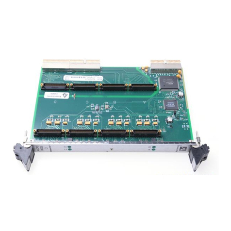
Acromag VPX4821A User manual

Artisan Technology Group is your source for quality
new and certied-used/pre-owned equipment
• FAST SHIPPING AND
DELIVERY
• TENS OF THOUSANDS OF
IN-STOCK ITEMS
• EQUIPMENT DEMOS
• HUNDREDS OF
MANUFACTURERS
SUPPORTED
• LEASING/MONTHLY
RENTALS
• ITAR CERTIFIED
SECURE ASSET SOLUTIONS
SERVICE CENTER REPAIRS
Experienced engineers and technicians on staff
at our full-service, in-house repair center
WE BUY USED EQUIPMENT
Sell your excess, underutilized, and idle used equipment
We also offer credit for buy-backs and trade-ins
www.artisantg.com/WeBuyEquipment
REMOTE INSPECTION
Remotely inspect equipment before purchasing with
our interactive website at www.instraview.com
LOOKING FOR MORE INFORMATION?
Visit us on the web at www.artisantg.com for more
information on price quotations, drivers, technical
specications, manuals, and documentation
Contact us: (888) 88-SOURCE | sales@artisantg.com | www.artisantg.com
SM
View
Instra

Carrier Card Series
VPX4821A/VPX4821A-CC VPX XMC/PMC Carrier
USER’S MANUAL
ACROMAG INCORPORATED
30765 South Wixom Road
Wixom, MI 48393-2417 U.S.A.
Tel: (248) 295-0310
Email: solutions@acromag.com
Copyright 2017, Acromag, Inc., Printed in the USA.
Data and specifications are subject to change without notice.
8501117D

CARRIER CARD SERIES VPX4821A XMC/PMC CARRIER
-
2
-
Contents
1. GENERAL INFORMATION......................................................................................................................... 4
KEY VPX4821A FEATURES........................................................................................................................ 4
2. PREPARATION FOR USE ........................................................................................................................... 6
UNPACKING AND INSPECTION ................................................................................................................ 6
CARD CAGE CONSIDERATIONS ........................................................................................................... 6
Board Configuration ........................................................................................................................... 6
JUMPERS............................................................................................................................................. 7
PCIe Lane Configuration..................................................................................................................... 7
PCIe Upstream Port Select ................................................................................................................. 8
Fan-Out Enable................................................................................................................................... 8
PCIe NT Port Enable/Select ................................................................................................................ 8
+3.3_AUX Power................................................................................................................................. 9
JTAG Reference Power ....................................................................................................................... 9
Clock Settings ..................................................................................................................................... 9
Reset................................................................................................................................................. 10
I2C PROGRAMMING............................................................................................................................... 10
NVROM............................................................................................................................................. 11
LED’s ...................................................................................................................................................... 11
BACKPLANE KEY..................................................................................................................................... 11
CONNECTORS ........................................................................................................................................ 11
VPX Connectors ................................................................................................................................ 14
PMC Connectors............................................................................................................................... 16
XMC Connectors............................................................................................................................... 20
FIELD GROUNDING CONSIDERATIONS .................................................................................................. 23
3. VPX CONNECTIVITY................................................................................................................................ 24
VITA 65 PROFILES .................................................................................................................................. 24
REAR I/O ................................................................................................................................................ 24
4. SERVICE AND REPAIR............................................................................................................................. 26
SERVICE AND REPAIR ASSISTANCE ........................................................................................................ 26
PRELIMINARY SERVICE PROCEDURE ................................................................................................ 26
WHERE TO GET HELP ............................................................................................................................. 26
5. SPECIFICATIONS..................................................................................................................................... 27
PHYSICAL................................................................................................................................................ 27
Physical Configuration...................................................................................................................... 27
Connectors ....................................................................................................................................... 27

CARRIER CARD SERIES VPX4821A XMC/PMC CARRIER
-
3
-
Jumpers ............................................................................................................................................ 27
POWER................................................................................................................................................... 27
XMC/PMC Power.............................................................................................................................. 28
Power Dissipation............................................................................................................................. 28
PCIe BUS COMPLIANCE.......................................................................................................................... 30
PCI BUS COMPLIANCE............................................................................................................................ 31
XMC/PMC Slot Selection ....................................................................................................................... 31
Rear I/O ................................................................................................................................................. 31
ENVIRONMENTAL .................................................................................................................................. 31
ENVIRONMENTAL .................................................................................................................................. 31
EMC Compliance .............................................................................................................................. 31
Certificate of Volatility........................................................................................................................... 32
6. REVISION HISTORY................................................................................................................................. 32
The information contained in this manual is subject to change without notice. Acromag, Inc. makes no warranty
of any kind with regard to this material, including, but not limited to, the implied warranties of merchantability
and fitness for a particular purpose. Further, Acromag, Inc. assumes no responsibility for any errors that may
appear in this manual and makes no commitment to update, or keep current, the information contained in this
manual. No part of this manual may be copied or reproduced in any form, without the prior written consent of
Acromag, Inc.
IMPORTANT SAFETY CONSIDERATIONS
It is very important for the user to consider the possible adverse effects of power, wiring, component, sensor,
or software failures in designing any type of control or monitoring system. This is especially important where
economic property loss or human life is involved. It is important that the user employ satisfactory overall
system design. It is agreed between the Buyer and Acromag, that this is the Buyer's responsibility.

CARRIER CARD SERIES VPX4821A XMC/PMC CARRIER
-
4
-
1. GENERAL INFORMATION
The VPX4821A card is a 6U VPX non-intelligent XMC/PMC carrier board
designed for PCIe bus connection to the VPX Data Plane. The board supports
up to a 8x PCIe connection that is selectable via jumpers. The carrier enables
the use of XMC and PMC mezzanine I/O modules. The carrier card acts as an
adapter to route PCIe bus signals between the PCIe bus of your backplane and
either P15 connector of an XMC module card or P11 and P12 of a PMC Card.
Access to rear I/O is provided through connections to the backplane. XMC and
PCM modules with front I/O can be accessed though the front mounting
bracket.
The VPX4821A series is a 6U VPX Non-Intelligent XMC/PMC carrier board
designed for 4x/8x PCIe bus connection. The carrier card uses a PLX
Technology® PCIe Switch Chip (PEX 8734) and IDT Technology®PCIe to PCI
Bridge Chip (TSI384) to interface between the VPX PCIe bus and one
XMC/PMC mezzanine I/O module card.
Model VPX4821A-XX-LF is an air-cooled product which can be used for front
and rear I/O XMC/PMC mezzanine modules.
Model VPX4821A-XX-CC-LF is an extended temperature conduction-cooled
product which supports all Acromag FPGA modules. It only supports Rear I/O.
Model
Description
Temp Range
VPX4821A-42-LF
Air-cooled 6U VPX XMC/PMC Carrier
for Data Plane with VITA 42
0 to +70C
VPX4821A-42-CC-LF
Conduction-cooled 6U VPX XMC/PMC
Carrier for Data Plane with VITA 42
-40 to +85C1
VPX4821A-61-LF
Air-cooled 6U VPX XMC/PMC Carrier
for Data Plane with VITA 61
0 to +70C
VPX4821A-61-CC-LF
Conduction-cooled 6U VPX XMC/PMC
Carrier for Data Plane with VITA 61
-40 to +85C1
1. See Power Specifications for further information including power rating.
KEY VPX4821A FEATURES
PCI Express Interface: Up to Sixteen PCI Express Gen 1 or Gen 2 lanes are
connected to the VPX P1 connecter. This is the Data Plane. Lane
configuration is jumper selectable.
PCI Express Configuration: Jumper selectable for two x8 ports, four x4 ports,
or one x8 port and two x4 ports.
PCI and PC-X Compliant: Each slot supports up to 133MHz 64 bit PCI-X.
Upstream and NT Port Configuration: Selectable via jumper.
I/O: Support both Front and Rear I/O. CC model is Rear I/O only.

CARRIER CARD SERIES VPX4821A XMC/PMC CARRIER
-
5
-
Single Power Supply: The carrier only requires VPX to provide +12V to PS1.
The carrier will generate and supply the PMC/XMC modules with +5V and
+3.3V. The XMC VPWR pins are connected to +12V. This board can also run
off only the VPX PS3 +5V supply. Please contact the factory for details. All
AUX supplies are optional and are only required if used by the XMC/PMC
modules.
JTAG Programming Header: The VPX4821A carrier includes a programming
connector that mates with a Xilinx programmer for programming Acromag
FPGA products. Acromag XMC FPGA boards can be configured to route the
JTAG programming signals through the XMC P15/P25 connectors.
Figure 1: Block Diagram

CARRIER CARD SERIES VPX4821A XMC/PMC CARRIER
-
6
-
2. PREPARATION FOR USE
UNPACKING AND INSPECTION
Upon receipt of this product, inspect the shipping carton for evidence of
mishandling during transit. If the shipping carton is badly damaged or water
stained, request that the carrier's agent be present when the carton is
opened. If the carrier's agent is absent when the carton is opened and the
contents of the carton are damaged, keep the carton and packing material for
the agent's inspection.
For repairs to a product damaged in shipment, refer to the Acromag Service
Policy to obtain return instructions. It is suggested that salvageable shipping
cartons and packing material be saved for future use in the event the product
must be shipped.
This board is physically protected with packing material and electrically
protected with an anti static bag during shipment. It is recommended that the
board be visually inspected for evidence of mishandling prior to applying
power.
The board utilizes static sensitive components and should only be handled at
a static-safe workstation.
CARD CAGE CONSIDERATIONS
Refer to the specifications for loading and power requirements. Be sure that
the system power supplies are able to accommodate the power requirements
of the carrier board, plus the installed PMC/XMC modules, within the voltage
tolerances specified.
Adequate air circulation must be provided to prevent a temperature rise
above the maximum operating temperature and to prolong the life of the
electronics. If the installation is in an industrial environment and the board is
exposed to environmental air, careful consideration should be given to air-
filtering.
Board Configuration
Power should be removed from the board when changing jumper
configurations or when installing an XMC or PMC module, cables and field
wiring.

CARRIER CARD SERIES VPX4821A XMC/PMC CARRIER
-
7
-
Figure 2: Jumper Diagram
JUMPERS
There are six jumper blocks located on the board. The jumper blocks are
labeled J1, J2, J3, J4, J5, and J6. Within each jumper block there are multiple
jumper settings. A jumper can be used to shout post horizontally and
vertically. The jumper position is OPEN if no jumper is present. The jumper
position is SET if a jumper is present across the two pins. The description for
each jumper is described in the tables that follow. Bold Selections are the
factory default setting.
For rugged designs all jumpers can be replaced with 0 Ohm resistors. Please
contact the factory for details.
PCIe Lane Configuration
The VPX P1 PCIe lane configuration is selectable via the J1 jumper. Please
note that these strapping settings can be overwritten via a I2C write to the
PEX8734.
Table 2-1 PCIe Lane Jumper Configuration
PCIe Lane Configuration
J1 Jumper Configuration
5-6
5-7
6-8
1-2
1-3
2-4
8x-8x
O
S
O
S
O
O
4x-4x-4x-4x
O
O
S
O
O
S
8x-4x-4x
O
O
S
O
S
O
Default setting is 4x-4x-4x-4x with vertical jumbers J1 2-4 and 6-8 set.
The PCIe lane configuration determined the PCIe switch port naming
convention. Use Table 2-2 as a reference when selecting the upstream and
downstream port.

CARRIER CARD SERIES VPX4821A XMC/PMC CARRIER
-
8
-
Table 2-2 PCIe Port Naming Convention
PCIe Lane Configuration
Port Naming
L0-L3
L4-L7
L8-L11
L12-L15
8x-8x
Port 0
Port 1
4x-4x-4x-4x
Port 0
Port 1
Port 2
Port 3
8x-4x-4x
Port 0
Port 1
Port 2
PCIe Upstream Port Select
The PCIe Upstream port is selectable via the J3 jumper. Please note that these
strapping settings can be overwritten via a I2C write to the PEX8734.
Table 2-3 PCIe Upstream Port Jumper Selection
PCIe Lane Configuration
J3 Jumper Configuration
5-6
5-7
6-8
1-2
1-3
2-4
Port 0
O
S
O
O
S
O
Port 1
O
S
O
O
O
S
Port 2
O
S
O
S
O
O
Port 3
O
O
S
O
S
O
Default setting is Port 0 with vertical J3 jumbers 1-3 and 5-7 set.
Fan-Out Enable
Enable peer-to-peer (Downstream endpoint-to-Downstream endpoint) traffic
with jumper J5 9-10 set. If peer-to-peer (Downstream endpoint-to-
Downstream endpoint) traffic is not needed, this jumper can be left open.
Table 2-4 Fan-Out Enable Jumper Setting
Fan-Out Enable
J5 9-10
Enable
SET
Disable
OPEN
Default Fan-Out Enabled setting horizontal J5 jumber 9-10 set.
PCIe NT Port Enable/Select
To Enable the Non-Transparent (NT) Port of the PCIe switch, SET J5 and J2
jumpers as listed in table 2-5. Please note that these strapping settings can be
overwritten via a I2C write to the PEX8734. Non-Transparent selected
presents a processor as an endpoint rather than another memory system.

CARRIER CARD SERIES VPX4821A XMC/PMC CARRIER
-
9
-
Table 2-5 NT Enabled Jumper Settings
Select NT
Upstream Port
Jumper Configuration
J5
J2
1-2
1-3
2-4
5-6
5-7
6-8
1-2
1-3
2-4
Port 0
O
S
O
O
S
O
O
S
O
Port 1
O
S
O
O
S
O
O
O
S
Port 2
O
S
O
O
S
O
S
O
O
Port 3
O
S
O
O
O
S
O
S
O
NT Disable
S
O
O
S
O
O
S
O
O
Default setting is NT Disable with horizontal J5 jumber 1-2 set, 5-6 set, and
J2 jumper 1-2 set.
+3.3_AUX Power
The 3.3V_AUX power is required for proper operation of this board. For users
without this power supply available on the VPX backplane you can
alternatively use the onboard generated 3.3V.
Table 2-6 +3.3V_AUX Power Select Jumper Settings
Source of +3.3V-AUX
J6 7-8
J6 9-10
Onboard +3.3V
OPEN
SET
Backplane
SET
OPEN
WARNING! The J6 7-8 and J6 9-10 jumpers should both never be set. This
could cause damage to either the board or chassis power supply.
Default setting is +3.3V_AUX from Backplane with horizontal J6 7-8 jumber
set.
JTAG Reference Power
The pull-up voltage on the JTAG pins to XMC P15 and P25 can be selected as
either +2.5V or +3.3V. Refer to the XMC User’s Manual for proper voltage
selection. The jumper J3 9-10 is for slot A and the jumper J1 9-10 is for slot B.
Table 2-7 JTAG Power Select Jumper Settings
JTAG Ref Voltage
Slot
LOC
Setting
Slot A
J3 9-10
OPEN +3.3V SET +2.5V
Slot B
J1 9-10
OPEN +3.3V SET +2.5V
Default setting is +3.3V JTAG Ref with J3 9-10 jumber OPEN and J1 9-10
jumper OPEN.
Clock Settings
There are several clock options available for the user. These options are set on
J4 1-2, J4 3-4, and J4 5-6 jumpers. The default selection is to use the on-board
crystal to generate the 100MHz PCIe clock. This frequency is propagated to all
parts and XMC/PMC modules. Users also have the option to use a clock from
the VPX backplane. Note that this must be a 100MHz clock for proper

CARRIER CARD SERIES VPX4821A XMC/PMC CARRIER
-
10
-
operation. Refer to the table below for jumper settings. Spread spectrum
clocking is enabled when J4 3-4 is Set. Spread spectrum clocking should
always be disabled.
Table 2-8 Clock Jumper Settings
Global Clock Source
J4 1-2
J4 3-4
J4 5-6
On Board Crystal
OPEN
OPEN
OPEN
VPX SYSCLK
SET
OPEN
OPEN
Disable all CLK’s
OPEN
OPEN
SET
Default setting is On Board Crystal with J4 1-2, J4 3-4, and J4 5-6 jumpers
OPEN.
Reset
The reset delay circuit is enabled/disabled via configuration jumper J6.
This system reset is propagated to all parts XMC/PMC modules and
backplane.
Configuration jumper J2 is used to configure the on-board system reset delay
circuit. When enabled, the VPX SYSRESET signal will be held down on
power-up for a configurable amount of time. This can be used to allow extra
time for a particularly large FPGA program to load before reset is de-asserted
and the PCIe bus is enumerated, for instance.
Refer to the table below for jumper settings.
Table 2-9 Reset Output Generator Jumper Settings
Reset Output Generator
J6 1-2
J6 3-4
System Reset
OPEN
SET
Delay Circuit Reset
SET
OPEN
RESET OUTPUT TIME
JUMPER POSITION
J2 5-6
J2 7-8
J2 9-10
20ms
OPEN
OPEN
OPEN
189ms
OPEN
OPEN
SET
300ms
SET
OPEN
OPEN
572ms
OPEN
SET
OPEN
761ms
OPEN
SET
SET
I2C PROGRAMMING
The PEX8734 PCI switch can alternately be programmed via a simple I2C bus.
The I2C is accessed via the System Bus pins on the VPX backplane.
Furthermore the I2C bus is connected to both XMC modules. For further
information on programming using the I2C bus contact the factory.

CARRIER CARD SERIES VPX4821A XMC/PMC CARRIER
-
11
-
NVROM
The NVROM signal from the VPX Backplane is routed to the PCIe Switch
EEPROM as well as both XMC modules.
LED’s
The VPX4821A has several status LEDS. These LED’s are primarily used for
initial power-up status. The LEDs are located on the front of the card near the
J1 to J6 jumpers. The table below describes the functionality.
Table 2-10 LED
LED
Color
Description
DS1
Green
All power supplies are good.
DS2
Red
PMC A Only –PCIe Lane 1 has connected.
DS3
Red
PMC A Only –PCIe Lane 2 has connected.
DS4
Red
PMC A Only –PCIe Lane 3 has connected.
DS5
Red
PMC A Only –PCIe Lane 4 has connected.
DS6
Red
PMC B Only –PCIe Lane 1 has connected.
DS7
Red
PMC B Only –PCIe Lane 2 has connected.
DS8
Red
PMC B Only –PCIe Lane 3 has connected.
DS9
Red
PMC B Only –PCIe Lane 4 has connected.
DS10
Green
VPX PCIe Port 0 has successfully connected
DS11
Green
VPX PCIe Port 1 has successfully connected
DS12
Green
VPX PCIe Port 2 has successfully connected
DS13
Green
VPX PCIe Port 3 has successfully connected
DS14
Green
A Connection has been made to XMC/PMC Slot A.
DS15
Green
A Connection has been made to XMC/PMC Slot B.
DS16
Red
Fatal Error (non-recoverable)
DS17
Green
PCI INTA
BACKPLANE KEY
The VPX4821A is not keyed and will plug into any VPX backplane. Prior to
powerup, verify that VS1 is +12V. Any other voltage on VS1 may damage the
board.
CONNECTORS
Refer to Figure 3 for connector locations. Connectors on the VPX4821A
carrier consist of six VPX Backplane connectors, then 2 XMC connectors, and
four PMC connectors for each slot. These interface connectors are discussed
in the following sections.

CARRIER CARD SERIES VPX4821A XMC/PMC CARRIER
-
12
-
J11/J12/J13/J21/J22/J23................PMC PCI signals
J14/J25 ...........................................PMC user signals (Rear I/O)
J15/J25 ...........................................XMC PCIe signals
J16/J26 ..........................................XMC user signals (Rear I/O)
P0 ...................................................VPX Power and system signals.
P1…………………………………………………VPX Data Plane. This connects to all PCIe lanes.
P2 ...................................................VPX Expansion plane. This connector is not populated.
P3/P4..............................................PMC/XMC Slot A Rear I/O.
P5/P6..............................................PMC/XMC Slot B Rear I/O.

CARRIER CARD SERIES VPX4821A XMC/PMC CARRIER
-
13
-
Figure 3: Connector Locations

CARRIER CARD SERIES VPX4821A XMC/PMC CARRIER
-
14
-
VPX Connectors
Table 2-11 P0 –VPX Utility Signals
Pin
A
B
C
D
E
F
G
1
VS2
VS2
VS2
NC
+12V
+12V
+12V
2
VS2
VS2
VS2
NC
+12V
+12V
+12V
3
+5V
+5V
+5V
NC
+5V
+5V
+5V
4
NVMRO
P0_SYSRESET
GND
-12V_AUX
GND
SM3
SM2
5
I2C_DAT
I2C_CLK
GND
+3.3V_AUX
GND
GA4
GAP
6
GA0
GA1
GND
+12V_AUX
GND
GA2
GA3
7
JTAG_TRST
JTAG_TMS
GND
JTAG_TDI
JTAG_TDO
GND
JTAG_TCK
8
GND
REF_BUS_P
REF_BUS_N
GND
P0_REFCLK_P
P0_REFCLK_N
GND
All blue colored cells are Not Used in this design.
Table 2-12 P1 –VPX Data Plane
Pin
A
B
C
D
E
F
G
1
PCIE_L0_RXP
PCIE_L0_RXN
Gnd
PCIE_L0_TXP
PCIE_L0_TXN
Gnd
2
Gnd
PCIE_L1_RXP
PCIE_L1_RXN
Gnd
PCIE_L1_TXP
PCIE_L1_TXN
Gnd
3
PCIE_L2_RXP
PCIE_L2_RXN
Gnd
PCIE_L2_TXP
PCIE_L2_TXN
Gnd
4
Gnd
PCIE_L3_RXP
PCIE_L3_RXN
Gnd
PCIE_L3_TXP
PCIE_L3_TXN
Gnd
5
PCIE_L4_RXP
PCIE_L4_RXN
Gnd
PCIE_L4_TXP
PCIE_L4_TXN
Gnd
6
Gnd
PCIE_L5_RXP
PCIE_L5_RXN
Gnd
PCIE_L5_TXP
PCIE_L5_TXN
Gnd
7
PCIE_L6_RXP
PCIE_L6_RXN
Gnd
PCIE_L6_TXP
PCIE_L6_TXN
Gnd
8
Gnd
PCIE_L7_RXP
PCIE_L7_RXN
Gnd
PCIE_L7_TXP
PCIE_L7_TXN
Gnd
9
PCIE_L8_RXP
PCIE_L8_RXN
Gnd
PCIE_L8_TXP
PCIE_L8_TXN
Gnd
10
Gnd
PCIE_L9_RXP
PCIE_L9_RXN
Gnd
PCIE_L9_TXP
PCIE_L9_TXN
Gnd
11
PCIE_L10_RXP
PCIE_L10_RXN
Gnd
PCIE_L10_TXP
PCIE_L10_TXN
Gnd
12
Gnd
PCIE_L11_RXP
PCIE_L11_RXN
Gnd
PCIE_L11_TXP
PCIE_L11_TXN
Gnd
13
PCIE_L12_RXP
PCIE_L12_RXN
Gnd
PCIE_L12_TXP
PCIE_L12_TXN
Gnd
14
Gnd
PCIE_L13_RXP
PCIE_L13_RXN
Gnd
PCIE_L13_TXP
PCIE_L13_TXN
Gnd
15
PCIE_L14_RXP
PCIE_L14_RXN
Gnd
PCIE_L14_TXP
PCIE_L14_TXN
Gnd
16
Gnd
PCIE_L15_RXP
PCIE_L15_RXN
Gnd
PCIE_L15_TXP
PCIE_L15_TXN
Gnd
All blue colored cells are Not Used in this design.

CARRIER CARD SERIES VPX4821A XMC/PMC CARRIER
-
15
-
Table 2-13 P3 –PMC SLOT A Rear I/O
Pin
A
B
C
D
E
F
G
1
PMC1_RIO1_N
PMC1_RIO1_P
Gnd
PMC1_RIO0_N
PMC1_RIO0_P
Gnd
2
Gnd
PMC1_RIO3_N
PMC1_RIO3_P
Gnd
PMC1_RIO2_N
PMC1_RIO2_P
Gnd
3
PMC1_RIO5_N
PMC1_RIO5_P
Gnd
PMC1_RIO4_N
PMC1_RIO4_P
Gnd
4
Gnd
PMC1_RIO7_N
PMC1_RIO7_P
Gnd
PMC1_RIO6_N
PMC1_RIO6_P
Gnd
5
PMC1_RIO9_N
PMC1_RIO9_P
Gnd
PMC1_RIO8_N
PMC1_RIO8_P
Gnd
6
Gnd
PMC1_RIO11_N
PMC1_RIO11_P
Gnd
PMC1_RIO10_N
PMC1_RIO10_P
Gnd
7
PMC1_RIO13_N
PMC1_RIO13_P
Gnd
PMC1_RIO12_N
PMC1_RIO12_P
Gnd
8
Gnd
PMC1_RIO15_N
PMC1_RIO15_P
Gnd
PMC1_RIO14_N
PMC1_RIO14_P
Gnd
9
PMC1_RIO17_N
PMC1_RIO17_P
Gnd
PMC1_RIO16_N
PMC1_RIO16_P
Gnd
10
Gnd
PMC1_RIO19_N
PMC1_RIO19_P
Gnd
PMC1_RIO18_N
PMC1_RIO18_P
Gnd
11
PMC1_RIO21_N
PMC1_RIO21_P
Gnd
PMC1_RIO20_N
PMC1_RIO20_P
Gnd
12
Gnd
PMC1_RIO23_N
PMC1_RIO23_P
Gnd
PMC1_RIO22_N
PMC1_RIO22_P
Gnd
13
PMC1_RIO25_N
PMC1_RIO25_P
Gnd
PMC1_RIO24_N
PMC1_RIO24_P
Gnd
14
Gnd
PMC1_RIO27_N
PMC1_RIO27_P
Gnd
PMC1_RIO26_N
PMC1_RIO26_P
Gnd
15
PMC1_RIO29_N
PMC1_RIO29_P
Gnd
PMC1_RIO28_N
PMC1_RIO28_P
Gnd
16
Gnd
PMC1_RIO31_N
PMC1_RIO31_P
Gnd
PMC1_RIO30_N
PMC1_RIO30_P
Gnd
All blue colored cells are Not Used in this design.
Table 2-14 P4 –XMC SLOT A Rear I/O
Pin
A
B
C
D
E
F
G
1
XMC1_DP05_N
XMC1_DP05_P
Gnd
XMC1_DP04_N
XMC1_DP04_P
Gnd
2
Gnd
XMC1_DP07_N
XMC1_DP07_P
Gnd
XMC1_DP06_N
XMC1_DP06_P
Gnd
3
XMC1_DP09_N
XMC1_DP09_P
Gnd
XMC1_DP08_N
XMC1_DP08_P
Gnd
4
Gnd
XMC1_DP15_N
XMC1_DP15_P
Gnd
XMC1_DP14_N
XMC1_DP14_P
Gnd
5
XMC1_DP17_N
XMC1_DP17_P
Gnd
XMC1_DP16_N
XMC1_DP16_P
Gnd
6
Gnd
XMC1_DP19_N
XMC1_DP19_P
Gnd
XMC1_IO_B19
XMC1_IO_A19
Gnd
7
XMC1_DP01_N
XMC1_DP01_P
Gnd
XMC1_DP00_N
XMC1_DP00_P
Gnd
8
Gnd
XMC1_DP03_N
XMC1_DP03_P
Gnd
XMC1_DP02_N
XMC1_DP02_P
Gnd
9
XMC1_DP11_N
XMC1_DP11_P
Gnd
XMC1_DP10_N
XMC1_DP10_P
Gnd
10
Gnd
XMC1_DP13_N
XMC1_DP13_P
Gnd
XMC1_DP12_N
XMC1_DP12_P
Gnd
11
Gnd
Gnd
12
Gnd
Gnd
Gnd
13
Gnd
Gnd
14
Gnd
Gnd
Gnd
15
Gnd
Gnd
16
Gnd
Gnd
Gnd
All blue colored cells are Not Used in this design.

CARRIER CARD SERIES VPX4821A XMC/PMC CARRIER
-
16
-
Table 2-15 P5 –PMC SLOT B Rear I/O
Pin
A
B
C
D
E
F
G
1
PMC2_RIO1_N
PMC2_RIO1_P
Gnd
PMC2_RIO0_N
PMC2_RIO0_P
Gnd
2
Gnd
PMC2_RIO3_N
PMC2_RIO3_P
Gnd
PMC2_RIO2_N
PMC2_RIO2_P
Gnd
3
PMC2_RIO5_N
PMC2_RIO5_P
Gnd
PMC2_RIO4_N
PMC2_RIO4_P
Gnd
4
Gnd
PMC2_RIO7_N
PMC2_RIO7_P
Gnd
PMC2_RIO6_N
PMC2_RIO6_P
Gnd
5
PMC2_RIO9_N
PMC2_RIO9_P
Gnd
PMC2_RIO8_N
PMC2_RIO8_P
Gnd
6
Gnd
PMC2_RIO11_N
PMC2_RIO11_P
Gnd
PMC2_RIO10_N
PMC2_RIO10_P
Gnd
7
PMC2_RIO13_N
PMC2_RIO13_P
Gnd
PMC2_RIO12_N
PMC2_RIO12_P
Gnd
8
Gnd
PMC2_RIO15_N
PMC2_RIO15_P
Gnd
PMC2_RIO14_N
PMC2_RIO14_P
Gnd
9
PMC2_RIO17_N
PMC2_RIO17_P
Gnd
PMC2_RIO16_N
PMC2_RIO16_P
Gnd
10
Gnd
PMC2_RIO19_N
PMC2_RIO19_P
Gnd
PMC2_RIO18_N
PMC2_RIO18_P
Gnd
11
PMC2_RIO21_N
PMC2_RIO21_P
Gnd
PMC2_RIO20_N
PMC2_RIO20_P
Gnd
12
Gnd
PMC2_RIO23_N
PMC2_RIO23_P
Gnd
PMC2_RIO22_N
PMC2_RIO22_P
Gnd
13
PMC2_RIO25_N
PMC2_RIO25_P
Gnd
PMC2_RIO24_N
PMC2_RIO24_P
Gnd
14
Gnd
PMC2_RIO27_N
PMC2_RIO27_P
Gnd
PMC2_RIO26_N
PMC2_RIO26_P
Gnd
15
PMC2_RIO29_N
PMC2_RIO29_P
Gnd
PMC2_RIO28_N
PMC2_RIO28_P
Gnd
16
Gnd
PMC2_RIO31_N
PMC2_RIO31_P
Gnd
PMC2_RIO30_N
PMC2_RIO30_P
Gnd
All blue colored cells are Not Used in this design.
Table 2-16 P6 –XMC SLOT B Rear I/O
Pin
A
B
C
D
E
F
G
1
XMC2_DP05_N
XMC2_DP05_P
Gnd
XMC2_DP04_N
XMC2_DP04_P
Gnd
2
Gnd
XMC2_DP07_N
XMC2_DP07_P
Gnd
XMC2_DP06_N
XMC2_DP06_P
Gnd
3
XMC2_DP09_N
XMC2_DP09_P
Gnd
XMC2_DP08_N
XMC2_DP08_P
Gnd
4
Gnd
XMC2_DP15_N
XMC2_DP15_P
Gnd
XMC2_DP14_N
XMC2_DP14_P
Gnd
5
XMC2_DP17_N
XMC2_DP17_P
Gnd
XMC2_DP16_N
XMC2_DP16_P
Gnd
6
Gnd
XMC2_DP19_N
XMC2_DP19_P
Gnd
XMC2_IO_B19
XMC2_IO_A19
Gnd
7
XMC2_DP01_N
XMC2_DP01_P
Gnd
XMC2_DP00_N
XMC2_DP00_P
Gnd
8
Gnd
XMC2_DP03_N
XMC2_DP03_P
Gnd
XMC2_DP02_N
XMC2_DP02_P
Gnd
9
XMC2_DP11_N
XMC2_DP11_P
Gnd
XMC2_DP10_N
XMC2_DP10_P
Gnd
10
Gnd
XMC2_DP13_N
XMC2_DP13_P
Gnd
XMC2_DP12_N
XMC2_DP12_P
Gnd
11
Gnd
Gnd
12
Gnd
Gnd
Gnd
13
Gnd
Gnd
14
Gnd
Gnd
Gnd
15
Gnd
Gnd
16
Gnd
Gnd
Gnd
All blue colored cells are Not Used in this design.
PMC Connectors
Table 2-17 Jx1 PMC PCI Signals
Pin Description
Number
Pin Description
Number
TCK
1
-12V
2

CARRIER CARD SERIES VPX4821A XMC/PMC CARRIER
-
17
-
Pin Description
Number
Pin Description
Number
GND
3
INTA#
4
INTB#
5
INTC#
6
BUSMODE1#
7
+5V
8
INTD#
9
NC1
10
GND
11
+3.3VAUX
12
CLK
13
GND
14
GND
15
GNT#
16
REQ#
17
+5V
18
+3.3V
19
AD31
20
AD28
21
AD27
22
AD25
23
GND
24
GND
25
C/BE3#
26
AD22
27
AD21
28
AD19
29
+5V
30
+3.3V
31
AD17
32
FRAME#
33
GND
34
GND
35
IRDY#
36
DEVSEL#
37
+5V
38
PCIXCAP
39
LOCK#
40
NC1
41
NC1
42
PAR
43
GND
44
+3.3V
45
AD15
46
AD12
47
AD11
48
AD9
49
+5V
50
GND
51
C/BE0#
52
AD6
53
AD5
54
AD4
55
GND
56
+3.3V
57
AD3
58
AD2
59
AD1
60
AD0
61
+5V
62
GND
63
REQ64#
64
1. NC- Not used.
Table 2-18 Jx2 PMC PCI Signals
Pin Description
Number
Pin Description
Number
+12V
1
TRST#
2
TMS
3
TDO
4
TDI
5
GND
6
GND
7
NC1
8
NC1
9
NC1
10
BUSMODE2#
11
+3.3V
12
RST#
13
BUSMODE3#
14
+3.3V
15
BUSMODE4#
16
PME#
17
GND
18

CARRIER CARD SERIES VPX4821A XMC/PMC CARRIER
-
18
-
Pin Description
Number
Pin Description
Number
AD30
19
AD29
20
GND
21
AD26
22
AD24
23
+3.3V
24
IDSEL
25
AD23
26
+3.3V
27
AD20
28
AD18
29
GND
30
AD16
31
C/BE2#
32
GND
33
NC1
34
TRDY#
35
+3.3V
36
GND
37
STOP#
38
PERR#
39
GND
40
+3.3V
41
SERR#
42
C/BE1#
43
GND
44
AD14
45
AD13
46
M66EN
47
AD10
48
AD8
49
+3.3V
50
AD7
51
NC1
52
+3.3V
53
NC1
54
NC1
55
GND
56
NC1
57
NC1
58
GND
59
NC1
60
ACK64#
61
+3.3V
62
GND
63
NC1
64
1. NC- Not used.
Table 2-19 Jx3 PMC PCI Signals
Pin Description
Number
Pin Description
Number
NC1
1
GND
2
GND
3
C/BE7#
4
C/BE6#
5
C/BE5#
6
C/BE4#
7
GND
8
+3.3V
9
PAR64
10
AD63
11
AD62
12
AD61
13
GND
14
GND
15
AD60
16
AD59
17
AD58
18
AD57
19
GND
20
+3.3V
21
AD56
22
AD55
23
AD54
24
AD53
25
GND
26
GND
27
AD52
28
AD51
29
AD50
30
AD49
31
GND
32

CARRIER CARD SERIES VPX4821A XMC/PMC CARRIER
-
19
-
Pin Description
Number
Pin Description
Number
GND
33
AD48
34
AD47
35
AD46
36
AD45
37
GND
38
+3.3V
39
AD44
40
AD43
41
AD42
42
AD41
43
GND
44
GND
45
AD40
46
AD39
47
AD38
48
AD37
49
GND
50
GND
51
AD36
52
AD35
53
AD34
54
AD33
55
GND
56
+3.3V
57
AD32
58
NC1
59
NC1
60
NC1
61
GND
62
GND
63
NC1
64
1. NC- Not used.
Table 2-20 Jx4 PMC PCI Rear I/O Signals
Pin Description
Number
Pin Description
Number
RIO0_P
1
RIO1_P
2
RIO0_N
3
RIO1_N
4
RIO2_P
5
RIO3_P
6
RIO2_N
7
RIO3_N
8
RIO4_P
9
RIO5_P
10
RIO4_N
11
RIO5_N
12
RIO6_P
13
RIO7_P
14
RIO6_N
15
RIO7_N
16
RIO8_P
17
RIO9_P
18
RIO8_N
19
RIO9_N
20
RIO10_P
21
RIO11_P
22
RIO10_N
23
RIO11_N
24
RIO12_P
25
RIO13_P
26
RIO12_N
27
RIO13_N
28
RIO14_P
29
RIO15_P
30
RIO14_N
31
RIO15_N
32
RIO16_P
33
RIO17_P
34
RIO16_N
35
RIO17_N
36
RIO18_P
37
RIO19_P
38
RIO18_N
39
RIO19_N
40
RIO20_P
41
RIO21_P
42
RIO20_N
43
RIO21_N
44
RIO22_P
45
RIO23_P
46
This manual suits for next models
1
Table of contents
Other Acromag PCI Card manuals
Popular PCI Card manuals by other brands
NETGEAR
NETGEAR WG311 installation guide

Milestone
Milestone PRO MP-HU3VC-H2 user manual
D-Link
D-Link AirPlus XTREME G DWL-G520 manual

THOMSON
THOMSON Grass Valley Pegasus Reviewer's guide
Neousys Technology
Neousys Technology PCIe-USB380 user manual

Comtrol
Comtrol RocketPort PCI Series Hardware installation guide
