AeroComm AC4490 User manual


DOCUMENT INFORMATION
Copyright Copyright © 2005 AEROCOMM, Inc. All rights reserved.
The information contained in this manual and the accompanying
software programs are copyrighted and all rights are reserved by
AEROCOMM, Inc. AEROCOMM, Inc. reserves the right to make
periodic modifications of this product without obligation to notify
any person or entity of such revision. Copying, duplicating, selling, or otherwise
distributing any part of this product or accompanying documentation/software
without the prior consent of an authorized representative of AEROCOMM, Inc. is
strictly prohibited.
All brands and product names in this publication are registered
Information
trademarks or trademarks of their respective holders.
AEROCOMM’s products are intended for use in normal commercial and industrial applications.
Applications requiring unusual environmental requirements such as military, medical life-support or
life-sustaining equipment are specifically not recommended without additional testing for such
application.
Information furnished by AEROCOMM in this specification is believed to be accurate. Devices sold
by AEROCOMM are covered by the warranty and patent indemnification provisions appearing in its
Terms of Sale only. AEROCOMM makes no warranty, express, statutory, and implied or by
description, regarding the information set forth herein. AEROCOMM reserves the right to change
specifications at any time and without notice.
This material is preliminary
If, after inspection, AeroComm determines that there is a defect, AeroComm will repair or
replace the OEM transceiver at their discretion. If the product is replaced, it may be a new or
refurbished product.
In no event shall AeroComm be responsible or liable for any damages arising: From the use
of product; From the loss of use, revenue or profit of the product; or As a result of any event,
circumstance, action, or abuse beyond the control of AeroComm, whether such damages be
direct, indirect, consequential, special or otherwise and whether such damages are incurred
by the person to whom this warranty extends or third party.
This warranty does not cover and AeroComm will not be liable for, any damage or failure
caused by misuse, abuse, acts of God, accidents, electrical irregularity, or other causes
beyond AeroComm’s control, or claim by other than the original purchaser.
For a period of one (1) year from the date of purchase by the OEM customer, AeroComm
warrants the OEM transceiver against defects in materials and workmanship. AeroComm will
not honor this warranty (and this warranty will be automatically void) if there has been any (1)
tampering, signs of tampering; 2) repair or attempt to repair by anyone other than an
AeroComm authorized technician.
Limited Warranty, Disclaimer, Limitation of Liability
12/20/05 2

DOCUMENT INFORMATION
Revision Description
Version 1.0 3/15/2002 – Initial Release Version
Version 1.1 12/18/2002 – Preliminary Release
Version 1.2 12/20/2002 – Preliminary Release. Changed location of new interface pins for higher
compatibility with AC4424 product family.
Version 1.3 1/29/2003 – Updated interface baud rate formula/table. Updated current consumption
table. Corrected RSSI plot. Updated Interface Timeout information. Renamed product
family to AC4490. Multiple byte EEPROM read/write now allowed.
Version 1.4 2/18/2003 – Added Max Power byte. Removed Write Enable references. Fixed Power
Down/Up command response. Removed Peer-to-Peer bit. Added Auto Destination.
Added Unicast Only bit. Added 500mW product. Revised part numbers. Updated
Channel Number settings.
Version 1.5 Not released.
Version 1.6 11/07/2003 – Added One Beacon and modem modes. Included AC4486 product line.
Added 500mW specifications. Updated part numbers. Added AT Commands.
Eliminated Commercial designation: All transceivers are now industrial qualified.
Version 1.7 7/09/04 – Changed Range Refresh so that 0h is an invalid setting. Updated AC4490
500mW output power (conducted and EIRP). Added warranty information. Changed
AC4490-500 part number to AC4490-1000. Removed support of One Beacon Mode.
Added DES.
Version 1.8 1/03/04 – Changed minimum Interface Timeout @ 19,200 baud to 3. Added support for
One Beacon Mode. Changed voltage requirements for -200 module. Added on-the-fly
Read Temperature command. Added on-the-fly EEPROM read/write commands.
Removed AC4486 product information. Added Auto Channel.
Version 1.9 7/29/05 – Removed documentation for static commands. Added Australian Channels.
Added CC 26 command. Updated mechanical drawing (updated third mounting hole
location) for MMCX version. Included new RSSI table. Added 1x1 documentation.
Added Protocol Status, Received Acknowledge and Receive API modes.
Version 2.0 9/6/05 – Added Appendix I - Power Supply Application Note.
Version 2.1 10/6/05 – Added CC 27 command. Added Long Range Mode. Added EEPROM write
warning.
Version 2.2 11/8/05 – Removed CC 27 command. Removed Long Range mode. Corrected
RS-485 DE Control.
Version 2.3 12/20/05 – Removed Stream mode documentation. Added Enhanced API features.
Updated Australia channels.
12/20/05 3

TABLE OF CONTENTS
1. OVERVIEW............................................................................................................................7
2. AC4490 SPECIFICATIONS ..................................................................................................8
3. SPECIFICATIONS.................................................................................................................9
3.1 INTERFACE SIGNAL DEFINITIONS .........................................................................................................9
3.2 ELECTRICAL SPECIFICATIONS.............................................................................................................10
3.3 SYSTEM TIMING AND LATENCY..........................................................................................................11
3.3.1 Serial Interface Data Rate.........................................................................................................11
3.3.2 Latency ......................................................................................................................................11
3.3.3 Timing Diagrams.......................................................................................................................13
3.3.4 Maximum Overall System Throughput......................................................................................14
4. CONFIGURING THE AC4490.............................................................................................15
4.1 EEPROM PARAMETERS.....................................................................................................................15
4.2 CONFIGURATION FLOW OF THE AC4490 ............................................................................................18
4.3 COMMAND QUICK REFERENCE...........................................................................................................19
4.4 EEPROM CONFIGURATION COMMANDS ...........................................................................................21
4.4.1 EEPROM Byte Read..................................................................................................................21
4.4.2 EEPROM Byte Write .................................................................................................................21
4.4.3 EEPROM Exit Configuration Mode Command.........................................................................22
4.5 AC4490 AT COMMANDS ...................................................................................................................22
4.5.1 Enter AT Command Mode.........................................................................................................22
4.5.2 AT Enter Configuration Mode...................................................................................................23
4.5.3 Exit AT Command Mode............................................................................................................23
4.6 ON-THE-FLY CONTROL COMMANDS (CC COMMAND MODE) ............................................................23
4.6.1 Status Request............................................................................................................................24
4.6.2 Change Channel without Forced Acquisition Sync...................................................................24
4.6.3 Change Channel with Forced Acquisition Sync ........................................................................24
4.6.4 Server/Client Command.............................................................................................................24
4.6.5 Sync to Channel Command........................................................................................................25
4.6.6 Sleep Walk Power-Down Command..........................................................................................25
4.6.7 Sleep Walk Power-Down Wake-Up Command..........................................................................26
4.6.8 Broadcast Mode.........................................................................................................................26
4.6.9 Write Destination Address.........................................................................................................26
4.6.10 Read Destination Address..........................................................................................................26
4.6.11 Auto Channel / Auto Destination...............................................................................................27
4.6.12 Read Digital Inputs....................................................................................................................27
4.6.13 Read ADC..................................................................................................................................28
4.6.14 Report Last Valid RSSI..............................................................................................................28
4.6.15 Write Digital Outputs ................................................................................................................29
4.6.16 Write DAC.................................................................................................................................29
4.6.17 Set Max Power...........................................................................................................................30
4.6.18 Transmit Buffer Empty...............................................................................................................30
4.6.19 Disable Sync to Channel............................................................................................................31
4.6.20 Deep Sleep Mode.......................................................................................................................31
4.6.21 Read Temperature .....................................................................................................................31
4.6.22 EEPROM Byte Read..................................................................................................................31
4.6.23 EEPROM Byte Write .................................................................................................................32
4.6.24 Reset Command.........................................................................................................................32
5. THEORY OF OPERATION .................................................................................................33
12/20/05 4

5.1 HARDWARE INTERFACE......................................................................................................................33
5.1.1 GIn (Generic Inputs 0 and 1) (pins 4 and 14 respectively) and GOn (Generic Outputs 0 and 1)
(pins 1 and 9 respectively).........................................................................................................................33
5.1.2 TXD (Transmit Data) and RXD (Receive Data) (pins 2 and 3 respectively).............................33
5.1.3 Hop Frame (pin 6).....................................................................................................................33
5.1.4 CTS Handshaking (pin 7)..........................................................................................................34
5.1.5 RTS Handshaking (pin 8)...........................................................................................................34
5.1.6 9600 Baud (pin 12)....................................................................................................................34
5.1.7 RSSI (pin 13)..............................................................................................................................34
5.1.8 UP_Reset (pin 15) .....................................................................................................................35
5.1.9 Command/Data (pin 17)............................................................................................................35
5.1.10 AD In and DA Out (pins 18 and 19 respectively)......................................................................36
5.1.11 In Range (pin 20).......................................................................................................................36
5.2 SOFTWARE PARAMETERS ...................................................................................................................36
5.2.1 RF Architecture (Unicast/Broadcast)........................................................................................36
5.2.2 RF Mode....................................................................................................................................36
5.2.3 Sub Hop Adjust..........................................................................................................................37
5.2.4 Duplex Mode .............................................................................................................................37
5.2.5 Interface Timeout/RF Packet Size..............................................................................................37
5.2.6 Serial Interface Baud Rate.........................................................................................................38
5.2.7 Network Topology......................................................................................................................38
5.2.8 Auto Config................................................................................................................................40
5.2.9 One Beacon Mode .....................................................................................................................41
5.2.10 Max Power.................................................................................................................................42
5.2.11 Interface Options.......................................................................................................................44
5.2.12 Protocol Status and Received Acknowledgment........................................................................45
5.2.13 Receive API ...............................................................................................................................45
5.2.14 Enhanced Receive API...............................................................................................................45
5.2.15 Transmit API Packet..................................................................................................................46
5.2.16 API Send Data Complete...........................................................................................................46
6. DIMENSIONS......................................................................................................................47
7. ORDERING INFORMATION...............................................................................................52
7.1 PRODUCT PART NUMBER TREE ..........................................................................................................52
7.2 DEVELOPER KIT PART NUMBERS.......................................................................................................52
8. AGENCY COMPLIANCY INFORMATION..........................................................................53
8.1 AC4490-1X1......................................................................................................................................53
8.2 AGENCY IDENTIFICATION NUMBERS..................................................................................................53
8.3 APPROVED ANTENNA LIST.................................................................................................................54
FCC /INDUSTRY CANADA (IC) REQUIREMENTS FOR MODULAR APPROVAL..................................................55
8.3.1 OEM Equipment Labeling Requirements ..................................................................................55
8.3.2 Antenna Requirements...............................................................................................................55
8.3.3 Warnings Required in OEM Manuals .......................................................................................56
8.3.4 Channel Warning.......................................................................................................................56
9. APPENDIX I - POWER SUPPLY APPLICATION NOTE ...................................................57
9.1 OVERVIEW .........................................................................................................................................57
Figures
Figure 1 – RSSI Voltage vs. Received Signal Strength ................................................................ 35
Figure 2 - AC4490 (with MMCX Connector) Mechanical .............................................................. 47
Figure 3 - AC4490 (with Integral GigaAnt Antenna on Top) Mechanical...................................... 48
Figure 4 - AC4490 (with Integral GigaAnt Antenna on Bottom) Mechanical................................. 49
12/20/05 5

Figure 5 - AC4490-1x1 Mechanical............................................................................................... 50
Figure 6 - AC4490-1x1 PCB Considerations................................................................................. 51
Tables
Table 1 – Pin Definitions.................................................................................................................. 9
Table 2 - Input Voltage Characteristics (AC4490-1000 and AC4490-1x1) ................................... 10
Table 3 – Input Voltage Characteristics (All Others)..................................................................... 10
Table 4 – Output Voltage Characteristics (All).............................................................................. 11
Table 5 – Supported Serial Formats..............................................................................................11
Table 6 – Timing Parameters........................................................................................................ 14
Table 7 – Maximum Overall System Throughputs........................................................................ 14
Table 8 – EEPROM Parameters ................................................................................................... 15
Table 9 – Baud Rate/Interface Timeout ........................................................................................ 38
Table 10 – US and International RF Channel Number Settings ................................................... 40
Table 11 – Auto Config Parameters.............................................................................................. 41
Table 12 – One Beacon Mode Settings ........................................................................................ 41
Table 13 – Current versus Output Power for AC4490-1x1 Transmitter............................................. 42
Table 14 – Current versus Output Power for AC4490-200 Transmitter........................................ 42
Table 15 – Current versus Output Power for AC4490-1000 Transmitter...................................... 43
Table 16 – Transceiver Interface to DCE (Server Transceiver).................................................... 44
Table 17 – Transceiver Interface to DTE (Client Transceiver)...................................................... 44
Table 18 – Agency Identification Numbers.................................................................................... 53
Table 19 – AC4490 Approved Antenna List.................................................................................. 54
12/20/05 6

AC4490 Specifications
AC4490 Features
9Drop-in replacement for AC4424 2.4GHz product family
9Two generic input and output digital lines and integrated DAC/ADC functions
9Frequency Hopping Spread Spectrum for security and interference rejection
9Cost Effective for high volume applications
9Very low power consumption for battery powered implementations
9Small size for portable and enclosed applications
9Very Low latency and high throughput
9All modules are qualified for Industrial temperatures (-40°C to 80°C)
1. Overview
The AC4490 is a member of AeroComm’s ConnexRF OEM transceiver family. The AC4490 is
designed for integration into OEM systems operating under FCC part 15.247 regulations for the 900
MHz ISM band.
The AC4490 is a cost-effective, high performance, frequency hopping spread spectrum transceiver. It
provides an asynchronous TTL/RS-485 level serial interface for OEM Host communications.
Communications include both system and configuration data. The Host supplies system data for
transmission to other Host(s). Configuration data is stored in an on-board EEPROM. All frequency
hopping, synchronization, and RF system data transmission/reception is performed by the transceiver.
These transceivers can be used as a direct serial cable replacement – requiring no special Host
software for operation. They also feature a number of On-the-Fly Control Commands providing the
OEM with a very versatile interface for any network.
AC4490 transceivers operate in a Point-to-Point or Point-to-Multipoint, Client-Server or Peer-to-Peer
architecture. One transceiver is configured as a Server and there can be one or many Clients. To
establish synchronization between transceivers, the Server emits a beacon. Upon detecting a beacon,
a Client transceiver informs its Host and a RF link is established.
This document contains information about the hardware and software interface between an AeroComm
AC4490 transceiver and an OEM Host. Information includes the theory of operation, specifications,
interface definition, configuration information and mechanical drawings.
The OEM is responsible for ensuring the final product meets all appropriate regulatory agency
requirements listed herein before selling any product.
12/20/05 7

AC4490 Specifications
2. AC4490 Specifications
GENERAL
20 Pin Interface Connector Samtec TMM-110-01-L-D-SM, mates with Samtec SMM-110-02-S-D
RF Connector MMCX receptacle, mates with any manufacturer’s MMCX style plug
Antenna AC4490-1x1: Customer must provide
AC4490-200: MMCX Connector or integral antenna
AC4490-1000: MMCX Connector
Serial Interface Data Rate Baud rates from 1200 bps to 115,200 bps
Power Consumption (typical) Duty Cycle (TX=Transmit; RX=Receive)
10%TX 50%TX 100%TX 100%RX Pwr-DownDeep Sleep
AC4490-1x1: 33mA 54mA 80mA 28mA 15mA 3mA
AC4490-200: 38mA 68mA 106mA 30mA 19mA 6mA
AC4490-1000:130mA 650mA 1300mA 30mA 19mA 6mA
Channels 3 Channel Sets comprising 56 total channels
Security One byte System ID. 56 bit DES encryption key.
Interface Buffer Size Input/Output: 256 bytes each
TRANSCEIVER
Frequency Band 902 – 928 MHz
RF Data Rate 76.8kbps fixed
RF Technology Frequency Hopping Spread Spectrum
Output Power Conducted (no antenna) EIRP (3dBi gain antenna)
AC4490-1x1: 10mW typical 20mW typical
AC4490-200: 100mW typical 200mW typical
AC4490-1000: 743mW typical 1486mW typical
Supply Voltage AC4490-1x1: 3.3V, ±50mV ripple
AC4490-200: 3.3 – 5.5V, ±50mV ripple
AC4490-1000: Pin 10: 3.3 – 5.5V ±50mV ripple
Pin 11: 3.3 ±3%, ±100mV ripple
Sensitivity -99dBm typical @ 76.8kbps RF Data Rate
Range, Line of Site (based on
3dBi gain antenna) AC4490-1x1: 1 mile
AC4490-200: 4 miles
AC4490-1000: 20 miles
ENVIRONMENTAL
Temperature (Operating) -40°C to 80°C
Temperature (Storage) -50°C to +85°C
Humidity (non-condensing) 10% to 90% PHYSICAL
Dimensions Transceiver with MMCX Connector: 1.65” x 1.9” x 0.20”
Transceiver with Integral Antenna: 1.65” x 2.65” x 0.20”
AC4490-1x1: 1.00” x 1.00” x 0.162”
Weight Less than 0.75 ounce
12/20/05 8

AC4490 Specifications
3. Specifications
3.1 INTERFACE SIGNAL DEFINITIONS
The table below shows the connector pin numbers and associated functions. The I/O direction is with
respect to the transceiver. All outputs are 3.3VDC levels and inputs are 5VDC TTL (with the exception
of AC4490-1x1 and AC4490-1000 transceivers which have 3.3V inputs). All inputs are weakly pulled
High and may be left floating during normal operation (with the exceptions listed for the AC4490-1x1).
Table 1 – Pin Definitions
Module
Pin 1x1
Pin Type Signal Name Function
1 4 Output GO0 Generic Output pin
6 Output TXD Transmitted data out of the transceiver
2 N/A I/O RS485 A
(True)1Non-inverted RS-485 representation of serial data
7 Input RXD Data inputto the transceiver
3 N/A I/O RS485 B
(Invert)1 Inverse of RS-485 A
4 52Input GI0 Generic Input pin
5,16 3,13 GND GND Signal Ground
6 1 Output Hop Frame Pulses Low when the transceiver is hopping.
7 9 Output CTS Clear to Send – Active Low when the transceiver is ready to accept data for transmission.
8 102 Input RTS
Request to Send –When enabledin EEPROM, the OEM Host can take this High when it is notready to accept
data from the transceiver. Keeping RTS High for too long can cause data loss.
9 19 Output GO1 Generic Output pin
10,11 2,11 PWR VCC
AC4490-1x1: 3.3V, ±50mV ripple
AC4490-200: 3.3 – 5.5V, ±50mV ripple
AC4490-1000: Pin 10 (digital supply): 3.3 – 5.5V, ±50mV ripple, 50mA max
Pin 11 (Power Amplifier supply): 3.3V ±3%, ±100mV ripple, 1.3A max
12 23 Input 9600_BAUD
9600_BAUD– When pulled logic Low and then applying power or resetting, the transceiver’s serial interface is
forced to a 9600, 8, N, 1 rate. To exit, transceiver must be reset or power-cycled with 9600_Baud logic High.
13 12 Output RSSI
Received Signal Strength - An analog output giving an instantaneous indication of received signal strength. Only
valid while in Receive Mode.
14 212Input GI1 Generic Input pin
15 16 Input UP_RESET
RESET – Controlled by the AC4490 for power-on reset if left unconnected. After a Stable power-on reset, a logic
High pulse will reset the transceiver.
17 17 Input Command/Data
When logic Low, the transceiver interprets Host data as command data. When logic High, the transceiver interprets
Host data as transmit data.
18 153Input AD In 10 bit Analog Data Input
19 204Output DA Out 10 bit Analog Data Output
20 18 Output IN_RANGE
In Range – Active Low when a Client transceiver is in range of a Server on same Channel with the same SystemID. Always
Low on a Server (unless Sync-to-Channel is enabled).
N/A 14 RF RF PORT RFInterface.
N/A 22 Input RESET Active LowversionofUP_RESET. If RESET is used, UP_RESET should be left floating.
1When ordered with a RS-485 interface (not available on the AC4490-1x1).
2Must be tied to VCC or GND if not used. Should never be permitted to float.
3If used, requires a shunt 0.1μF capacitor at pin 15 followed by a series 1kΩresistor.
4If used, requires a series 1kΩresistor at pin 20 followed by a shunt 0.1μF capacitor.
12/20/05 9

AC4490 Specifications
N/A 8,24-28 N/C No Connect These pins have an internal connection and should be left floating.
3.2 ELECTRICAL SPECIFICATIONS
Table 2 - Input Voltage Characteristics (AC4490-1000 and AC4490-1x1)
-1000
Pin -1x1
Pin Type Name High
Min. High
Max. Low
Min. Low
Max. Unit
2,3 N/A I/O RS485A/B N/A 12 -7 N/A V
3 7 I RXD 2.24 3.3 0 0.96 V
4 5 I GI0 2.24 3.3 0 0.96 V
8 10 I RTS 2.24 3.3 0 0.96 V
12 23 I 9600_Baud 2.24 3.3 0 0.96 V
14 21 I GI1 2.24 3.3 0 0.96 V
15 16 I UP_RESET 0.8 3.3 0 0.6 V
17 17 I Command/Data 2.24 3.3 0 0.96 V
18 15 I AD In N/A 3.3 0 N/A V
N/A 22 I UP_RESET 2.24 3.3 0 0.96 V
Table 3 – Input Voltage Characteristics (All Others)
Pin Type Name High Min. High Max. Low Min. Low Max. Unit
2,3 I/O RS485A/B N/A 12 -7 N/A V
3 I RXD 2 5.5 0 0.8 V
4 I GI0 2 5.5 0 0.8 V
8 I RTS 2 5.5 0 0.8 V
12 I 9600_Baud 2 5.5 0 0.8 V
14 I GI1 2 5.5 0 0.8 V
15 I UP_RESET 0.8 5 0 0.6 V
17 I Command/Data 2 5.5 0 0.8 V
18 I AD In N/A 3.3 0 N/A V
12/20/05 10

AC4490 Specifications
Table 4 – Output Voltage Characteristics (All)
Module
Pin 1x1
Pin Type Name High Min. Low Max. Unit
1 4 O GO0 2.5 @ 8mA 0.4 @ 8mA V
2 6 O TXD 2.5 @ 2mA 0.4 @ 2mA V
2,3 N/A I/O RS485A/B 3.3 @ 1/8 Unit Load N/A V
6 1 O Hop Frame 2.5 @ 2mA 0.4 @ 2mA V
7 9 O CTS 2.5 @ 2mA 0.4 @ 2mA V
9 19 O GO1 2.5 @ 2mA 0.4 @ 2mA V
13 12 O RSSI See Figure 1 See Figure 1 V
19 20 O DA Out N/A N/A V5
20 18 O IN_RANGE 2.5 @ 2mA 0.4 @ 2mA V
3.3 SYSTEM TIMING AND LATENCY
Care should be taken when selecting transceiver architecture as it can have serious effects on data
rates, latency timings, and overall system throughput. The importance of these three characteristics
will vary from system to system and should be a strong consideration when designing the system.
3.3.1 Serial Interface Data Rate
The Serial Interface Data Rate is programmable by the Host. This is the rate the Host and transceiver
communicate over the serial bus. Possible values range from 1200 bps to 115,200 bps. Note:
Enabling Parity Mode cuts throughput in half and the Interface Buffer size in half. The following
asynchronous serial data formats are supported:
Table 5 – Supported Serial Formats
Data Bits Parity Stop Bits Transceiver Programming
Requirements
9 N 1 Parity Mode enabled
8 N 1 Parity Mode disabled
8 N 2 Parity Mode enabled
8 E,O,M,S 1 Parity Mode enabled
7 E,O,M,S 2 Parity Mode enabled
7 N 2 Parity mode disabled
7 E,O,M,S 1 Parity Mode disabled
3.3.2 Latency
Acknowledge Mode
The transceiver will use Interface Timeout in conjunction with Fixed Packet Length (whichever condition
occurs first) to determine a complete packet to be sent over the RF. If Full Duplex is enabled, the
5DA Out is an unbuffered, high impedance output and must be buffered by the OEM Host when
used.
12/20/05 11

AC4490 Specifications
transceiver must wait for its appropriate hop (even numbered hops for the Server and odd numbered
hops for the Client). Upon doing this, the transceiver will calculate the amount of time until the next hop
to ensure that it has time to send the packet. If there is enough time, it will send the packet: if not, it will
wait until its next appropriate hop. Transmit Retries and Broadcast Attempts are handled in this same
manner.
12/20/05 12

AC4490 Specifications
3.3.3 Timing Diagrams
Addressed Acknowledge Mode with Interface Timeout:
Local_RXD
Local_RF_TXD
Remote_RF_TXD
Remote_TXD
Hop_Frame
Packet Data
RF Packet
Received Data
RF Acknowledge
Hop Time
Hop Period
Interface Timeout
Wait for Hop
Addressed Acknowledge Mode with Fixed Packet Length:
Local_RXD
Local_RF_TXD
Remote_RF_TXD
Remote_TXD
Hop_Frame
Packet Data
RF Packet
Received Data
RF Acknowledge
Hop Time
Wait for Hop
Hop Period
Broadcast Acknowledge Mode with Interface Timeout:
Local_RXD
Local_RF_TXD
Remote_RF_TXD
Remote_TXD
Hop_Frame
Packet Data
RF Packet
Received Data
Hop Time
Hop Period
Interface Timeout
Wait for Hop
12/20/05 13

AC4490 Specifications
Broadcast Acknowledge Mode with Fixed Packet Length:
Local_RXD
Local_RF_TXD
Remote_RF_TXD
Remote_TXD
Hop_Frame
Packet Data
RF Packet
Received Data
Hop Time
Wait for Hop
Hop Period
Table 6 – Timing Parameters
3.3.4 Maximum Overall System Throughput
When configured as shown in the table below, an AC4490 transceiver is capable of achieving the
listed throughput. However, in the presence of interference or at longer ranges, the transceiver might
not be able to meet these specified throughputs.
Table 7 – Maximum Overall System Throughputs
RF Mode One Beacon
Mode Parity Mode Throughput (bps)
Half Duplex Throughput
(bps) Full Duplex
Acknowledge Disabled Disabled 38k 19k
Acknowledge Enabled Disabled 48k 24k
Acknowledge Disabled Enabled 19k 9.5k
Acknowledge Enabled Enabled 24k 12k
Parameter Typical Time (ms)
Hop Time 1
Hop Period 20
12/20/05 14

AC4490 Specifications
4. Configuring the AC4490
4.1 EEPROM PARAMETERS
A Host can program various parameters that are stored in EEPROM and become active after a power-
on reset. Table 7 - EEPROM Parameters, gives the locations and descriptions of the parameters that
can be read or written by a Host. Factory default values are also shown. Do not write to any
EEPROM addresses other than those listed below. Do not copy a transceiver’s EEPROM data
to another transceiver. Doing so may cause the transceiver to malfunction.
Table 8 – EEPROM Parameters
Parameter EEPROM
Address Length
(Bytes) Range Default Description
Product ID 00h 40 40 bytes - Product identifier string. Includes
revision information for software and hardware.
Sub Hop
Adjust 36h 1 0 – FFh 66h This value should only be changed when
recommended by Aerocomm.
Range
Refresh 3Dh 1 1 – FFh 18h
This byte specifies the maximum amount of time a
transceiver will report In Range without having
heard a beacon (equal to hop period * value). Do
not set to 0h.
Stop Bit
Delay 3Fh 1 0 – FFh FFh
For systems using the RS-485 interface or Parity
Mode, the serial stop bit might come too early
(especially at slower interface baud rates). Stop Bit
Delay controls the width of the last bit before the
stop bit occurs.
FFh = Disable Stop Bit Delay (12us)
00h = (256 * 1.6us) + 12us
1 – FEh = (value * 1.6us) + 12us
Channel
Number 40h 1 0 – 2Fh
AC4490-1x1: 00h
AC4490-200: 00h
AC4490-1000: 10h
Set 0 = 00 – 0Fh (US/Canada): AC4490-1x1/200
Set 1 = 10 – 2Fh (US/Canada): AC4490-
1x1/200/1000
Set 2 = 30 – 37h (Australia): AC4490-1x1/200/1000
(US/Canada): AC4490-1x1/200
Server/Client
Mode 41h 1 1 – 02h 02h 01h = Server
02h = Client
Baud Rate
Low 42h 1 0 – FFh FCh Low Byte of the interface baud rate. Default baud
rate is 57,600.
Baud Rate
High 43h 1 00h 00h Always 00h
12/20/05 15

AC4490 Specifications
Parameter EEPROM
Address Length
(Bytes) Range Default Description
Control 0 45h 1 00010100b (14h) Settings are:
Bit 7 – One Beacon Mode
0 = Beacon every hop
1 = Beacon once per hop cycle
Bit 6 – DES Enable
0 = Disable Encryption
1 = Enable Data Encryption
Bit 5 – Sync to Channel
0 = Don't Sync to Channel
1 = Sync to Channel
Bit 4 – AeroComm Use Only
Bit 3 – AeroComm Use Only
Bit 2 – AeroComm Use Only
Bit 1 – RF Delivery
0 = Addressed
1 = Broadcast
Bit 0 – AeroComm Use Only
Frequency
Offset 46h 1 0 – FFh 01h Protocol parameter used in conjunction with
Channel Number.
Transmit
Retries 4Ch 1 1 – FFh 10h Maximum number of times a packet is sent out in
Addressed Acknowledge mode.
Broadcast
Attempts 4Dh 1 1 – FFh 04h Total number of times a packet is sent out in
Broadcast Acknowledge mode.
API Control 56h 1 01000011b (43h) Settings are:
Bit 7 – AeroComm Use Only
Bit 6 – AeroComm Use Only
Bit 5 – Unicast Only
0 = Receive Addressed and Broadcast
packets
1 = Only receive Addressed packets
Bit 4 – Auto Destination
0 = Use Destination Address
1 = Automatically set Destination to Server
Bit 3 – Client Auto Channel
0 = Use Programmed Channel
1 = Find Server on Any Channel
Bit 2 – RTS Enable
0 = RTS Ignored
1 = Transceiver obeys RTS
Bit 1 – Duplex Mode
0 = Half Duplex
1 = Full Duplex
Bit 0 – Auto Config
0 = Use EEPROM values
1 = Auto Configure Values
Interface
Timeout 58h 1 2 – FFh 04h
Specifies a byte gap timeout, used in conjunction
with RF Packet Size, to determine when a packet
is complete (0.5ms per increment).
Sync Channel 5Ah 1 0 – 36h 01h Used to synchronize the hopping of collocated
systems to minimize interference.
12/20/05 16

AC4490 Specifications
Parameter EEPROM
Address Length
(Bytes) Range Default Description
RF Packet
Size 5Bh 1 1 – FFh 46h Used in conjunction with Interface Timeout,
specifies the maximum size of an RF packet.
CTS On 5Ch 1 1 – FFh D2h CTS will be deasserted (High) when the transmit
buffer contains at least this many characters.
CTS On
Hysteresis 5Dh 1 0 – FEh Ach
Once CTS has been deasserted, CTS will be
reasserted (Low) when the transmit buffer
contains this many or less characters.
Max Power 63h 1 0 – 60h Set in production
and can vary Used to increase or decrease transmit power
output.
Modem Mode 6Eh 1 E3h,
FFh FFh
E3h = Enable Modem Mode
FFh = Disable Modem Mode
Parity Mode 6Fh 1 E3h,
FFh FFh
E3h = Enable Parity Mode
FFh = Disable Parity Mode
Note: Enabling Parity Mode cuts throughput
in half and the Interface Buffer size in half.
RS-485 DE 7Fh 1 E3h,
FFh FFh
E3h = GO0 is active High DE for control of
external RS-485 hardware.
FFh = Disable RS-485 DE mode
Destination
ID 70h 6
FF, FF, FF, FF,
FF, FFh Specifies destination for RF packets.
System ID 76h 1 0 – FFh 01h Similar to a network password.
MAC ID 80h 6 Factory programmed unique IEEE MAC
Address.
Protocol
Status/
Received Ack C0h 1 E3h,
FFh FFh
E3h = GO0 outputs the Protocol Status and
GO1 outputs the Received
Acknowledgment signal
FFh = Disable Protocol Status/Receive Ack
Receive API C1h 1 E3h,
FFh FFh
E3h = The transceiver sends received data to
the OEM Host prefaced by the API header
FFh = Data is sent transparently to the OEM
Host
Enhanced
API Control C6h 1 11111111b (FFh) Settings are:
Bit 7 – Enhanced API Control Enable
0 = Enable Enhanced API Control
1 = Disable Enhanced API Control
Bit 6 – AeroComm Use Only
Bit 5 – AeroComm Use Only
Bit 4 – AeroComm Use Only
Bit 3 – AeroComm Use Only
Bit 2 – API Send Data Complete
0 = Disable API Send Data Complete
1 = Enable API Send Data Complete
Bit 1 – Transmit API
0 = Disable Transmit API
1 = Enable Transmit API
Bit 0 – Enhanced Receive API
0 = Disable Enhanced Receive API
1 = Enable Enhanced Receive API
DES Key D0h 7 0 – FFh 0D, 1D, 2D, 3D,
4D, 5D, 6Dh 56 bit Data Encryption key
12/20/05 17
AC4490 Specifications
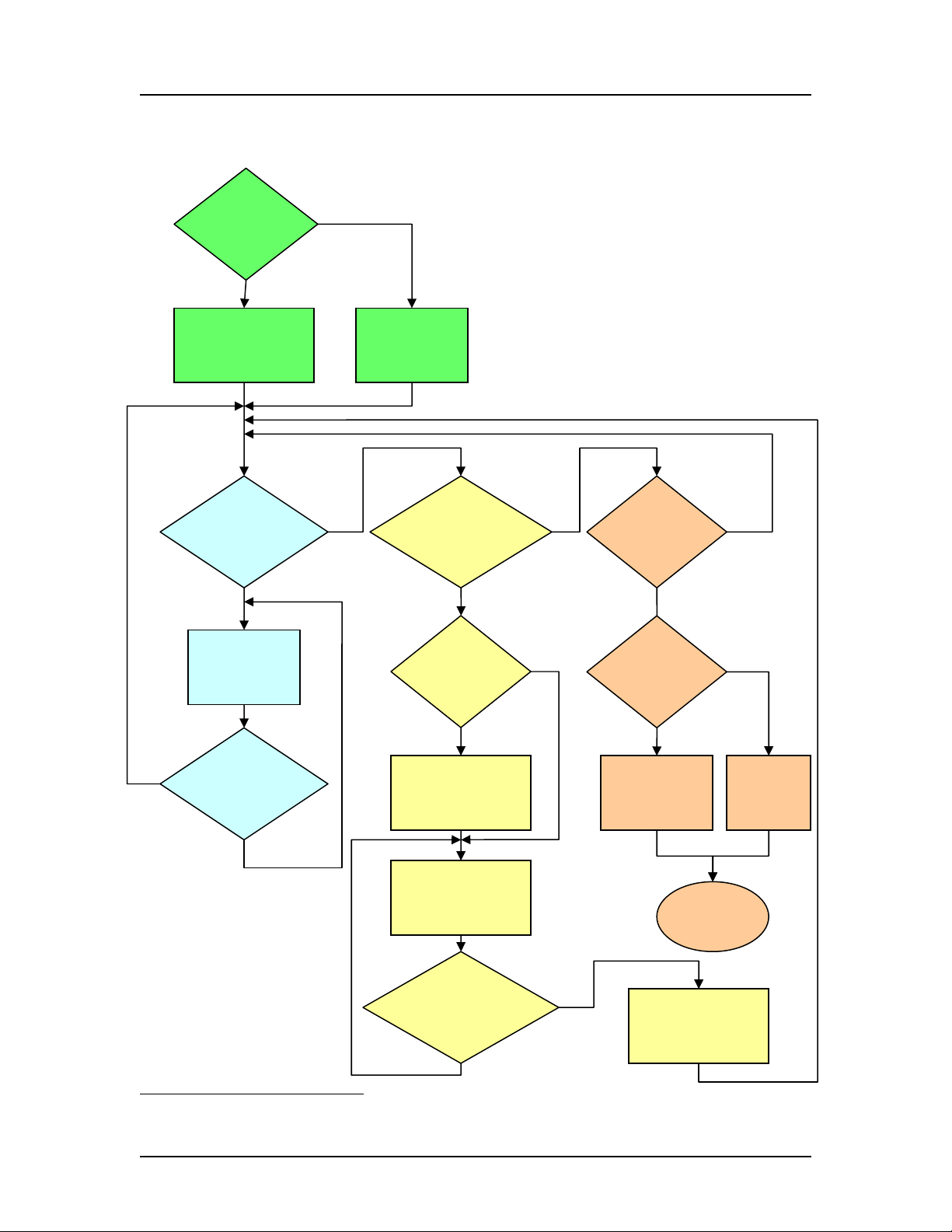
4.2 CONFIGURATION FLOW OF THE AC44906
Use AT
Commands No
?
6Any mode can be exited by resetting the transceiver; however static changes will be lost.
No
No
NoNo
NoNoNo
Send
Configuration
Command
Send CC
Command
Take Pin 17
Low
Send Exit
Configuration
Mode Command
In AT
Command
Mode?
Send AT Enter
Configuration
Mode Command
Send Enter AT
Command Mode
Command
Take Pin
17 High
Normal
Mode
Send Exit AT
Command
Mode
Send CC
Commands? Send
Configuration
Commands?
Exit
Command
Mode?
In AT
Command
Mode?
Send another
Configuration
Command?
Send another
CC
Command?
12/20/05 18

AC4490 Specifications
4.3 COMMAND QUICK REFERENCE
Below is a command reference and further information on each individual command can be found in
the text following. It is strongly recommended that all the information be read on each command prior
to using as some commands have caveats.
Command Name Command (All Bytes in Hex) Return (All Bytes in Hex)
EEPROM Byte Read C0h Starting
Address Length
(0 : 256 bytes) - C0h Starting
Address Length Data at those
addresses
EEPROM Byte Write C1h Starting
Address Length
(1 – 80h) Data bytes to
be written C1h Starting
Address Length Data written to
last byte
EEPROM Exit
Configuration Mode 56h - - - 56h - - -
AT Enter Command
Mode 41h 54h 2Bh 2Bh 2Bh 0Dh CCh 43h 4Fh 4Dh
AT Enter Configuration
Mode CCh 65h - - 65h - - -
Exit AT Command Mode CCh 41h 54h 4Fh 0Dh CCh 44h 41h 54h
Status Request CCh 00h 00h - CCh Firmware
Version
00h: Server In Range
01h: Client In Range
02h: Server Out of Range
03h: Client Out of Range
Change Channel with
Forced Acquisition CCh 02h New Channel - CCh New Channel - -
Change Server/Client
Type CCh 03h
00h: Server
03h: Client - CCh Firmware
Version 00h: Server
03h: Client
Change Sync Channel CCh 05h New Sync
Channel - CCh New Sync
Channel - -
Sleep Walk Power-Down CCh 06h - - CCh Channel - -
Sleep Walk Wake-Up CCh 07h - - CCh Channel - -
Broadcast CCh 08h
00h: Addressed
01h: Broadcast - CCh 00h or 01h - -
Write Destination
Address CCh 10h Byte 4 of
destination’s
MAC Byte 5 Byte 6 CCh Byte 4 of
destination’s
MAC Byte 5 Byte 6
Read Destination
Address CCh 11h - - CCh Byte 4 of
destination’s
MAC Byte 5 Byte 6
Auto Channel/Auto
Destination CCh 15h
Bit 0 : Auto Destination
Bit 1 : Auto Channel
Bit 4 : Enable Auto Destination
Bit 5 : Enable Auto Channel
CCh
Bit 0 : Auto Destination
Bit 1 : Auto Channel
Bits 2 – 7: 0
Read Digital Inputs CCh 20h - - CCh Bit 0 : GI0
Bit 1 : GI1 - -
12/20/05 19

AC4490 Specifications
Command Name Command (All Bytes in Hex) Return (All Bytes in Hex)
Read ADC CCh 21h 00h: AD In
01h: Temp
02h: RSSI - CCh MSB of 10 bit
ADC LSB of 10 bit
ADC -
Report Last Valid RSSI CCh 22h - - CCh RSSI - -
Write Digital Outputs CCh 23h Bit 0 : GO0
Bit 1 : GO1 - CCh Bit 0 : GO0
Bit 1 : GO1 - -
Write DAC CCh 24h Update Period Duty Cycle CCh Update Period Duty Cycle -
Set Max Power CCh 25h New Setting - CCh New Setting - -
Report Last Packet RSSI CCh 26h - - CCh RSSI - -
Transmit Buffer Empty CCh 30h - - CCh 00h - -
Disable Sync-to-Channel CCh 85h - - CCh Channel - -
Deep Sleep Mode CCh 86h - - CCh Channel - -
Read Temperature CCh A4h - - CCh Temp (°C) - -
EEPROM Byte Read CCh C0h Starting Address Length
(0 : 256
bytes) C0h Starting
Address Length Data at those
addresses
EEPROM Byte Write CCh C1h Starting
Address Length
(1 – 80h) Data bytes to
be written C1h Starting
Address Length Data written to
last byte
Soft Reset CCh FFh - - - - - -
12/20/05 20
Other manuals for AC4490
2
Table of contents
Other AeroComm Transceiver manuals

AeroComm
AeroComm AC4424 User manual

AeroComm
AeroComm CL4490-1000 User manual

AeroComm
AeroComm CL4490-1000-485 User manual

AeroComm
AeroComm PKLR2400S User manual

AeroComm
AeroComm CL4790 User manual

AeroComm
AeroComm CL4424 User manual

AeroComm
AeroComm AC4424-10 User manual

AeroComm
AeroComm AC4490 User manual

AeroComm
AeroComm AC5124 User manual

AeroComm
AeroComm AC4790 User manual


