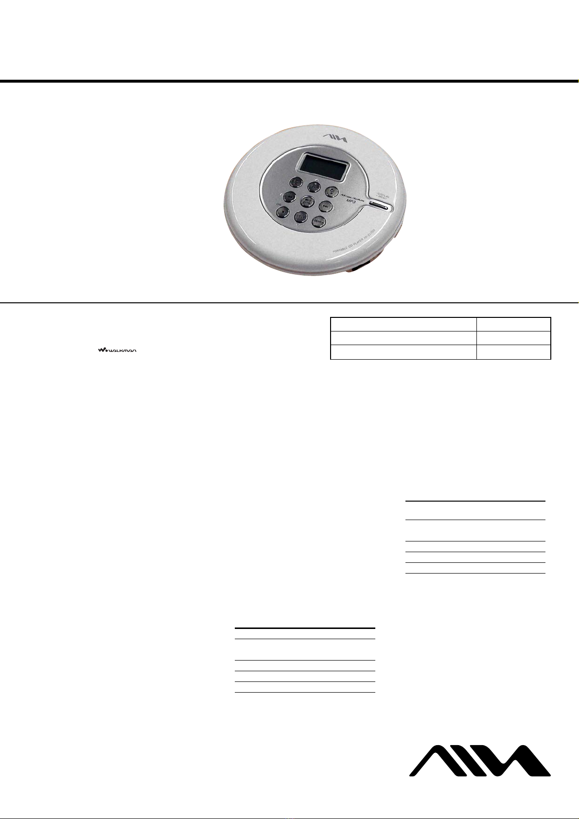
Aiwa XP-ZV700 User manual

SERVICE MANUAL
PORTABLE CD PLAYER
AEP Model
XP-ZV700/ZV701/ZV702
E Model
XP-ZV700/ZV701
Australian Model
XP-ZV700
XP-ZV700/ZV701/ZV702
Ver. 1.4 2005.10
SPECIFICATIONS
Model Name Using Similar Mechanism NEW
CD Mechanism Type CDM-3325ERV
Optical Pick-Up Name DAX-25EV
9-879-387-05
2005J05-1
© 2005.10
Sony Corporation
Personal Audio Division
Published by Sony Engineering Corporation
SonicStage and SonicStage logo are trademarks or registered trademarks of Sony Corporation.
OpenMG, Net MD, ATRAC, ATRAC3plus and their logos are trademarks of Sony Corporation.
“WALKMAN” is a registered trademark of Sony Corporation to represent Headphone Stereo
products. is a trademark of Sony Corporation.
Microsoft, Windows, Windows NT and Windows Media are trademarks or registered trademarks of
Microsoft Corporation in the United States and /or other countries.
IBM and PC/AT are registered trademarks of International Business Machines Corporation.
Macintosh is a trademark of Apple Computer, Inc. in the United States and/or other countries.
Pentium is a trademark or a registered trademark of Intel Corporation.
All other trademarks and registered trademarks are trademarks or registered trademarks of their
respective holders. ™ and ® marks are omitted in this manual.
CD and music-related data from Gracenote, Inc., copyright © 2000-2003 Gracenote. Gracenote
CDDB® Client software, copyright 2000-2003 Gracenote. This product and service may practice
one or more of the following U.S. Patents: #5,987,525; #6,061,680; #6,154,773, #6,161,132,
#6,230,192, #6,230,207, #6,240,459, #6,330,593, and other patents issued or pending.
Gracenote and CDDB are registered trademarks of Gracenote. The Gracenote logo and logotype,
the Gracenote CDDB logo, and the “Powered by Gracenote” logo are trademarks of Gracenote.
Program © 2001, 2002, 2003, 2004 Sony Corporation
Documentation © 2004 Sony Corporation
•
•
•
•
•
•
•
•
3YSTEM
#OMPACTDISCDIGITALAUDIOSYSTEM
,ASERDIODEPROPERTIES
-ATERIAL'A!L!S
7AVELENGTHLNM
%MISSIONDURATION#ONTINUOUS
,ASEROUTPUT,ESSTHAN§7
4HISOUTPUTISTHEVALUEMEASUREDATADISTANCE
OFMMFROMTHEOBJECTIVELENSSURFACEONTHE
OPTICALPICKUPBLOCKWITHMMAPERTURE
$!CONVERSION
BITQUARTZTIMEAXISCONTROL
&REQUENCYRESPONSE
(Z
n
D"MEASUREDBY*%)4!
/UTPUTAT6INPUTLEVEL
(EADPHONESSTEREOMINIJACK
!PPROXM7!PPROXM7AT7
!PPROXM7!PPROXM7AT7
&ORTHECUSTOMERSINAEP model
0OWERREQUIREMENTS
s ,2SIZE!!BATTERY6$#¾
"ATTERYLIFE
7HENUSINGONEALKALINEBATTERY
%s!s3s3'0
h%!33'0v h%!33'0v
!UDIO#$
!42!##$
-0#$
7HENUSINGONE.(7-!!RECHARGEABLE
BATTERYCHARGEDFORABOUTHOURS
%s!s3s3'0
h%!33'0v h%!33'0v
!UDIO#$
!42!##$
-0#$
-EASUREDVALUEUSINGTHE*%)4!*APAN
%LECTRONICSAND)NFORMATION4ECHNOLOGY)NDUSTRIES
!SSOCIATION
0LAYINGTIMESHOWNISAPPROXIMATEHOURSWHEN
YOUUSETHEPLAYERONAmATANDSTABLESURFACEAND
h0/7%23!6%vISSETTOh/.v.
4HISVALUEVARIESDEPENDINGONHOWTHEPLAYER
ISUSED
7HENUSINGA3ONY,23'ALKALINEBATTERY
PRODUCEDIN*APAN
– Continued on next page –
Photo: XP-ZV700
s 3ONY.(7-!!RECHARGEABLEBATTERY
6$#¾
s 3ONY.(!!"$RECHARGEABLEBATTERY
,M!H
s !#POWERADAPTOR$#).6JACK
US and foreign patents licensed from Dolby Laboratories.
%XCEPT:6: AEPMODEL&ORTHEAREACODE
OFTHEMODELYOUPURCHASEDCHECKTHEUPPERLEFT
SIDEOFTHEBARCODEONTHEPACKAGE
120 V, 60 Hz (MX model)
220 V, 50 Hz (AR model)
230 V, 50 Hz (HK model)
240 V, 50 Hz (AUS model)
100 V-240 V, 50/60 Hz (Other models)

2
XP-ZV700/ZV701/ZV702
Notes on chip component replacement
•Never reuse a disconnected chip component.
•Notice that the minus side of a tantalum capacitor may be dam-
aged by heat.
Flexible Circuit Board Repairing
•Keep the temperature of the soldering iron around 270 ˚C dur-
ing repairing.
•Do not touch the soldering iron on the same conductor of the
circuit board (within 3 times).
•Be careful not to apply force on the conductor when soldering
or unsoldering.
CAUTION
Use of controls or adjustments or performance of procedures
other than those specified herein may result in hazardous ra-
diation exposure.
SAFETY-RELATED COMPONENT WARNING!!
COMPONENTS IDENTIFIED BY MARK 0OR DOTTED LINE
WITH MARK 0ON THE SCHEMATIC DIAGRAMS AND IN
THE PARTS LIST ARE CRITICAL TO SAFE OPERATION.
REPLACE THESE COMPONENTS WITH SONY PARTS WHOSE
PART NUMBERS APPEAR AS SHOWN IN THIS MANUAL
OR IN SUPPLEMENTS PUBLISHED BY SONY.
.OTESONTHE!#POWERADAPTOR
s $ISCONNECTALLPOWERSOURCESWHENTHEPLAYERIS
NOTTOBEUSEDFORALONGTIME
s 5SEONLYTHE!#POWERADAPTORSUPPLIED)F
YOURPLAYERISNOTSUPPLIEDWITHTHEONEUSEAN
!#%('!#POWERADAPTORNOTAVAILABLEIN
!USTRALIAnAND!RGENTINA)FYOUUSEANYOTHER!#
POWERADAPTORMALFUNCTIONMAYOCCUR
0OLARITYOFTHEPLUG
s $ONOTTOUCHTHE!#POWERADAPTORWITHWET
HANDS
s #ONNECTTHE!#POWERADAPTORTOANEASILY
ACCESSIBLE!#OUTLET3HOULDYOUNOTICEAN
ABNORMALITYINTHE!#POWERADAPTORDISCONNECTIT
FROMTHE!#OUTLETIMMEDIATELY
2ECORDEDATKBPS
2ECORDEDATKBPS
#HARGINGTIMEVARIESDEPENDINGONHOWTHE
RECHARGEABLEBATTERYISUSED
%XCEPT:6: AEPMODEL
/PERATINGTEMPERATURE
##&&
$IMENSIONSWHDEXCLUDINGPROJECTINGPARTS
ANDCONTROLS
!PPROX¾¾MMb¾¾
bIN
-ASSEXCLUDINGACCESSORIES
!PPROXGOZ
$ESIGNANDSPECIlCATIONSARESUBJECTTOCHANGE
WITHOUTNOTICE
s !bbreviation
!#POWERADAPTOR
Except :6: AEPMODEL*
%ARPHONEs
:6:%,HK, AUS and ZV701: E18 models only*)
2EMOTE
:6: AEPMODEL
2ECHARGEABLEBATTERY
"ATTERYCARRYINGCASE
:6:%MODEL
:6:%MODEL
ONLY*
#$2/-3ONIC3TAGE
/PERATINGINSTRUCTIONS
)NSTALLATION/PERATING'UIDE
*&ORTHEAREACODEOFTHEMODELYOUPURCHASED
CHECKTHEUPPERLEFTSIDEOFTHEBARCODEONTHE
PACKAGE
(Other models)
%ARPHONEs
ONLY*
Clamp filter
ONLY*
:61: E18 and ZV702 models only*)
Supplied Accessories
TABLE OF CONTENTS
1. SERVICING NOTES ................................................ 3
2. GENERAL ................................................................... 5
3. DISASSEMBLY
3-1. Disassembly Flow ........................................................... 6
3-2. Cabinet (Upper) Assy, Cabinet (Lower) .......................... 6
3-3. JACK Board, Optical Pick-up Assy (CDM-3325ERV) ... 7
3-4. SWITCH Board ............................................................... 7
4. DIAGRAMS
4-1. Printed Wiring Board – EGL Board – ............................ 9
4-2. Schematic Diagram – EGL Board – ............................... 10
4-3. Printed Wiring Board
– JACK Board (Component Side) – ................................ 11
4-4. Printed Wiring Board
– JACK Board (Conductor Side) – .................................. 12
4-5. Schematic Diagram – JACK Board – ............................. 13
4-6. Printed Wiring Board – SWITCH Board – .................... 14
4-7. Schematic Diagram – SWITCH Board – ....................... 15
5. EXPLODEDVIEWS
5-1. Cabinet (Upper) Section .................................................. 23
5-2. Cabinet (Upper) Assy Section ......................................... 24
5-3. Cabinet (Lower) Section.................................................. 25
5-4. Optical Pick-up Section (CDM-3325ERV) ..................... 26
6. ELECTRICAL PARTS LIST .................................. 27
AR: Argentina model
AUS: Australian and New Zealand model
E18: Singapore model
HK: Hong Kong model
MX: Mexican model
Ver. 1.2

3
XP-ZV700/ZV701/ZV702
SECTION 1
SERVICING NOTES
NOTES ON HANDLING THE OPTICAL PICK-UP
BLOCK OR BASE UNIT
The laser diode in the optical pick-up block may suffer electrostatic
break-down because of the potential difference generated by the
charged electrostatic load, etc. on clothing and the human body.
During repair, pay attention to electrostatic break-down and also
use the procedure in the printed matter which is included in the
repair parts.
The flexible board is easily damaged and should be handled with
care.
NOTES ON LASER DIODE EMISSION CHECK
The laser beam on this model is concentrated so as to be focused on
the disc reflective surface by the objective lens in the optical pick-
up block. Therefore, when checking the laser diode emission,
observe from more than 30 cm away from the objective lens.
LASER DIODE AND FOCUS SEARCH OPERATION
CHECK
During normal operation of the equipment, emission of the laser
diode is prohibited unless the upper lid is closed while turning ON
the S502. (push switch type)
The following checking method for the laser diode is operable.
•Method:
Emission of the laser diode is visually checked.
1. Open the upper lid.
2. With a disc not set, turn on the S502 with a screwdriver having
a thin tip as shown in Fig.1.
3. Press the u ENTER button.
4. Observing the objective lens, check that the laser diode emits
light.
When the laser diode does not emit light, automatic power
control circuit or optical pick-up is faulty.
In this operation, the objective lens will move up and down 2
times along with inward motion for the focus search.
NOTES ON REPLACEMENT OF EGL BOARD OR
EEPROM (IC1602)
When EGL board is replaced or EEPROM (IC1602) on the EGL
board is replaced, patch processing is needed.
Confirm about information of patch processing to each service
headquarters.
Fig. 1 Method to push the S502
UNLEADED SOLDER
Boards requiring use of unleaded solder are printed with the lead-
free mark (LF) indicating the solder contains no lead.
(Caution: Some printed circuit boards may not come printed with
the lead free mark due to their particular size)
: LEAD FREE MARK
Unleaded solder has the following characteristics.
•Unleaded solder melts at a temperature about 40 °C higher
than ordinary solder.
Ordinary soldering irons can be used but the iron tip has to be
applied to the solder joint for a slightly longer time.
Soldering irons using a temperature regulator should be set to
about 350 °C.
Caution: The printed pattern (copper foil) may peel away if
the heated tip is applied for too long, so be careful!
•Strong viscosity
Unleaded solder is more viscou-s (sticky, less prone to flow)
than ordinary solder so use caution not to let solder bridges
occur such as on IC pins, etc.
•Usable with ordinary solder
It is best to use only unleaded solder but unleaded solder may
also be added to ordinary solder.
OPERATION CHECK WHEN THE LID IS OPEN
Inperformingthe repair withthe powersupplied to theset,removing
the JACK board causes the set to be disabled.
In such a case, make a solder bridge to short SL501 (OPEN) on the
JACK board in advance.
– JACK Board (Component Side) –
SL501
(OPEN)
S502
lever (detection)
lever (detection)
JACK board
Ver. 1.4

4
XP-ZV700/ZV701/ZV702
Providing the required system environment
The following system environment is required in order to use the SonicStage Ver. 2.3.
This software is not supported by the following environments:
•OSs other than the indicated above
•Personally constructed PCs or operating systems
•An environment that is an upgrade of the original manufacturer-installed operating system
•Multi-boot environment
•Multi-monitor environment
•Macintosh
•We do not ensure trouble-free operation on all computers that satisfy the system requirements.
•The NTFS format of Windows XP/Windows 2000 Professional can be used only with the standard
(factory) settings.
•We do not ensure trouble-free operation of the system suspend, sleep, or hibernation function on all
computers.
•For Windows 2000 Professional users, install Service Pack 3 or later before using the software.
System requirements
Computer IBM PC/AT or Compatible
•CPU:Pentium II 400 MHz or higher (Pentium III 450 MHz or higher
is recommended.)
•Harddisk drive space: 200 MB or more (1.5 GB or more is
recommended) (The amount space will vary according to Windows
version and the number of music files stored on the hard disk.)
•RAM: 64 MB or more (128 MB or more is recommended)
Others
•CDdrive(capable of digital playback by WDM)
•Sound Board
•USBport (supports USB (previously USB 1.1))
Operating
System Factory installed:
Windows XP Media Center Edition 2005/Windows XP Media Center
Edition 2004/Windows XP Media Center Edition/Windows XP
Professional/Windows XP Home Edition/Windows 2000 Professional/
Windows Millennium Edition/Windows 98 Second Edition
Display High Color (16 bit) or higher, 800 u600 dots or better (1024 u768 dots
or better is recommended)
Others •Internet access: for Web registration, EMD services and CDDB
•WindowsMedia Player (version 7.0 or higher) installed for playing
WMA files
Notes
COLOR VARIATION
Model Destination BLACK WHITE
AEP zz
E18 zz
E33 zz
XP-ZV700 MX z
HK z
AR zz
AUS zz
XP-ZV701 AEP zz
E18 z
XP-ZV702 AEP zz
•Abbreviation
AR : Argentina model
AUS:Australian and New Zealand model
E18 : Singapore model
E33 : Chilean and Peruvian model
HK : Hong Kong model
MX : Mexican model
Ver. 1.2

5
XP-ZV700/ZV701/ZV702
SECTION 2
GENERAL This section is extracted from
instruction manual.
Guide to Parts and
Controls
CD player
78 9 q;qa
12 345 6
Remote (ZV702 and ZV701: E18
models only*)
q;
3
7
2
4
qs
5
* For the area code of the model you purchased,
check the upper left side of the bar code on the
package.
1
SEARCH button
2
CD player:
ZV700: AEP model:
x
button
Other models:
x
/CHG button
Remote:
x
button
3
CD player:
u
(play/pause)*/ENTER button
Remote:
u
(play/pause)* button
4.
/
>
buttons
5
+/− buttons
6
DISPLAY/MENU button
7
CD player:
VOL +/− • f/Fbuttons
VOL +/−
f/F
Remote:
VOL +/−
8i
(headphones) jack
9
DC IN 3 V jack
q;
HOLD switch (on the back of the CD
player
qa
OPEN switch
qs
Clip
* This button has a tactile dot.
E18: Singapore model
•Abbreviation
$ISPLAY
Ȯ
#HARACTERINFORMATIONDISPLAY
ȯ
!TRACPLUS-0INDICATOR
Ȱ
$ISCINDICATOR
ȱ
"ATTERYINDICATOR
Ȳ
0LAYLISTINDICATOR
ȳ
'ROUPINDICATOR
ȴ
"OOKMARKINDICATOR
ȵ
0LAYMODEINDICATOR
ȶ
4IMERINDICATOR
ȷ
3OUNDINDICATOR

6
XP-ZV700/ZV701/ZV702 SECTION 3
DISASSEMBLY
•This set can be disassembled in the order shown below.
3-1. DISASSEMBLY FLOW
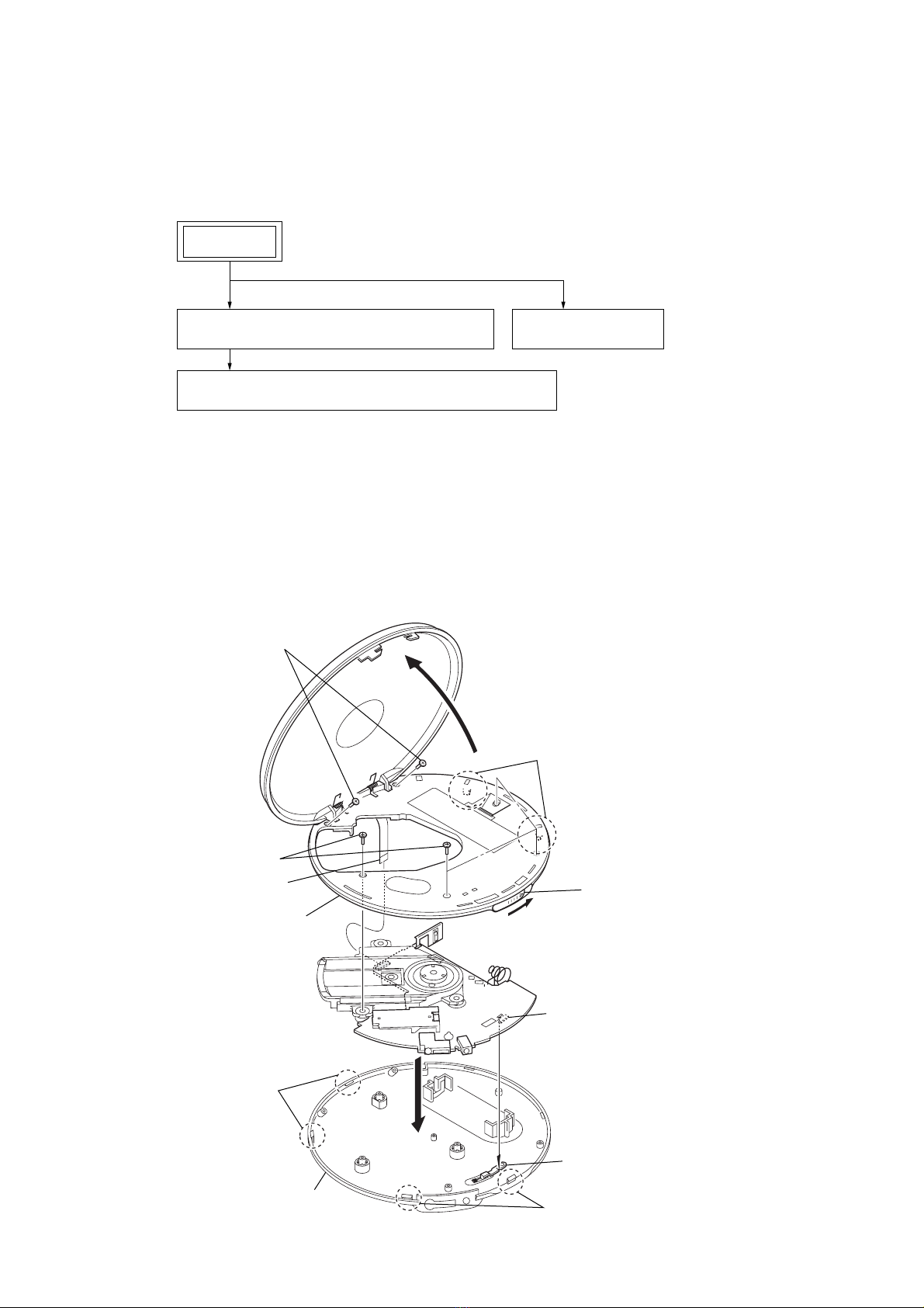
3-2. CABINET (UPPER) ASSY, CABINET (LOWER)
Note: Follow the disassembly procedure in the numerical order given.
3-2. CABINET (UPPER) ASSY , CABINET (LOWER)
(Page 6) 3-4. SWITCH BOARD
(Page 7)
3-3. JACK BOARD, OPTICAL PICK-UP ASSY (CDM-3325ERV)
(Page 7)
SET
1
Open the upper lid.
4
cabinet (lower)
5
flexible flat (12 core) cable
(CN601)
6
cabinet (upper) assy
S501
knob (hold)
Note: On installation of JACK board,
adjust the position of switch (S501)
and knob (hold).
3
two claws
3
two claws
3
two claws
2
two screws
2
four screws

7
XP-ZV700/ZV701/ZV702
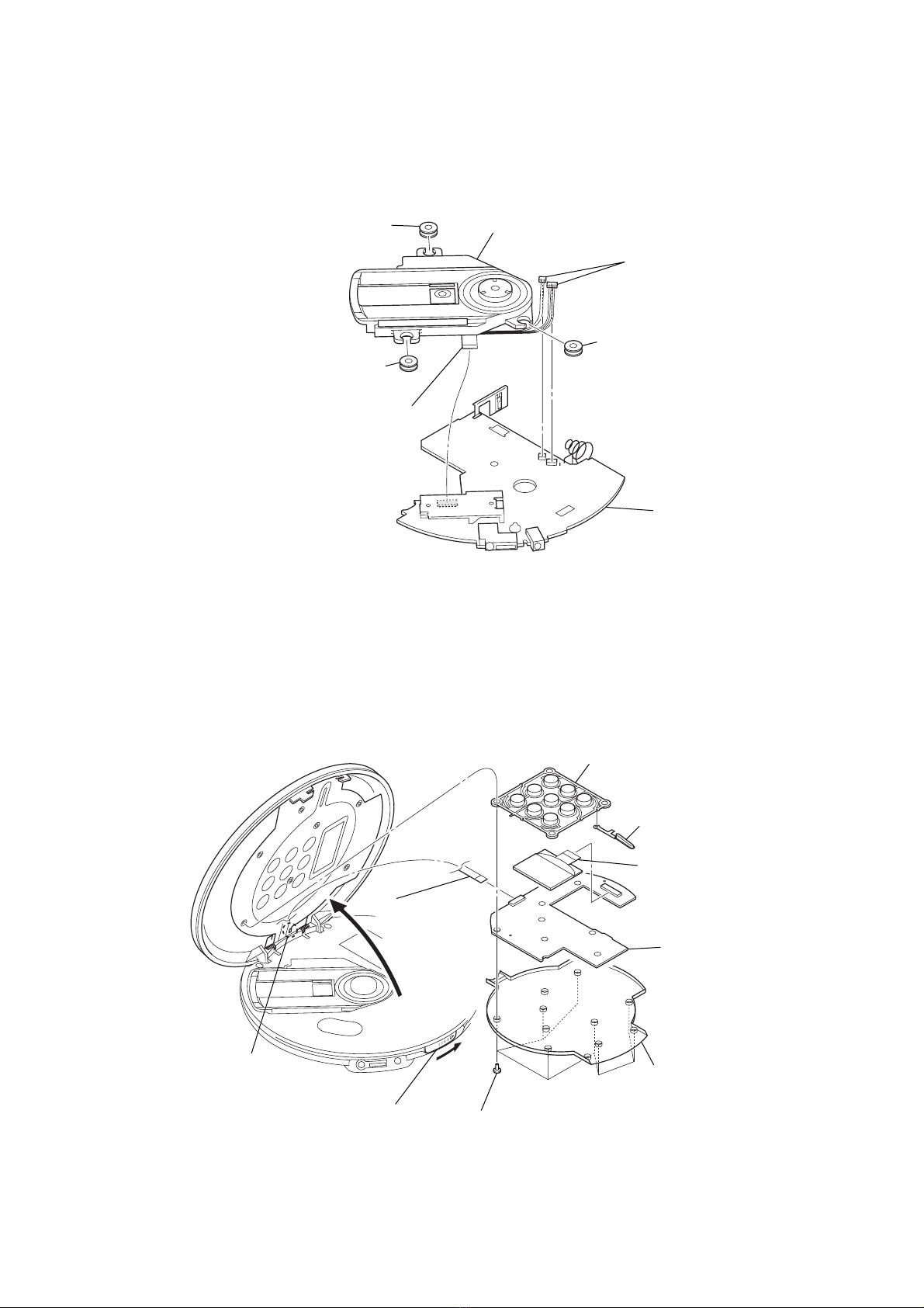
3-3. JACK BOARD, OPTICAL PICK-UP ASSY (CDM-3325ERV)
3-4. SWITCH BOARD
1
OP flexible board
(CN601)
5
optical pick-up assy
(CDM-3325ERV)
3
JACK board
4
insulator
4
insulator
4
insulator
2
two connectors
(CN401, CN402)
1
Open the upper lid.
2
eight screws
4
cover (SW PWB)
5
flexible flat
(12 core) cable
(CN1002)
3
claw
6
liquid crystal display panel
(LCD1001) (CN1001)
7
SWITCH board
9
button (operation)
8
button (menu)

8
XP-ZV700/ZV701/ZV702 SECTION 4
DIAGRAMS
Note on PrintedWiring Boards.
•X: parts extracted from the component side.
•Y: parts extracted from the conductor side.
•z: Through hole.
•f: internal component
•: Pattern from the side which enables seeing.
(The other layers' patterns are not indicated.)
•Note for PrintedWiring Boards and Schematic Diagrams
Caution:
Pattern face side: Partsonthe patternfaceside seenfrom
(Conductor Side) the pattern face are indicated.
Parts face side: Parts on the parts face side seen from
(Component Side) the parts face are indicated.
•EGL board is multi-layer printed board.
However, the patterns of intermediate-layer have not been in-
cluded in the diagram.
Note on Schematic Diagrams.
•All capacitors are in µF unless otherwise noted. (p: pF)
50 WV or less are not indicated except for electrolytics
and tantalums.
•All resistors are in Ωand 1/4W or less unless otherwise
specified.
• f: internal tolerance.
•C: panel designation.
•A: B+ Line.
•Powervoltage is dc1.5Vand fedwith regulated dc power
supply from battery terminal.
•Voltages and waveforms are dc with respect to ground
under no-signal conditions.
no mark : CD PLAY
•Voltagesaretaken with aVOM (Inputimpedance10 MΩ).
Voltage variations may be noted due to normal produc-
tion tolerances.
•Waveforms are taken with a oscilloscope.
Voltage variations may be noted due to normal produc-
tion tolerances.
•Circled numbers refer to waveforms.
•Signal path.
J: CD PLAY
•Abbreviation
AR : Argentina model
AUS:Australian and New Zealand model
E18 : Singapore model
E33 : Chilean and Peruvian model
HK : Hong Kong model
MX : Mexican model
Note: The components identified by mark 0or dotted
line with mark 0are critical for safety.
Replace only with part number specified.
Caution:
Pattern face side: Partsonthe patternfaceside seenfrom
(Side B) the pattern face are indicated.
Parts face side: Parts on the parts face side seen from
(Side A) the parts face are indicated.
•Lead Layouts
Lead layout of conventional IC CSP (chip size package)
surface
Ver. 1.3

99
XP-ZV700/ZV701/ZV702
4-1. PRINTEDWIRING BOARD – EGL BOARD – :Uses unleaded solder.
1-864-385- (12)
12
EGL BOARD
(SIDE A)
R407
R606
C680
C639
R670
C695
R621
R624
R625
C617
R614
R623
C632 C619
C631
C644
C629
C627
C662
X601
R647
C667
R631
C686
C687
R619
150
25 26
85
4
1
R406
1-864-385- (12)
12
EGL BOARD
(SIDE B)
CN9002
VDR601
R618
R632
C607
C676 C675
R602
R610
C678
C664
C646
C663
R613
R644
R653
R642
C659
C677
R604
C610
C603
R629
R638
R636 R637
R609
C608
C654
C653
C649
R628
R608
R639
C648
R634
C642 R635
C650
R656
R655
R650
R651
R649
C624 C626
C618
R669
C602 RB601
C601
R603
C694
CN601
C609
50 26
25
1
1
15
OPTICAL
PICK-UP
BLOCK
(DAX-25EV)
A
B
C
D
E
F
G
H
I
1 2 3 4 5 6 7 8 9 10
JACK BOARD
CN501
(Page 11)
A
ZV700: E18, E33, MX, HK,
AR, AUS/ZV701: E18
IC604
IC1602
IC603
Ver. 1.4
When EGL board is replaced or EEPROM (IC1602) on the EGL board is
replaced, patch processing is needed.
Confirmaboutinformation of patchprocessing to eachserviceheadquarters.

1010
XP-ZV700/ZV701/ZV702
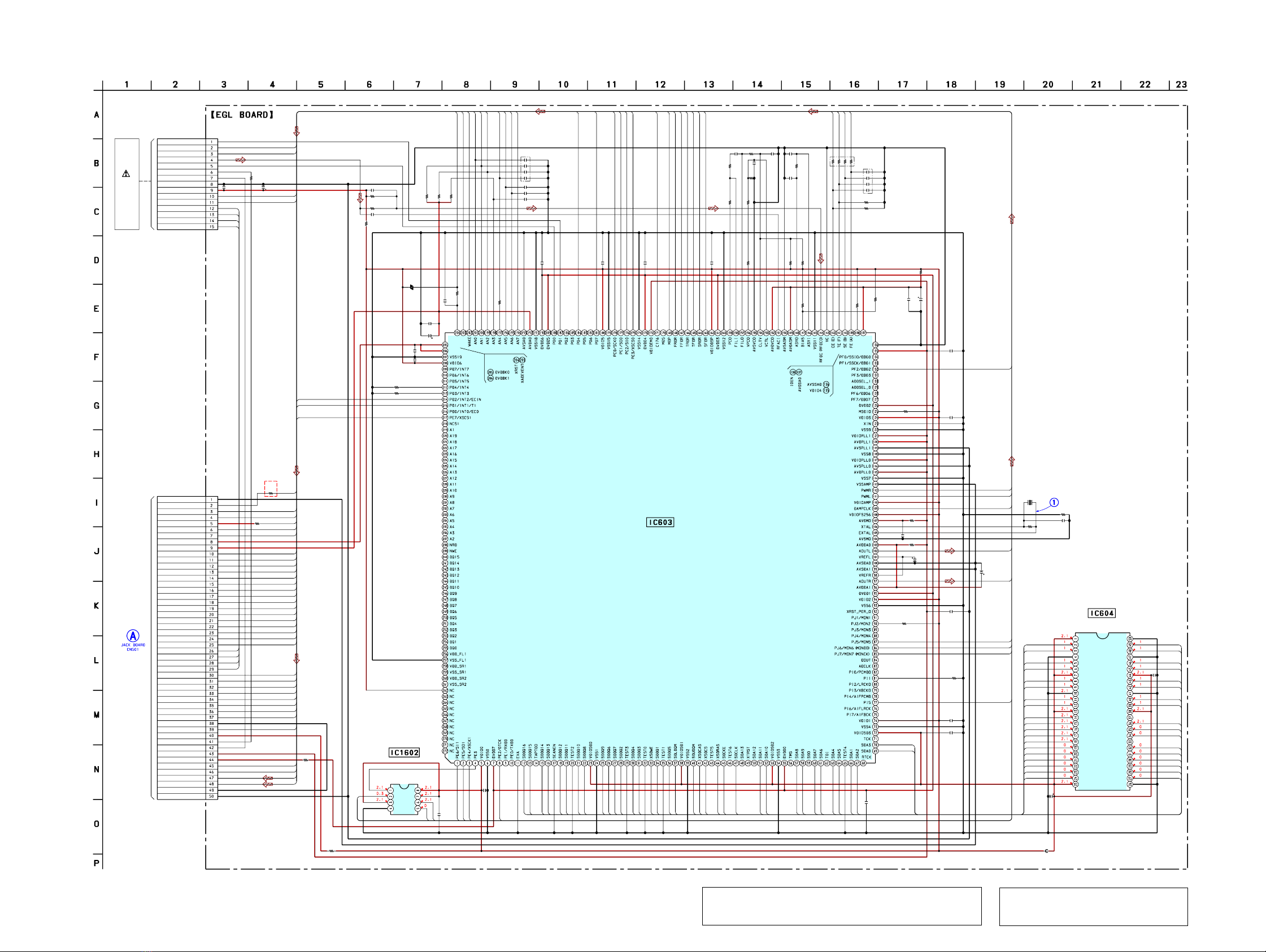
4-2. SCHEMATIC DIAGRAM – EGL BOARD –
(Page 13)
C602
C694
R602
C601
R603
R608
R609
C609
R624 R623
R618
C629
R621
C631
C632
C695
C618
C617
C619
C624
C642
R638
R629
R628
R635
R636
R634
C650 C653
R637
C654
R639
R642
R649
R604
C610
C603
R653
R613
C667
R644
X601
R606
R631
R610
C686
C687
C662
IC1602
RB601
C627
C607
C677
C664
C675
C676
C663
R406
C649
R656
R655
CN601
C608
R625
C648
R650
R651
C626 C646
C659
C680
C678
IC604
R619
C644
C639
R407
R669
R670
R614
R632
VDR601
R647
IC603
CN9002
470p
0.1
0
22 6.3V
10
47k
22k
2200p
10k 10k
1k
0.1
1k
0.1
0.1
4700p
4700p
4700p
4700p
0.1
0.1
0
2.2k
2.2k
1M
100k
10k
4700p 0.47
220k
0.1
47k
47k
22k
10
0.1
100
4V
10k
0
0.1
10
22MHz
0
220k
100k
47
6.3V
0.1
0.1
AK6510CL-L
22k
22 6.3V
0.01
0.1
47
6.3V
0.1
0.1
0.1
0
0.47
100k
47k
15P
22p
10k
0.1
100k
100k
0.1 0.1
0.1
3p
22
6.3V
MSM56X16160J-20T3
0.1
0.1
0
47k
0
0
0
10k
CXR711260-218H2
50P
FE(A)
SE(B)
TE(F)
CE(E)
SFDR
SRDR
TFDR
TRDR
FFDR
FRDR
MDP
SYNC
POWERLT
SI0
SO0
XSCK0
COLDST
LCD_XRST
OPEN
CHGMNT
BATMNT
AD_RMKEY
AD_KEY2
AD_KEY1
DCINMNT
CASINO_WAKE
XADEVENT
XRST
HOLD
PWMR
PWML
DAMPCLK
AOUTL
AOUTR
PWRSW
EN1
EN2
MUTE
SDA0
SDA1
SDA2
SDA3
SDA4
SDA5
SDA6
SDA7
SDA8
SDA9
SDA10
SDA11
SDCLK
SDCKE
SDXRAS
SDXCS
SDXCAS
SDUDQM
SDLDQM
SDDQ5
SDDQ1
SDDQ2
SDDQ3
SDDQ4
SDDQ6
SDDQ7
SDDQ8
SDDQ9
SDDQ10
SDDQ11
SDDQ12
SDDQ13
SDDQ14
SDDQ15
SDDQ16
LCD_XSCK_O
LCD_SDT_O
LCD_SDT_I
SI0
XSCK0
SO0
AOUTR
AOUTL
BEEP
PWRSW
XRST
POWERLT
SO0
SXCK0
COLDST
XADEVENT
SYNC
CASINO_WAKE
MUTE
MDP
FG
SRDR
SFDR
TRDR
TFDR
FRDR
FFDR
LCD_SDT_I
LCD_SDT_O
LCD_XSCR_O
LCD_CS
LCD_XRST
AD_KEY2
AD_KEY1
CNGMNT
HOLD
OPEN
DCINMNT
AD_RMKEY
TSB
FE(A)
SE(B)
CE(E)
TE(F)
T+
T-
F-
F+
F+
F-
T+
T-
SDDQ1
SDDQ2
SDDQ3
SDDQ4
SDDQ5
SDDQ6
SDDQ7
SDDQ8
SDLDQM
SDXWE
SDXCAS
SDXRAS
SDXCS
SDA11
SDA10
SDA0
SDA1
SDA2
SDA3
SDDQ9
SDDQ10
SDDQ11
SDDQ12
SDDQ13
SDDQ14
SDDQ15
SDDQ16
SDUDQM
SDCLK
SDCKE
SDA4
SDA5
SDA6
SDA7
SDA8
SDA9
SDXWE
TSB
BATMNT
FG
BEEP
LCD_CS
OPGSW
A
B
RF
OPSTB
LD
PD
GND_A
VCC
E
F
F+
T-
T+
F-
F-
GND_AU
AD_RMKEY
DCINMNT
VIN
OPEN
HOLD
VSTB1
VSTB2
CNGMNT
AD_KEY1
AD_KEY2
LCD_XRST
LCD_CS
LCD_CLOCK
LCD_DATA_O
LCD_DATA_I
FFDR
FRDR
TFDR
TRDR
SFDR
SRDR
FG
MDP
F+
T-
T+
MUTE
CASINO_WAKE
SYNC
WAKE
COLDST
CLOCK
LATCHB
GND
RSTB
VCC2
VAPC
PAPC
VCC0
VCC1
PWRSW
BEEP
A-L
A-R
GND
GND_A
VCC
DQ1
DQ2
VSSQ
DQ3
DQ4
VCCQ
DQ5
DQ6
VSSQ
DQ7
DQ8
VCCQ
LDQM
VSS
DQ16
DQ15
VSSQ
DQ14
DQ13
VCCQ
DQ12
DQ11
VSSQ
DQ10
DQ9
VCCQ
NC
XWE
XRAS
XCS
A11
A10
A0
A1
A2
A3
VCC
UDQM
CLK
CKE
NC
A9
A8
A7
A6
A5
A4
VSS
XCS
DO
WP
GND
VCC
HOLD
SCK
DI
XCAS
SD-RAM
EEPROM
OPTICAL
PICK-UP
BLOCK
(DAX-25EV)
SYSTEM CONTROLLER,
DSP,LCD DRIVER
CSP
(Chip Size Package)
DATA
SP_DTC/STB
ZV700:E18,E33,MX, HK,
AR,AUS/ZV701:E18
(
(
• See page 16 forWaveforms. • See page 16 for IC Pin Function Description.
The components identified by mark 0or dotted
line with mark 0are critical for safety.
Replace only with part number specified.
Ver. 1.4
When EGL board is replaced or EEPROM (IC1602) on the EGL board is
replaced, patch processing is needed.
Confirmaboutinformation of patchprocessingto each serviceheadquarters.

1111
XP-ZV700/ZV701/ZV702
4-3. PRINTEDWIRING BOARD – JACK BOARD (COMPONENT SIDE) – :Uses unleaded solder.
• Semiconductor
Location
Ref. No.
Location
D302 F-7
D401 A-7
D402 E-7
D404 C-6
D405 C-7
D407 C-7
D411 C-6
IC301 H-4
IC501 D-8
Q401 B-7
Q402 E-7
Q401 B-7
Q402 E-7
Q404 A-6
Q408 D-6
Q410 D-7
D402
Q402
D302
D401
Q404
R410
C410
C401
C414
R451
R438 L413
C418
L417
C421
R416
C442
C419
Q401
D405
D404
D407
R430
R429
C422
C441
L411
L412
C438
L414
L416
L415
R457
D411
C431
C443
C428
R442
R441
R443
R440
C429
Q408
Q410
R427
C403
C432
C409 FB404
C405
FB401
R439
R502
R504
C501
C502
VDR401
FB402
C407
R305
C311
FB303
L201
R203
L501
C202
C102
C301
L301
C304
R301
C308
C305
CN501
CN402 CN401
C423
C402
R407
C302
C208
C108
13 12
1
24
SL501
(OPEN)
JACK BOARD
(COMPONENT SIDE)
1-864-027- (11)
11
-1
-2
8
14
5
25
1
50
26
U
V
W
M401
(SPINDLE)
1
4
14
M402
(SLED)
M
A
EGL BOARD
CN9002
(Page 9)
1
3
4
6
12
S502
OPEN
A
B
C
D
E
F
G
H
1 2 3 4 5 6 7 8
(ZV701: E18/ZV702)
(ZV700/ZV701: AEP)
IC301
IC501
Ver. 1.1

1212
XP-ZV700/ZV701/ZV702
4-4. PRINTEDWIRING BOARD – JACK BOARD (CONDUCTOR SIDE) – :Uses unleaded solder.
• Semiconductor
Location
Ref. No.
Location
D101 F-3
D201 G-3
D301 E-3
D303 E-2
D304 E-2
D403 B-3
D406 C-2
D408 D-2
D412 B-2
IC401 C-3
Q403 B-2
Q409 D-4
DRY BATTERY
SIZE “AA”
(IEC DESIGNATION LR6)
1PC 1.5V
RECHARGEABLE
BATTERY
NH-7WMAA 1PC 1.2V 700 mAh
(NH-AA-B2D 1PC 1.2V 2300 mAh)
(EXCEPT ZV700: AEP)
(ZV701: E18/ZV702)
FB304
R456
D403
R418
R409
D412
Q403
R420
C420
C417
R432
R428
R455
C439
R419
C425
R416
C435
C434
R433
R403
C436
C411
R415
R507
R423
D406
C426
R417
R413
C444
D408
C433
C412
C413
R431
Q409
R426
R425
R424
R421
C503
C437
R404 R405
C504
FB502
R402
R411
C404
TH401
D303
D304
VDR309
D301
C107
R104
D101
D201
L101
C207
R204
R103
C204
R201
R101
R102
C104
C103
R111
C203
R211
C307
C303
R202
FB605
FB604
FB603
FB602
FB601
FB608 FB607
FB606
C601
C602
CN601
F401
C406
R412
40
41
21
20
1
80
60
61
FB306
JACK BOARD (CONDUCTOR SIDE)
1-864-027- (11)
11
FB609
1
12
S501
HOLD
HOLD
r
OFF
DC IN 3V
–+
J402
J301
A
B
C
D
E
F
G
H
1 2 3 4 5 6 7 8
B
SWITCH
BOARD
CN1002
(Page 14)
9
EXCEPT
ZV700:AEP
(ZV701: E18/ZV702)
(ZV701: E18/ZV702)
(ZV701: E18/ZV702)
IC401
Ver. 1.1

1313
XP-ZV700/ZV701/ZV702
4-5. SCHEMATIC DIAGRAM – JACK BOARD –
(Page 10)
(Page 15)
R413
C426
C411
C412
C413
R412
C435 C434
C417
C420
CN601
R423 C416
C414
C425
R438
R428
R455
R431
C418
R433
R457
C442
C419
D405
R430
R429
C421
C422
R403
R440R439
C436
R417
C428C429
C431
C432
C443
R424 R425
R416
R456
IC301
C308
R301
R102
R101
C104C103
R111
C203
R211
C204
C302R103
R204
C207
R426
D402
R504
C501
R502
R402 C437
R419
R411
C404R404
C402
C403
D401
C407
C433
R415
Q409
R410
C503
C504
FB601
FB602
FB603
FB604
FB605
C601
C602
FB606
FB607
CN401
CN402
M401
M402
D406
L413
Q401
L414
D404
C441
C410
D407
R432
L412 L411
L416
D411
L415
C444
R441
R421
C423
IC501
R507
C502
S502 SL501
S501
R202
R201
L301
FB303
L201
1 mH
1 mH
L101
VDR309
FB402 VDR401
C405
C401
C108
C208
R203
D304
TH401
C406
C305
R104
D301
D302
C107
FB306
D101
D201
D408
L501
FB502
J402
F401
C409 R405
D403
CN501
R407
Q403
R418 R409
R451
L417
C439
C304
C307
C303
FB404
FB401
R420
FB608
D412
J301
Q402
Q408
Q404
FB609
C102
C202
C301
IC401
Q410
D303
FB304
R305
C311
R442
R443
C438
47k
0.22
0.01
0.01
0.01
4.7k
1000p 220p
0.47
1
12P
100 100p
0.47
0.01
100k
2.2k
0
0
47
4V
22k
0
0.01
100 6.3V
RB521S-30FTE61
220
220
100
4V
0.01
2.2M
1k4.7
0.1
0
47
6.3V
47
6.3V
2.2
47
6.3V
2.2
220k 220k
100
100k
TA2152FN(EL)
4.7
100
22k
47k
2.22200p
2.2k
2200p
2.2k
2.2
0.1470
1
0.22
470k
MA2YD2300LS0
1M
470p
0
10k 0.22
220
47k
0.22220k
220
4V
4.7
MA22D2800LS0
1
4.7
47k
2SA1832FV
(H3SONY)
0
1000p
1000p
1
1
4P
2P
MA22D2800LS0
NTHD4508N
RB521S
-30FTE61
1
22
4V
RB521S-30FTE61
1k
MA785-(TX),SO
1000p
10k
10k
100
4V
RT8H055C
0
4700p
22k
47k
0
1
1
0.22
0.22
470
MA8051-TX
0.1
10
16V
1
MA8051-TX
MA8051-TX
0.22
RSB6.8STE61
RSB6.8STE61
RB521S-30FTE61
1.4A
32V
10 47k
UDZSTE-174.7B
50P
100
2SD2652
0.47 0.47
100k
1
10 10V
2.2
0.1
220
UDZSTE-175.6E
2SA1363-T111-1E
UMT1N-TN
DTC115TE
0
220
4V
220
4V
100
4V
SC901591AFR2
2SC4154TP-IF
MA8051-TX 0
0.0047
47k
22k
0.22
PAPC
VAPC
MDP
FG
AD_RMKEY
RS
COM
U
V
W
F+
F-
T-
T+
S-
S+
RS
CHGSW
DATA_O
DATA_I
AD_KEY1
AD_KEY2
COM
W
V
U
S+
S-
SRDR
SFDR
CHGMNT
TFDR
TRDR
FFDR
FRDR
DATA
CLOCK
COLDST
WAKE
SYNC
RSTB
BEEP
MUTE
PWRSW
LCH
RCH
AD_RMKEY
HOLD
OPEN
CASINO_WAKE
AD_RMKEY
DCINMNT
OPEN
HOLD
CHGMNT
AD_KEY1
AD_KEY2
XRST_I
LCD_CS_I
CLK_I
DATA_O
DATA_I
FFDR
FRDR
TFDR
TRDR
SFDR
SRDR
FG
MDP
F+
F-
T-
T+
MUTE
CASINO_WAKE
SYNC
WAKE
COLDST
CLOCK
DATA
LATCHB
RSTB
VAPC
PAPC
PWRSW
BEEP
LCH
RCH
DCINMNT
CHGSW
LATCHB
CLK_I
LCD_CS_I
XRST_I
IF
NC
VIN
VCC
GND
OUT
RF
INM
PAPC
VAPC
GND
VREF
VIN
SW
VCP
VCC2
VSTB2
VSTB1
VCC1
APWM
PWM
FG
RMCRB
CPUI
CPVI
CPWI
COM
VMVW
GNDW
VMU
GNDUV
FO3
VM3
RO3
RO2
VM2
FO2
HBGND12
HBGND23
RO1
VM1
FO1
HBGND1
TEST
RSTB
SYNC
WAKE
COLDST
CLOCK
LATCHB
EXTRSTB
DCIN
CRF
CINM
BATM
CHGSW
RSOSCR
OSCC
R13
F13
R12
F12
INPVD
INP0
VD
VDLX
VD_T
VD_B
VCC0
L0_1
L0_2
PGND1
PGND2
C1L
C1H
CINP
VG
CHGMON
FI1
RI1
W
VU
COM
CLK_I
LCD_CS_I
DATA_O
DATA_I
XRST_I
VCC0_+2.7V
AD_KEY1
AD_KEY2
PS
SGND
COM
W
V
U
S+
S-
GND_AU
SP_DTC/TSB
AD_RMKEY
DCINMNT
VIN
OPEN
HOLD
VSTB1
VSTB2
CHGMNT
AD_KEY1
AD_KEY2
LCD_XRST
LCD_CS
LCD_CLOCK
LCD_DATA_O
LCD_DATA_I
FFDR
FRDR
TFDR
TRDR
SFDR
SRDR
FG
MDP
F+
F-
MUTE
CASINO_WAKE
SYNC
WAKE
COLDST
CLOCK
DATA
LATCHB
GND
RSTB
VCC2
VAPC
PAPC
VCC0
VCC1
PWRSW
BEEP
A-L
A-R
GND
T-
T+
NC
NC
BEEPO_L
OUT_L
EQ_L
OUT_C
PGND
EQ_R
OUT_R
BEEPO_R
VCC2
IN_R
OUT_ADJ
BIAS_I
RF_IN
C-AMP_SW
GND
BIAS_O
BEEP_I
PW_SW
MU_TC
VCC1
IN_L
VCC2_+2.1V
D_GND
(SPINDLE)
(SLED)
S
S
DATA
FOCUS/TRACKING COIL DRIVE,
SPINDLE/SLED MOTOR DRIVE
POWER CONTROL
SWITCING
-1-2
Q408,410
DC DETECT
VOLTAGE DETECT
(OPEN)
OPEN
HOLD
HOLD
OFF
MUTE_SW
GND_A
HEADPHONE AMP
DRY BATTERY
SIZE"AA"
(IEC DESIGNATION LR6)
DC IN 3V
RIPPLE FILTER
CHARGE
SWITCH
1PC 1.5V
B+ SWITCH
NH-7WMAA
(EXCEPT ZV700:AEP)
(ZV701:E18/ZV702)
(EXCEPT ZV700:AEP)
(ZV701:E18/ZV702)
(EXCEPT ZV700:AEP)
1PC 1.2V 2300mAh
CPV0
VO0
WO
VO
UO
B+ SWITCH
(
ZV700/
ZV701:AEP
RECHARGEBLE BATTERY
NH-AA-B2D
1PC 1.2V 700mAh
(
(ZV701:E18/ZV702)
47mH
10mH
10mH
100mH
10mH
47mH
22mH
47mH 47mH
(
(
(
• See page 16 forWaveforms. • See page 16 for IC Block Diagram. • See page 16 for IC Pin Function Description.
The components identified by mark 0or dotted
line with mark 0are critical for safety.
Replace only with part number specified.
Ver. 1.1

1414
XP-ZV700/ZV701/ZV702
4-6. PRINTEDWIRING BOARD – SWITCH BOARD – :Uses unleaded solder.
R1113
S1007
C1001
VDR1001
R1104
R1108
R1107
R1110
R1111
R1112
S1011
S1010
S1005
S1004
S1008
S1003
S1001
R1005
R1004
R1003
R1002
R1001
CN1002
R1135
R1102
R1103
R1101
R1105
R1109
R1114
R1106
S1009
C1008
CN1001
C1007
C1006
C1003
C1004
C1005
C1010
C1011
C1012
C1002
S1002
SWITCH BOARD
1-864-579-
123
LCD1001
LIQUID CRYSTAL DISPLAY
B
JACK
BOARD
CN601
(Page 12)
1
12
–
v
VOL+ +
VOL–
V
u
ENTER
DISPLAY
MENU
>B
SEARCH
b.
x
CHG
x
(ZV700:AEP)
EXCEPT
ZV700:AEP
A
B
C
D
E
F
G
1 2 3 4 5 6 7 8
(11)
11

1515
XP-ZV700/ZV701/ZV702
4-7. SCHEMATIC DIAGRAM – SWITCH BOARD –
(Page 13)
C1007
R1001
R1002
R1003
R1004
R1005
R1101
R1102 R1103
R1104
R1105
R1107
R1108 R1110
R1111
R1112
CN1002CN1001
VDR1001
R1109
R1113
R1114 R1106
C1002
C1001
S1005
S1004S1003
S1002S1001
S1011
S1010 S1009
S1008
S1007
R1135
C1012
C1003
C1011
C1004
C1010
C1005
C1006
C1008
0.22
1k
1k
1k
1k
1k
10k
4.7k 2.2k
22k
2.2k
10k
22k 2.2k
2.2k
22k
12P23P
1k
47k
4.7k 4.7k
0.1
0.1
0
0.22
0.22
0.22
0.22
0.22
0.22
0.22
0.47
SCK
CSB
SDI
SDO
RSTB
VDD
VSS
VREF
VCIN
CP1
CN1
CP2
CN2
CP3
CN3
VSSL
VCOUT
VLCIN
V1
V2
V3
V4
V5
CLK_I
LCD_CS_I
DATA_O
DATA_I
LCD_XRST
D_GND
AD_KEY1
AD_KEY2
PS
SGND
SEARCH
-
ENTER
VOL -
+
VOL +
DISPLAY
MENU
LCD1001
LIQUID
CRYSTAL
DISPLAY
VCC2_+2.1V
VCC0_+2.7V
CHG
EXCEPT
ZV700:AEP
(ZV700:AEP)
(
(

1616
XP-ZV700/ZV701/ZV702
•IC Block Diagram
– JACK Board –
• IC Pin Function Description
IC301 TA2152FN (EL)
+
–
24
OUT ADJ
23
BIAS IN
22
RF IN
21
C-AMP SW
20
GND
19
BIAS OUT
18
BEEP IN
17
MUTE SW
16
PW SW
15
MUTE TC
14
VCC1
13
INB
1
NC
2
NC
3
BEEP OUTB
4
OUTB
5
EQB
6
OUTC
7
PW GND
8
EQA
9
OUTA
10
BEEP OUTA
11
VCC2
12
INA
+
–
BIAS
C-AMP SW BEEP PW/MUTE SW
PWA PWC PWB
1X601
500 mV/DIV, 20 ns/DIV
45.5 ns 1.1 Vp-p
qa IC401 wd (SYNC)
(CD play mode)
1 V/DIV, 1
µ
s/DIV
2.8
µ
s2.1 Vp-p
2.8
µ
s2.7 Vp-p
qs IC401 ta (LO_2), ts (LO_1)
1 V/DIV, 1
µ
s/DIV
•Waverforms
– EGL Board – – JACK Board –
EGL BOARD IC603 CXR711260-218H2 (SYSTEM CONTROLLER, DSP, LCD DRIVER)
Pin No. Pin Name I/O Description
1
PE6/SI1 I Serial data input from the liquid crystal display
2
PE5/SO1 O Serial data output to the liquid crystal display
3
PE4/XSCK1 O Serial clock signal output to the liquid crystal display
4
PE3 O Chip select signal output to the EEPROM
5
VDIO0 - Power supply terminal (+2.1V)
6
VSS0 - Ground terminal
7
DVDD7 - Power supply terminal (+1.3V)
8
PE2/DTCK I/O Not used
9
PE1/RXD0 I Not used
10
PE0/TXD0 O Not used
11
EVA - Not used
12, 13
SDDQ16, SDDQ15 I/O Two-way data bus with the SD-RAM
14
TAPTDO - Not used
15, 16
SDDQ14, SDDQ13 I/O Two-way data bus with the SD-RAM
17
SCANEN - Not used
18, 19
SDDQ12, SDDQ11 I/O Two-way data bus with the SD-RAM
20
TEST2 - Not used
21, 22
SDDQ10, SDDQ8 I/O Two-way data bus with the SD-RAM
23
VDIOSD0 - Power supply terminal (+2.7V)
24
VSS1 - Ground terminal
25 to 28
SDDQ9, SDDQ6,
SDDQ7, SDDQ2 I/O Two-way data bus with the SD-RAM
29
TEST3 - Not used
30, 31
SDDQ4, SDDQ3 I/O Two-way data bus with the SD-RAM
32
TEST0 - Not used
33
XSDWE O Write enable signal output to the SD-RAM
34
SDDQ1 I/O Two-way data bus with the SD-RAM
35
TEST1 - Not used
36
SDDQ5 I/O Two-way data bus with the SD-RAM
37
SDLDQM O Lower byte input/output mask signal output to the SD-RAM
38
VDIOSD1 - Power supply terminal (+2.7V)
39
VSS2 - Ground terminal
40
SDUDQM O Upper byte input/output mask signal output to the SD-RAM
41
XSDCAS O Column address strobe signal output to the SD-RAM
42
XSDCS O Chip select signal output to the SD-RAM
43
TEST5 - Not used
44
XSDRAS O Row address strobe signal output to the SD-RAM
45
SDCKE O Clock enable signal output to the SD-RAM
46
TEST6 - Not used
47
SDCLK O Clock signal output to the SD-RAM
48
SDA13 O Address signal output to the SD-RAM
49
XTRST - Not used
50 to 52
SDA12 to SDA10 O Address signal output to the SD-RAM
53
VDIOSD2 - Power supply terminal (+2.7V)
54
VSS3 - Ground terminal
55
DVDD0 - Power supply terminal (+1.3V)
Ver. 1.4

17
XP-ZV700/ZV701/ZV702
Pin No. Pin Name I/O Description
56 TMS - Not used
57, 58 SDA8, SDA9 O Address signal output to the SD-RAM
59 TDO - Not used
60, 61 SDA7, SDA6 O Address signal output to the SD-RAM
62 TDI - Not used
63, 64 SDA5, SDA4 O Address signal output to the SD-RAM
65 TEST4 - Not used
66, 67 SDA1, SDA2 O Address signal output to the SD-RAM
68 RTCK - Not used
69, 70 SDA0, SDA3 O Address signal output to the SD-RAM
71 TCK - Not used
72 VDIOSD3 - Power supply terminal (+2.7V)
73 VSS4 - Ground terminal
74 VDIO1 - Power supply terminal (+2.1V)
75 PI7/AIFBCK - Not used
76 PI6/AIFLRCK - Not used
77 PI5 O Muting on/off control signal output to the headphone amplifier "H": muting on
78 PI4/AIFPCMD - Not used
79 PI3/XBCKO - Not used
80 PI2/LRCKO - Not used
81 PI1 - Not used
82 PI0/PCMDO - Not used
83 ADCLK - Not used
84 DOUT - Not used
85 PJ7/MON7
(MONCK) - Not used
86 PJ6/MON6
(MONDO) - Not used
87 PJ5/MON5 O Amplifier power on/off control signal output to the headphone amplifier
"H": amplifier power on
88 to 91 PJ4/MON4 to
PJ1/MON1 - Not used
92 XRST_PWR_O - Not used
93 VSS6 - Ground terminal
94 VDIO2 - Power supply terminal (+2.1V)
95 DVDD1 - Power supply terminal (+1.3V)
96 AVDDA1 - Power supply terminal (+2.7V)
97 AOUTR O Analog audio signal output to the headphone amplifier (R-ch)
98 VREFR O Reference voltage output terminal (R-ch)
99, 100 AVSDA1, AVSDA0 - Ground terminal
101 VREFL O Reference voltage output terminal (L-ch)
102 AOUTL O Analog audio signal output to the headphone amplifier (L-ch)
103 AVDDA0 - Power supply terminal (+2.7V)
104 AVSMO - Ground terminal
105 EXTAL O System clock output terminal (22 MHz)
106 XTAL I System clock input terminal (22 MHz)
107 AVDMO - Power supply terminal (+2.7V)
108 VDIOFS256 - Power supply terminal (+2.1V)

18
XP-ZV700/ZV701/ZV702
Pin No. Pin Name I/O Description
109 DAMPCLK - Not used
110 VDIOAMP - Power supply terminal (+2.1V)
111 PWML - Not used
112 PWMR - Not used
113 VSSAMP - Ground terminal
114 VSS7 - Ground terminal
115 AVDPLL0 - Power supply terminal (+2.7V)
116 AVSPLL0 - Ground terminal
117 VDIOPLL0 - Power supply terminal (+2V)
118 VSS8 - Ground terminal
119 AVSPLL1 - Ground terminal
120 AVDPLL1 - Power supply terminal (+2.7V)
121 VDIOPLL1 - Power supply terminal (+2V)
122 VSS9 - Ground terminal
123 XIN - Not used
124 VDIO3 - Power supply terminal (+2.1V)
125 MSDIO - Not used
126 DVDD2 - Power supply terminal (+1.3V)
127, 128 PF7/DBG7,
PF6/DBG6 - Not used
129, 130 ADDSEL_0,
ADDSEL_1 - Not used
131 PF3/DBG3 - Not used
132 PF2/DBG2 I HOLD switch input terminal "L": hold on
133 PF1/SSCK/DBG1 - Not used
134 PF0/SSIO/DBG0 - Not used
135 VDIO4 - Power supply terminal (+2V)
136 AVSSAD - Ground terminal
137 AVDSAD - Power supply terminal (+2.1V)
138 IGEN I Stabilized current input for operational amplifiers
139 FE (A) I A signal input from the optical pick-up block
140 SE (B) I B signal input from the optical pick-up block
141 TE (F) I F signal input from the optical pick-up block
142 CE (E) I E signal input from the optical pick-up block
143 VC I Middle point voltage input terminal Not used
144 RFDC (RFDCO) I RF signal input from the optical pick-up block
145 VSS11 - Ground terminal
146 ASYI I Asymmetry comparator voltage input terminal
147 BIAS I Asymmetry circuit constant current input terminal
148 ASYO O EFM full-swing output terminal
149 AVDASM - Power supply terminal (+2.1V)
150 AVSASM - Ground terminal
151 RFACI I EFM signal input from the optical pick-up
152 AVDVCO - Power supply terminal (+2.1V)
153 VCTL I VCO control voltage input terminal for the wideband EFM PLL
154 CLTV I Internal VCO control voltage input terminal
155 AVSVCO - Ground terminal
156 VPCO O Charge pump output terminal for the wideband EFM PLL

19
XP-ZV700/ZV701/ZV702
Pin No. Pin Name I/O Description
157 FILO O Filter output terminal for master PLL
158 FILI I Filter input terminal for master PLL
159 PCO O Charge pump output terminal for master PLL
160 VSS12 - Ground terminal
161 DVDD3 - Power supply terminal (+1.3V)
162 VDIODSP - Power supply terminal (+2V)
163 SFDR O Sled servo drive signal (+) output to the motor/coil drive
164 SRDR O Sled servo drive signal (-) output to the motor/coil drive
165 TFDR O Tracking servo drive signal (+) output to the motor/coil drive
166 TRDR O Tracking servo drive signal (-) output to the motor/coil drive
167 FFDR O Focus servo drive signal (+) output to the motor/coil drive
168 FRDR O Focus servo drive signal (-) output to the motor/coil drive
169 MDP O Spindle motor servo drive signal output to the motor/coil drive
170 MDS - Not used
171 C176 O 176.4 kHz clock signal output to the motor/coil drive
172 VDIOEM0 - Power supply terminal (+2V)
173 DVDD4 - Power supply terminal (+1.3V)
174 VSS14 - Ground terminal
175 PC3/XSCS0 O Command latch signal output to the power control
176 PC2/SI0 I Serial data input from the EEPROM
177 PC1/SO0 O Serial data output to the power control and EEPROM
178 PC0/SCK0 O Serial clock signal output to the power control and EEPROM
179 VSS15 - Ground terminal
180 VDIO5 - Power supply terminal (+2V)
181 PG7 I Cold start flag input from the power control
182, 183 PG6, PG5 - Not used
184 PG4 O Reset signal output to the liquid crystal display
185, 186 PG3, PG2 - Not used
187 PG1 O Standby signal output to the optical pick-up block
188 PG0 O RF gain-up signal output for CD-RW to the optical pick-up block
189, 190 DVDD5, DVDD6 - Power supply terminal (+1.3V)
191 VSS18 - Ground terminal
192 AVDAD - Power supply terminal (+2V)
193 AVSAD - Ground terminal
194 AN7 I CD lid open/close switch input terminal "L": close, "H": open
195 AN6 I Charge voltage monitor input from the power control
196 AN5 I Battery voltage monitor input terminal
197 AN4 I Wake up signal input from the power control
Remote commander key input terminal (ZV701: Singapore/ZV702 models only)
198 AN3 - Not used
199, 200 AN2, AN1 I Top panel key input terminal (A/D input)
201 AN0 I DCIN voltage monitor input terminal
202 WAKE I Wake up signal input terminal
203 XADEVENT O Wake up signal output to the power control
204 XRST I System reset signal input from the power control
205, 206 DVDBK0, DVDBK1 - Power supply terminal (+1.2V)
207 VSS19 - Ground terminal
208 VDIO6 - Power supply terminal (+2V)

20
XP-ZV700/ZV701/ZV702
Pin No. Pin Name I/O Description
209 to 213 PD7/INT7 to
PD3/INT3 - Not used
214 PD2/INT2/ECIN I FG signal input from the motor/coil drive
215 PD1/INT1/T1 O Beep signal output to the headphone amplifier
216 PD0/INT0/EC0 - Not used
217 PE7/XSCS1 O Command latch signal output to the liquid crystal display
218 NCS1 - Not used
219 to 237 A0, A19 to A1 - Not used
238 NRD - Not used
239 NWE - Not used
240 to 255 DQ15 to DQ0 - Not used
256 VDD_FL1 - Power supply terminal Not used
257 VSS_FL1 - Ground terminal
258 VDD_SR1 - Power supply terminal Not used
259 VSS_SR1 - Ground terminal
260 VDD_SR2 - Power supply terminal Not used
261 VSS_SR2 - Ground terminal
262 to 272 NC - Not used
This manual suits for next models
2
Table of contents
Other Aiwa CD Player manuals