TABLE
OF
CONTENTS
SPECIFICATIONS
Six
ciuiesnudhe
tocea
avai
icen
ant
alenhec
na
Satan
ans
nats
aie
toead
ati
teiuat
anita
etaaiantetetiontoated
3
SPECIFICATIONS
<HE,
HR,
LH,
EZ,
K>...........
a
eaieneles
as
Sanitation
Moeeatbeta
ae
Reena
acne,
4
NT
cde
ge ag
fh:
SG
|
a
-
fo
0
On
eo
a
ee
5
PROTECTION
OF
EYES
FROM
LASER
BEAM
DURING
SERVICING.......ccccscscssscsessessssssessecsesnssneseseseeneenss
6
HATO
y
7
3B
OER
/
PRECAUTION
TO
REPLACE
OPTICAL
BLOCK.........cccccccscssesssetseeteeseeeeeees
6
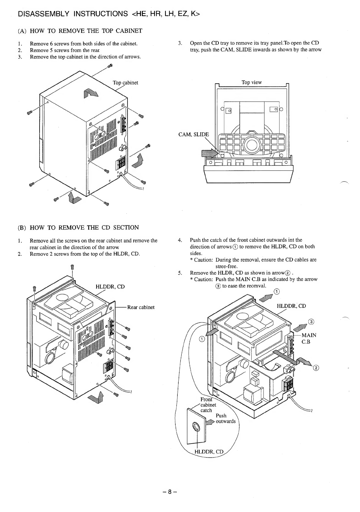
DISASSEMBLY
INSTRUCTIONS
<i
i5sacts
criescisesaecteesss
austd
sega
sunce
an
cahestavelgdi
std
Aniedendel
ban
at
ee
leat
7
DISASSEMBLY
INSTRUCTIONS
<HE,
HR,
LH,
EZ,
K>.....scccccsssscsssssssssssssssssesseessssssscseescaneesssessessesneseensarsaeensavess
8
ELECTRICAL
MAIN
PARTS
LIST
....c.cccscssssssscsessscecsescscssssccsssssensssscncssccncsessscsssssssssssenesessueaeenssassessseneesessened
9~13
CHIP
RESISTOR:
PART
CODE
v.3histeismaveengenn
ulead
duh
Grane
eaat
ate
enheesin
uuaaats
13
TRANSISTOR
ILLUSTAATION
sain
slonaceiea
sasuke
Gas
ssa
date
vasvers
vss
earsea
owes
ah
ans
mn
Gace
ane
waitin
14
IG
BLOCK:
DIAGRAM
2
1
soe.
ccssiteasts
scene
tencaleSentyahiaeiicamieeiaGa
edie
ee
eae
mamta
15
~17
BLOCK
DIAGRAM
—1
(MAIN
/
FRONT
/
PT
/
DECK
/
RELAY)
....cssecsessessessessesssssseessecsessssassussecssencarssceneans
15
~16
BLOCK
DIAGRAM
—2
(CD/CD
LOAD
/
CD
DRIVE)
.....ccccssessssesesessssesseesesseenessesnesessessssusseessanesesseesessssessseess
17
SCHEMATIC
DIAGRAM
—
1
(MAIN
(1
/
2)
/
RELAY)
.....ccccccscssessecessecsscsesscsnssecsesessussssecnscussesanensaneseeneesees
18
~
20
IG-BEOGK
“DIAGRAM
=
2
iv
as
scestecrassaidacteiarive
ssnntt
vies
biel
Moiceoaeeanon
em
aslame
anda
temeansachands
21
~
22
SCHEMATIC
DIAGRAM
—2
(MAIN
(2/2):
TUNER
SECTION)
<D,
HE,
HR,
LH>
......ceccccssesseseeseeeeseneees
23
~
24
WIRING
—
1
(MAIN)
<D,
HE,
HR,
LH>........cccscsssssssssssecssseesessessssssssssssescsecsesssssesassncesesscsesasescesssessessesecseensens
25
~
26
SCHEMATIC
DIAGRAM
—3
(MAIN
(2/2):
TUNER
SECTION)
<EZ,
K>
o.cccecccsscssesessessesessestesseseeeesseseees
27
~
28
NAVIN
2
SMAI)
Sl
ec
ache
ENR
lea
A
MN
a
Sarda
a
ca
aedlarecabin
29
~
30
SCHEMATIC
DIAGRAM
—4
(FRONT
/
DECK)
.....c.secessessessessesseesessecnesussnesessecsecseenssnssnesesseeacsueseeaeenssneaeeseees
31
~
32
WIRING
=3
(BRONT
FDE
CK
RELAY
ici
santsnestcsdivatocsancac
eatin
salsavssbetud
abies
nat
sceieiaivieciesttacherede
ete
33
~
34
SCHEMATIC
DIAGRAM—5
(CD/
CD
LOAD
/
CD
DRIVE)
....scsscsesessssesseessesessesnessesteseessersaneseeseesseeneeees
35
~
36
WIRING
=4
(CD:/'
CD
LOAD
/1CD~
DRIVED
sitssasscazestraciascuctatdeaderstiaaagedieneasaeletlodaardctudvetionbansdalandenidsaonecandls
37
~
38
SCHEMATIC
DIAGRAM
6:
(PT
)icesivatsieasesons
sa
cst
ecestcvist
sad
vcpasulaoee
year
cavauch
aye
ie
stoemacssastssneluatedue
ths
advlcsenaehacaeeed
39
WAV
HERING
3
Te)
sesucees
cacieecsnicrass
outs
aac
tas
tcc
reset
sev
ante
cctea
i
reawsason
tuts
ed
etna
peace
eee
tuatlatae
yi
pee
tte
40
FL
(SVA-11MM23)
GRID
ASSIGNMENT
/
ANODE
CONNECTION/
PIN
CONNECTION
....scecsccsssssseesesessseen
41
IS
DESCRIP
WON
SDs
rsasheissriensivtestetanitanin
tan
isan
ohintaneeainagutint
asa
meen
amen
nen
mannan
eT
AS
IG
DESCRIPTION
SIGS
FIR
Lh,
2
eS
isso
ca
cia
ct
ha
nach
Seaeebtadaesuinasbrasbeclonhsbeswendaals
cadens
tighe
ecg
dieasanaediceed
49
~
55
ADJUSTMENT
a8)
TUNER
ADS
cue
c
ia
Sacer
a
es
a
caren
et
een
da
56
ADJUSTMENT
=2
<TUNER®
HE,
AR}
Ey
EZ.
besides
cccncects
visits
tcasntk
acvadur
eater
seals
ito
tavbetaanaudinasenneies
57
~
58
PD
IS
TE
NM
ee
S20
ccs
sic
cea
sens
crectent
hea
Senaanyeu
tevad
eng
Ste
Gael
te
dane
nad
aah
iPatinn
Ui
hagas
59
PRACTICAL
“SERVICE
FIGURE
scvizicncusinnniiasersscaiadsasraicions
bodes
iiaahertvaleilbuattdadadanpianiyn!
Laihascspet
ante
daleeh
tl
60
MECHANICAL
‘EXPLODED:
VIEW
4.1.4
ssicssesousodsctenscsastsscssentedagacsunsnsdssérstisctovdebenesttuasandiedbisvesceaiuavstnieienmess
61
~
62
MECHANICAL”
PARTS
LIST
-(Acccse.cccch
sacs’
caxssacea
peated
otc
anke
luneced
dat
etsve
sanradeebanlelvagesigsaategeaevide
healt
63
~
64
TAPE
MECHANISM
EXPLODED
VIEW
1/1
....ccccssssssscsssssssssesssssessecsecsscssssssesssssasssssserssasaneesesssassncasescseeesd
65
~
66
TAPE
MECHANISM
PARTS
LIST
1/1
.....ccscsssccssssesesssesesssssessessessessessssscsscsncsssseesesscenceussesssenssucseaneausanessevcseeneeed
67
SPRING:
APPLICATION
sPOSITION
Secsxan
che
ciaccctessesat
ncaecscieshiz-ieanedba
did
a
ubaeeneaNehdianleliaaneldncseaeus
easniniad
68
CD
MECHANISM
EXPLODED
VIEW
1/2
.....ccccsssssssssscsessesssssecscstsssssssssssessecesesstscsscsecsestessnssssacasssesuessenesauentocans
69
CB.
MECHANIGM
PARES)
IST
S124
utara
rl
i
aea
a
ecistenncntlatnc
ein
ch
adem
natn
caine
70
CD
MECHANISM
EXPLODED
VIEW
2/2
....cccsccssssssssessssssssscsesssssessssosssssosssssscsesesessssssacsesssensamssssassunsssassncasesseos
71
CD
MECHANISM:
PARTS
LIST
2)
2
i
stcssczscpanpteiiacsesactnie
suersamudavtbay
vacudsbacjad
ana
eatactitebiivtia
radiata
atan
tierdentein
71
ACCESSORIES
/
PACKAGE
LIST.
j
easiaus
passerine
egies
WiSesaisabawhabilelOied
anal
auanisivanh
bss
vnethaa
temas
wlentucra:
atonal
2
PREPPING
“NAIVE
(EIST
ceviciarsanapecsceectuspitedesdeuisaitacd
sniul
OaBeatieintapeencrteddiabaniqin
ball
Mateisianiaviueucntatien
he
—